EP1030470B1 - Systèmes de communication optiques utilisant des amplificateurs optiques à semi-conducteur - Google Patents
Systèmes de communication optiques utilisant des amplificateurs optiques à semi-conducteur Download PDFInfo
- Publication number
- EP1030470B1 EP1030470B1 EP00301028A EP00301028A EP1030470B1 EP 1030470 B1 EP1030470 B1 EP 1030470B1 EP 00301028 A EP00301028 A EP 00301028A EP 00301028 A EP00301028 A EP 00301028A EP 1030470 B1 EP1030470 B1 EP 1030470B1
- Authority
- EP
- European Patent Office
- Prior art keywords
- optical
- bit
- channels
- power
- channel
- Prior art date
- Legal status (The legal status is an assumption and is not a legal conclusion. Google has not performed a legal analysis and makes no representation as to the accuracy of the status listed.)
- Expired - Lifetime
Links
- 230000003287 optical effect Effects 0.000 title claims description 91
- 239000004065 semiconductor Substances 0.000 title claims description 43
- 238000004891 communication Methods 0.000 title claims description 27
- 238000001514 detection method Methods 0.000 claims description 29
- 230000000694 effects Effects 0.000 claims description 22
- 238000000034 method Methods 0.000 claims description 17
- 238000009499 grossing Methods 0.000 claims description 4
- 239000000835 fiber Substances 0.000 description 27
- 238000009826 distribution Methods 0.000 description 19
- 230000005540 biological transmission Effects 0.000 description 16
- 238000005259 measurement Methods 0.000 description 6
- 238000010586 diagram Methods 0.000 description 5
- 239000006185 dispersion Substances 0.000 description 5
- 238000005516 engineering process Methods 0.000 description 5
- 229920006395 saturated elastomer Polymers 0.000 description 5
- 239000013307 optical fiber Substances 0.000 description 4
- 230000007704 transition Effects 0.000 description 4
- 238000013459 approach Methods 0.000 description 3
- 229910052691 Erbium Inorganic materials 0.000 description 2
- 230000003321 amplification Effects 0.000 description 2
- 230000008901 benefit Effects 0.000 description 2
- 230000000593 degrading effect Effects 0.000 description 2
- UYAHIZSMUZPPFV-UHFFFAOYSA-N erbium Chemical compound [Er] UYAHIZSMUZPPFV-UHFFFAOYSA-N 0.000 description 2
- 238000002474 experimental method Methods 0.000 description 2
- 230000006855 networking Effects 0.000 description 2
- 230000009022 nonlinear effect Effects 0.000 description 2
- 238000003199 nucleic acid amplification method Methods 0.000 description 2
- 238000005086 pumping Methods 0.000 description 2
- 229910003327 LiNbO3 Inorganic materials 0.000 description 1
- 230000003044 adaptive effect Effects 0.000 description 1
- 230000008859 change Effects 0.000 description 1
- 230000000295 complement effect Effects 0.000 description 1
- 239000002131 composite material Substances 0.000 description 1
- 230000008878 coupling Effects 0.000 description 1
- 238000010168 coupling process Methods 0.000 description 1
- 238000005859 coupling reaction Methods 0.000 description 1
- 238000005388 cross polarization Methods 0.000 description 1
- 230000001419 dependent effect Effects 0.000 description 1
- 238000013461 design Methods 0.000 description 1
- 230000009931 harmful effect Effects 0.000 description 1
- 239000000463 material Substances 0.000 description 1
- 230000010287 polarization Effects 0.000 description 1
- 230000008569 process Effects 0.000 description 1
- 238000011084 recovery Methods 0.000 description 1
- 238000012552 review Methods 0.000 description 1
Images




Classifications
-
- H—ELECTRICITY
- H04—ELECTRIC COMMUNICATION TECHNIQUE
- H04B—TRANSMISSION
- H04B10/00—Transmission systems employing electromagnetic waves other than radio-waves, e.g. infrared, visible or ultraviolet light, or employing corpuscular radiation, e.g. quantum communication
- H04B10/29—Repeaters
- H04B10/291—Repeaters in which processing or amplification is carried out without conversion of the main signal from optical form
- H04B10/293—Signal power control
- H04B10/294—Signal power control in a multiwavelength system, e.g. gain equalisation
- H04B10/296—Transient power control, e.g. due to channel add/drop or rapid fluctuations in the input power
-
- H—ELECTRICITY
- H04—ELECTRIC COMMUNICATION TECHNIQUE
- H04B—TRANSMISSION
- H04B10/00—Transmission systems employing electromagnetic waves other than radio-waves, e.g. infrared, visible or ultraviolet light, or employing corpuscular radiation, e.g. quantum communication
- H04B10/29—Repeaters
- H04B10/291—Repeaters in which processing or amplification is carried out without conversion of the main signal from optical form
- H04B10/2912—Repeaters in which processing or amplification is carried out without conversion of the main signal from optical form characterised by the medium used for amplification or processing
- H04B10/2914—Repeaters in which processing or amplification is carried out without conversion of the main signal from optical form characterised by the medium used for amplification or processing using lumped semiconductor optical amplifiers [SOA]
Definitions
- the invention relates generally to semiconductor optical amplifiers and, more particularly, to lightwave systems and networks utilizing such amplifiers.
- Optical amplifiers are commonly used in lightwave communication systems as in-line amplifiers for boosting signal levels to compensate for losses in a transmission path, as power amplifiers for increasing transmitter power, and as pre-amplifiers for boosting signal levels before receivers.
- WDM wavelength division multiplexed
- Erbium-doped fiber amplifiers are predominantly used in current WDM communication systems because of their gain characteristics and ease of coupling with optical fiber. Erbium-doped fiber amplifiers are particularly desirable for intensity modulated digital optical communication systems, wherein the light intensity of signal channels is modulated to represent the "1"s and "0"s of digital data. In particular, slow gain dynamics allow erbium-doped fiber amplifiers to provide constant gain to all signal channels in a WDM system regardless of bit transitions in the intensity modulated bit patterns.
- erbium-doped fiber amplifiers are well known
- erbium-doped fiber amplifiers are expensive and, as a result, do not provide the most cost effective solution for applications such as metropolitan optical networking and the like.
- erbium-doped fiber amplifiers have a relatively narrow usable gain bandwidth which will become more of a problem in emerging long haul systems which have higher channel counts and which will use new optical fiber having a wider usable bandwidth.
- semiconductor optical amplifiers are comparatively inexpensive, have a large gain bandwidth, and can be easily integrated with other devices.
- semiconductor optical amplifiers have several limitations which have limited their use in optical communication systems to date.
- the fast gain dynamics and nonlinear gain characteristics of semiconductor optical amplifiers can be problematic. For example, gain changes quickly as input power changes and is not constant for the modulation speed of current communication systems, thus resulting in problems such as inter-modal distortion and saturation induced crosstalk, i.e., cross-saturation.
- cross-saturation results when intensity modulation in one channel leads to modulation of the gain available for other channels.
- the gain of a specific channel is saturated not only by its own power, but also by the power of the other channels in the system.
- Cross-saturation is particularly problematic in intensity modulated systems because the channel power changes with time depending on the bit pattern.
- the signal gain of one channel then changes from bit to bit, and the change depends on the bit patterns of the other channels.
- Such gain fluctuations can result in detection errors which degrade overall bit error rate performance.
- Cross-saturation can be avoided by operating in the small signal region, i.e., unsaturated region.
- this solution is not practical for WDM systems which traditionally operate in the saturation region because of pumping efficiencies and other system considerations, e.g., high saturated power needed for wide dynamic range and high signal to noise ratios.
- Substantially error-free communications is achieved in an optical communication system comprising optical amplifiers according to the principles of the invention by detecting bits transmitted in the amplified optical signal according to a detection threshold that is derived as a function of a maximum power level associated with a first bit value, e.g., bit "0", and a minimum power level associated with a second bit value, e.g., bit "1".
- this detection scheme can be used to accurately detect the bit patterns in the amplified signal even in the presence of nonlinear distortions such as inter-modal distortion and saturation induced crosstalk.
- accurate detection of individual bits in each of the channels is possible even with the nonlinear distribution of power in each of the channels resulting from gain variations caused by the nonlinear distortions.
- the detection threshold is set at a level corresponding to P TOTAL /2N, where P TOTAL represents the total power in the WDM signal and N represents the number of optical channels in the WDM signal.
- the effect of gain variations becomes smaller as the number of optical channels within the wavelength division multiplexed signal increases.
- a smoothing effect is realized for the total effective saturation power as gain variations decrease as a function of an increase in the number of channels.
- the performance of a semiconductor optical amplifier according to the principles of the invention approaches the linear performance of fiber amplifiers as the number of channels increases.
- a system operated according to the principles of the invention therefore includes all the benefits of semiconductor optical amplifiers, e.g., lower cost and large gain bandwidth, while avoiding the problems associated with nonlinear performance of semiconductor optical amplifiers and without requiring significant device changes as suggested by the prior art. Consequently, such a solution can be readily implemented and advantageously used, especially in metropolitan area optical networking applications where cost is a primary consideration.
- WDM wavelength division multiplexed system
- the principles of the invention may also be employed in conjunction with other types of optical communication systems and other types of optical amplifiers.
- the principles of the invention can be applied to single channel optical communication systems and also to systems comprising other types of optical amplifiers having gain dynamics that rise to the aforementioned problems.
- the illustrative embodiments of the invention are described with reference to digital communications in which data is transmitted using bits "0" and "1", it will be appreciated that the inventive aspects are also applicable to other coding and modulation schemes. Accordingly, the embodiments shown and described herein are only meant to be illustrative and not limiting.
- optical amplifiers used for in-line amplification in WDM systems typically operate in the saturation region due to pumping efficiency and system considerations. In the saturation region, the output power of the amplifier is substantially fixed for a certain range of input power variations. As a result, the gain of the amplifier does not remain constant with the changes in input power.
- the output power of the amplifier must also be sufficiently high so that the signal to noise ratio at the receiver is high enough to permit accurate detection of the bit patterns transmitted in the intensity modulated signal.
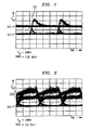
- FIG. 1 is an eye diagram of a signal channel wherein the output power, Pour, exhibits inter-modal distortion. More specifically, power level 101 represents a steady state power level for a "0" bit and power level 102 represents a steady state power level of a "1" bit in the channel.
- transition point 103 When a transition from a "0" to "1" occurs in the transmitted bit pattern, represented here as transition point 103, the power level of the "1" bit actually exceeds the steady state value 102 for a certain period of time, thus resulting in gain fluctuations in the amplified signal. Consequently, this type of nonlinear distortion, which is dependent on the intensity modulation within the signal channel, can cause problems in the detection of bits, thus degrading the overall bit error rate performance of the system.
- FIG. 2 is an eye diagram for one of the signal channels in a 2-channel system.
- the output power Pour in a signal channel depends on the state of the other channels through cross-saturation, which is the so-called crosstalk effect in WDM systems.
- the output power P OUT in one signal channel is affected by intensity modulation in the other channel in the system and will vary at random since each channel is independently modulated.
- power level 201 represents a power level for a "0" bit
- power level 202 represents a range of power levels for a "1" bit in the channel.
- the power level of a "1" bit in the channel will vary according to the power level in the other channel of the system.
- slow gain dynamics of the erbium-doped fiber amplifiers provide an advantage for modulation speeds of interest because the amplifier does not "respond" to the transitions in bits of "1"s and "0"s in the optical channels. Consequently, the erbium-doped fiber amplifier only sees the average power and therefore provides constant gain to the signal channels. As such, the gain of an erbium-doped fiber amplifier exhibits a linear characteristic such that inter-modal distortion and cross-saturation are not significant problems.
- the gain dynamics of a semiconductor optical amplifier are much faster than that of an erbium-doped fiber amplifier.
- the gain of a semiconductor optical amplifier changes rapidly as the input power changes and, as a result, the gain is not constant for the modulation speed of current communication systems.
- the gain of a semiconductor optical amplifier exhibits a nonlinear characteristic which causes the aforementioned problems of inter-modal distortion and cross-saturation which, in turn, can cause errors in the detection of bits transmitted within the channels of an optical communication system. Consequently, we have identified a need to solve the aforementioned problems so that semiconductor optical amplifiers can become a suitable alternative for single channel and WDM systems instead of the more expensive and bandwidth-limited erbium-doped fiber amplifiers.
- the detection threshold level corresponds to the total output power of the amplified WDM signal divided by two times the number of optical channels in the amplified WDM signal.
- FIG. 3 shows how thresholds are typically assigned for erbium-doped fiber amplifier systems, which will provide a better understanding of how detection thresholds are selected for semiconductor optical amplifiers according to the principles of the invention shown in FIG. 4
- P TOTAL The total output power is represented as P TOTAL .
- FIGS. 3 and 4 show the distribution of output power as viewed from the perspective of only one of the channels in the system. Using FIG 4 as an example, the distribution of output power P OUT for one of the 2 channels is shown in segment 301, the output power P OUT for one of the 4 channels is shown in segment 302, and so on.
- the linear performance causes each channel to take an equal share of the total output power, represented as P TOTAL /N Consequently, the threshold for detection can then be set at the average power of P TOTAL /N, with some variation that may be dictated by other practical considerations. Given the linear gain characteristics of erbium doped fiber amplifiers, there will only be one possible value for the "1" bit.
- the amplifier output power of any one of the channels will fluctuate with some probability distribution according to the modulation of the other channels because of the aforementioned cross saturation effects.
- N channels there will be N possible values for bit "1" in any given channel.
- bit "1" there will be two possible values for a bit "1" for a 2-channel system, four possible values for 4-channel system, and so on.
- a bit "0" in the channel will have an output power level corresponding to level 305, while a bit "1" in the channel could have one of two values.
- the maximum possible output power value for a bit "1" in a channel will be P TOTAL when all the other channels have a bit "0" simultaneously.
- the minimum possible output power value for a bit “1” will always be P TOTAL / N , when all the channels have a bit "1” simultaneously.
- the other intermediate output power values of a bit "1”, e.g., output power level 315, will assume values within a probability distribution when there is a combination of "0"s and "1"s in the other channels. This case is clearly shown for the 4-channel power distribution (302) as well as the other exemplary power distributions in FIG. 4.
- the detection threshold 310 (P TH ) would therefore be set at 1/4 th of the total output power P TOTAL .
- the detection threshold level P TH may be adjusted to be approximately greater than or less than P TOTAL /2 N , depending on other system considerations.
- the effect of gain fluctuations becomes smaller as the number of channels increases thereby resulting in a smoothed total effective power effect.
- the bit patterns in the channels of a WDM signal are pseudo-random and are independent of each other, the total power is smoother in a WDM system with multiple channels.
- This smoothed power effect can be seen in FIG. 4 where the distribution peak of output power levels for a bit "1" becomes more narrow and concentrated as the number of channels increases. For example, the distribution peak 325 for a 16-channel system is narrower than that of the systems having a lower number of channels.
- This smoothed total effective power reduces input power variation and, as a result, reduces the associated gain ripples.
- the performance of a semiconductor optical amplifier will approach the linear performance of an erbium-doped fiber amplifier.
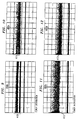
- FIGS. 5-8 show the distribution of power in only one of the channels to illustrate the cross-saturation effect from the other channels.
- FIGS 5-8 illustrate how regions 400-403, which represent the output power distribution of a bit "1", become more defined (e.g., the distribution width of bit "1" reduces) while the eye opening becomes larger as the number of channels increases from 2 to 32 channels.
- the bit "1" has two possible values.
- the bit "1" has four possible values, which are also blurred by noise.
- the channel number is increased to 8 and 32 as shown in FIGS. 7 and 8, the bit "1" becomes more clearly defined and the eye opening becomes larger.
- FIGS 9-12 further illustrate the more defined and narrower distribution peaks 410-413 of the bit "1" output power distribution as the number of channels increases from 2 to 16 channels.
- noise from the transmitter and receiver in a system may also contribute to the width of bit "1” and degrade bit-error-rate (BER) performance.
- BER bit-error-rate
- the linewidth of bit "1" can also be significantly increased due to nonlinear effects in transmission fiber.
- semiconductor optical amplifiers used in accordance with the principles of the invention will therefore be able to provide smoother total effective saturation power with smaller gain variations.
- the power smoothing effect can be effectively used not only to design and control optical communication systems and networks, but the principles also apply to digital systems operating with more than two levels.
- the smoothed total effective power can also improve the performance of analog communication systems.
- the power in bit "1" is assumed to be a constant for all signal channels.
- the power in bit "1" is likely to become non-uniform after the first amplifier.
- the dispersion in the transmission fiber can cause relative shifts in the bits of different signal channels.
- transmission fiber does have finite dispersion, the bits in different channels travel at different speeds which causes the bits to shift relative to each other during transmission.
- the equivalent input power at a subsequent semiconductor optical amplifier in the cascaded chain may be higher or lower than the nominal input power. Consequently, the total input power to subsequent semiconductor optical amplifiers in the cascaded chain can fluctuate and cause further distortion.
- inventive aspects described herein may be applied to address this problem, for example, by setting a lower detection threshold P TH i.e., a prescribed level below P TOTAL /2N, to ensure accurate detection. Additionally, well known dispersion compensating techniques may also be used in conjunction with the invention to lessen the effects of dispersion in a fiber.
- the semiconductor optical amplifier operates under strong saturation conditions. If the amplifier is operated under less saturation or even in the linear region, the distortion and crosstalk will be less. Accordingly, the detection threshold level P TH can also be adjusted as needed in these cases
- the noise figure for semiconductor optical amplifiers e.g. typically 6 dB or higher
- the output power e.g., typically 15 dBm or lower
- other techniques may be used for addressing some of the other nonlinear effects of fiber-based systems, such as four-wave-mixing, self-phase-modulation, and cross-phase-modulation, to name a few.
- the principles of the invention address the saturation induced crosstalk effects which have prevented widespread use of semiconductor optical amplifiers in WDM applications. With these problems solved, the principles of the invention can therefore be readily applied to provide a low cost solution for WDM transmission, such as in metropolitan applications and the like.
- FIG. 13 An exemplary wavelength division multiplexed system 600, which can be used in conjunction with the principles of the invention, is shown in FIG. 13.
- system 600 included a transmitter portion 601, a transmission section 625, and a receiver portion 650.
- Polarization selector 615, cross-polarization monitor 616, erbium doped fiber amplifier 617, and optical attenuator 618 were also used in transmitter portion 601 according to well-known techniques and principles of operation.
- Transmission section 625 included two semiconductor optical amplifiers 626-627, each of which was coupled at its output to a 55 km segment of Lucent Technologies' TrueWave optical fiber 628. Single stage semiconductor optical amplifiers without gain control were used for the experiment. For amplifiers 626-627, the input power was maintained at -5 dBm, the gain was 13 dB, and the output power was 8 dBm. Both amplifiers were strongly saturated The pump current was 200 mA for both amplifiers 626-627 .
- band-pass-filter 651 was used to select one channel at a time for appropriate measurement, e.g., BER and eye measurement.
- detector 652 was used to detect bits in the 32 channels using an optimum detection threshold level according to the principles of the invention.
- Other components in receiver portion 650 were used in accordance with well known principles of operation.
- erbium-doped fiber amplifier 660 was used to provide appropriate pre-amplification.
- Optical attenuator 661 and eye monitor 662 were used to facilitate the measurement of the incoming signal patterns.
- Attenuator 663, power meter 664, clock recovery circuit 665, and bit error rate tester 666 were used to facilitate the measurement of power and bit error rate in the received signals.
Landscapes
- Physics & Mathematics (AREA)
- Electromagnetism (AREA)
- Engineering & Computer Science (AREA)
- Computer Networks & Wireless Communication (AREA)
- Signal Processing (AREA)
- Optical Communication System (AREA)
- Semiconductor Lasers (AREA)
- Lasers (AREA)
Claims (10)
- Procédé de détection de bits dans un système de communications optiques (600) comprenant au moins un amplificateur optique à semi-conducteur (626), ou autre type d'amplificateur optique ayant une dynamique de gain essentiellement identique à celle des amplificateurs optiques à semi-conducteur, pour amplifier un signal optique, le signal optique ayant une pluralité de canaux optiques ou longueurs d'onde respectives aptes à être modulés afin de transmettre des informations sous forme de bits, le procédé étant CARACTERISE PAR l'étape de :en présence de distorsion causée par des variations de gain, détection de bits transmis dans le signal amplifié au moyen d'un niveau de seuil de détection (310) qui est approximativement égal à la puissance de sortie totale du signal amplifié divisée par deux fois le nombre de canaux optiques dans le signal amplifié.
- Procédé selon la revendication 1, dans lequel le niveau de seuil est dérivé en fonction du niveau de puissance maximum associé au premier bit et d'un niveau de puissance minimum associé au second bit et le premier bit comprend un bit numérique "0" et le second bit comprend un bit numérique "1".
- Procédé selon l'une quelconque des revendications précédentes, dans lequel le système de communications optiques est un système multiplexé par répartition en longueur d'onde (600).
- Procédé selon la revendication 3, dans lequel les variations de gain diminuent en fonction d'une augmentation du nombre de canaux optiques de façon à réaliser un effet de lissage de puissance de saturation efficace totale dans l'amplificateur optique.
- Procédé selon la revendication 4, dans lequel les canaux optiques dans le signal amplifié sont modulés en intensité pour transmettre des bits de données numériques.
- Procédé selon la revendication 5, dans lequel le niveau de puissance dans l'un de la pluralité de canaux optiques varie en fonction à la fois de la modulation d'intensité dans ce canal et de la modulation d'intensité dans d'autres canaux de la pluralité de canaux optiques, où les variations sont représentatives d'une diaphonie induite par saturation.
- Procédé selon la revendication 5, dans lequel le niveau de puissance dans l'un de la pluralité de canaux optiques varie en fonction de la modulation d'intensité dans ce canal, où les variations sont représentatives d'une distorsion intermodale.
- Procédé selon l'une quelconque des revendications précédentes, dans lequel les communications dans le système de communications optiques sont essentiellement dépourvues d'erreurs.
- Procédé selon la revendication 8, dans lequel les communications essentiellement dépourvues d'erreurs sont obtenues avec un taux d'erreurs sur les bits d'approximativement 10-9.
- Système de communications optiques comportant au moins un amplificateur optique à semi-conducteur (626), ou autre type d'amplificateur optique ayant une dynamique de gain essentiellement identique à celle des amplificateurs optiques à semi-conducteur, pour amplifier un signal optique, le signal optique étant apte à être modulé afin de transmettre des informations sous forme de bits, dans lequel un premier bit correspond à un premier état et un second bit correspond à un second état, CARACTERISE PAR un moyen de détection agencé pour exécuter un procédé selon l'une quelconque des revendications précédentes.
Applications Claiming Priority (2)
| Application Number | Priority Date | Filing Date | Title |
|---|---|---|---|
| US09/253,259 US6473212B1 (en) | 1999-02-19 | 1999-02-19 | Lightwave communication systems using semiconductor optical amplifiers |
| US253259 | 2008-10-17 |
Publications (3)
| Publication Number | Publication Date |
|---|---|
| EP1030470A2 EP1030470A2 (fr) | 2000-08-23 |
| EP1030470A3 EP1030470A3 (fr) | 2004-10-20 |
| EP1030470B1 true EP1030470B1 (fr) | 2007-10-31 |
Family
ID=22959524
Family Applications (1)
| Application Number | Title | Priority Date | Filing Date |
|---|---|---|---|
| EP00301028A Expired - Lifetime EP1030470B1 (fr) | 1999-02-19 | 2000-02-09 | Systèmes de communication optiques utilisant des amplificateurs optiques à semi-conducteur |
Country Status (7)
| Country | Link |
|---|---|
| US (1) | US6473212B1 (fr) |
| EP (1) | EP1030470B1 (fr) |
| JP (1) | JP3734999B2 (fr) |
| CN (1) | CN1264056A (fr) |
| AU (1) | AU1643000A (fr) |
| CA (1) | CA2298272C (fr) |
| DE (1) | DE60036891T2 (fr) |
Families Citing this family (7)
| Publication number | Priority date | Publication date | Assignee | Title |
|---|---|---|---|---|
| US6671466B1 (en) * | 1999-06-07 | 2003-12-30 | Lucent Technologies Inc. | Distortion compensation in optically amplified lightwave communication systems |
| JP3338007B2 (ja) * | 1999-09-10 | 2002-10-28 | 古河電気工業株式会社 | 光増幅器及び波長多重光通信システム |
| US6856768B2 (en) * | 2000-03-03 | 2005-02-15 | At&T Corp. | Dynamic add/drop of channels in a linear-optical-amplifier-based wavelength-division-multiplexed system |
| US6778320B1 (en) * | 2000-11-20 | 2004-08-17 | Avanex Corporation | Composite optical amplifier |
| US6915076B1 (en) * | 2001-05-14 | 2005-07-05 | Ciena Corporation | System and method for adaptively selecting a signal threshold of an optical link |
| EP1261086A1 (fr) * | 2001-05-25 | 2002-11-27 | Corning Incorporated | Amplificateur à semi-conducteur à gain élevé, puissance élevée et à faible bruit |
| KR100917561B1 (ko) * | 2002-11-08 | 2009-09-16 | 주식회사 케이티 | 파장 분할 다중화 방식의 반도체 광 증폭기에서의 신호채널 설정 방법 |
Family Cites Families (1)
| Publication number | Priority date | Publication date | Assignee | Title |
|---|---|---|---|---|
| US5017885A (en) | 1984-05-10 | 1991-05-21 | At&T Bell Laboratories | Optical amplifier with reduced nonlinearity |
-
1999
- 1999-02-19 US US09/253,259 patent/US6473212B1/en not_active Expired - Lifetime
-
2000
- 2000-02-08 CA CA002298272A patent/CA2298272C/fr not_active Expired - Fee Related
- 2000-02-09 EP EP00301028A patent/EP1030470B1/fr not_active Expired - Lifetime
- 2000-02-09 DE DE60036891T patent/DE60036891T2/de not_active Expired - Lifetime
- 2000-02-15 AU AU16430/00A patent/AU1643000A/en not_active Abandoned
- 2000-02-15 JP JP2000037111A patent/JP3734999B2/ja not_active Expired - Fee Related
- 2000-02-18 CN CN00102242A patent/CN1264056A/zh active Pending
Also Published As
| Publication number | Publication date |
|---|---|
| EP1030470A2 (fr) | 2000-08-23 |
| US6473212B1 (en) | 2002-10-29 |
| DE60036891T2 (de) | 2008-08-07 |
| EP1030470A3 (fr) | 2004-10-20 |
| CA2298272A1 (fr) | 2000-08-19 |
| JP3734999B2 (ja) | 2006-01-11 |
| DE60036891D1 (de) | 2007-12-13 |
| CN1264056A (zh) | 2000-08-23 |
| AU1643000A (en) | 2000-08-24 |
| CA2298272C (fr) | 2003-10-28 |
| JP2000244399A (ja) | 2000-09-08 |
Similar Documents
| Publication | Publication Date | Title |
|---|---|---|
| USRE37621E1 (en) | Optical communication transmission system | |
| US6636659B2 (en) | Optical amplification apparatus and optical transmission system | |
| US20110135309A1 (en) | Wavelength division multiplexing-passive optical network (wdm-pon) | |
| US20040013429A1 (en) | Power equalization in optical switches | |
| US6856768B2 (en) | Dynamic add/drop of channels in a linear-optical-amplifier-based wavelength-division-multiplexed system | |
| CN110855365B (zh) | 一种无中继光纤传输系统及一种无中继光纤传输方法 | |
| US6604872B2 (en) | Method and apparatus for improving spectral efficiency in fiber-optic communication systems | |
| EP1030470B1 (fr) | Systèmes de communication optiques utilisant des amplificateurs optiques à semi-conducteur | |
| US6671466B1 (en) | Distortion compensation in optically amplified lightwave communication systems | |
| EP1271810B1 (fr) | Procédé et dispositif de mise en forme d'onde d'un signal optique | |
| US20020167716A1 (en) | Optical amplifier and optical transmission system | |
| US7110680B2 (en) | Method and system for forward pumping Raman amplification in an optical network | |
| US6876488B1 (en) | Discrete amplification of an optical signal | |
| JP3877942B2 (ja) | 光通信システム動作方法及び光通信システム | |
| Sun et al. | Error-free transmission of 32× 2.5 Gb/s DWDM channels over 125 km of AllWave™ fiber using cascaded in-line Semiconductor Optical Amplifiers | |
| US20110311236A1 (en) | Optical amplifier, control method therefor, and optical transmission system | |
| US7038839B1 (en) | Optical signal amplification using multiple backward-pumping systems | |
| KR20010017271A (ko) | 파장 분할 다중 전송망을 위한 이득 고정장치 | |
| KR100275780B1 (ko) | 분산보상광섬유의 유도 브릴리언 산란을 이용한 전광 증폭 이득이 고정된 어븀 첨가 광섬유 증폭기 | |
| Shimada | Optical amplifiers for optical communication systems | |
| Mikkelsen et al. | Reduction of crosstalk in semiconductor optical amplifiers by amplifying dispersed WDM signals (7× 20 Gb/s) | |
| Murakami et al. | Long-haul WDM transmission with 20 Gbit/s data channels using Raman-assisted optical amplification | |
| Lee et al. | Dynamic gain control of booster amplifier (EDFA) using an optical supervisory channel power adjustment in wavelength-division-multiplexing transmission systems | |
| Upma | Performance Comparison Of Optical Amplifiers And their Hybrid Configurations In 8x10 Gbps WDM Based Optical Network | |
| KR20000026692A (ko) | 신호대 잡음비가 개선된 잡음 광원을 이용한 광전송장치 |
Legal Events
| Date | Code | Title | Description |
|---|---|---|---|
| PUAI | Public reference made under article 153(3) epc to a published international application that has entered the european phase |
Free format text: ORIGINAL CODE: 0009012 |
|
| AK | Designated contracting states |
Kind code of ref document: A2 Designated state(s): AT BE CH CY DE DK ES FI FR GB GR IE IT LI LU MC NL PT SE |
|
| AX | Request for extension of the european patent |
Free format text: AL;LT;LV;MK;RO;SI |
|
| PUAL | Search report despatched |
Free format text: ORIGINAL CODE: 0009013 |
|
| AK | Designated contracting states |
Kind code of ref document: A3 Designated state(s): AT BE CH CY DE DK ES FI FR GB GR IE IT LI LU MC NL PT SE |
|
| AX | Request for extension of the european patent |
Extension state: AL LT LV MK RO SI |
|
| 17P | Request for examination filed |
Effective date: 20050412 |
|
| AKX | Designation fees paid |
Designated state(s): DE FR GB IT |
|
| 17Q | First examination report despatched |
Effective date: 20051007 |
|
| GRAP | Despatch of communication of intention to grant a patent |
Free format text: ORIGINAL CODE: EPIDOSNIGR1 |
|
| GRAS | Grant fee paid |
Free format text: ORIGINAL CODE: EPIDOSNIGR3 |
|
| GRAA | (expected) grant |
Free format text: ORIGINAL CODE: 0009210 |
|
| AK | Designated contracting states |
Kind code of ref document: B1 Designated state(s): DE FR GB IT |
|
| REG | Reference to a national code |
Ref country code: GB Ref legal event code: FG4D |
|
| REF | Corresponds to: |
Ref document number: 60036891 Country of ref document: DE Date of ref document: 20071213 Kind code of ref document: P |
|
| ET | Fr: translation filed | ||
| PLBE | No opposition filed within time limit |
Free format text: ORIGINAL CODE: 0009261 |
|
| STAA | Information on the status of an ep patent application or granted ep patent |
Free format text: STATUS: NO OPPOSITION FILED WITHIN TIME LIMIT |
|
| 26N | No opposition filed |
Effective date: 20080801 |
|
| PG25 | Lapsed in a contracting state [announced via postgrant information from national office to epo] |
Ref country code: IT Free format text: LAPSE BECAUSE OF NON-PAYMENT OF DUE FEES Effective date: 20080229 |
|
| REG | Reference to a national code |
Ref country code: GB Ref legal event code: 732E Free format text: REGISTERED BETWEEN 20131107 AND 20131113 |
|
| REG | Reference to a national code |
Ref country code: FR Ref legal event code: CD Owner name: ALCATEL-LUCENT USA INC. Effective date: 20131122 |
|
| REG | Reference to a national code |
Ref country code: FR Ref legal event code: GC Effective date: 20140410 |
|
| REG | Reference to a national code |
Ref country code: FR Ref legal event code: RG Effective date: 20141015 |
|
| REG | Reference to a national code |
Ref country code: FR Ref legal event code: PLFP Year of fee payment: 16 |
|
| REG | Reference to a national code |
Ref country code: FR Ref legal event code: PLFP Year of fee payment: 17 |
|
| PGFP | Annual fee paid to national office [announced via postgrant information from national office to epo] |
Ref country code: DE Payment date: 20160218 Year of fee payment: 17 |
|
| PGFP | Annual fee paid to national office [announced via postgrant information from national office to epo] |
Ref country code: FR Payment date: 20160218 Year of fee payment: 17 Ref country code: GB Payment date: 20160217 Year of fee payment: 17 |
|
| REG | Reference to a national code |
Ref country code: DE Ref legal event code: R119 Ref document number: 60036891 Country of ref document: DE |
|
| GBPC | Gb: european patent ceased through non-payment of renewal fee |
Effective date: 20170209 |
|
| REG | Reference to a national code |
Ref country code: FR Ref legal event code: ST Effective date: 20171031 |
|
| PG25 | Lapsed in a contracting state [announced via postgrant information from national office to epo] |
Ref country code: FR Free format text: LAPSE BECAUSE OF NON-PAYMENT OF DUE FEES Effective date: 20170228 Ref country code: DE Free format text: LAPSE BECAUSE OF NON-PAYMENT OF DUE FEES Effective date: 20170901 |
|
| PG25 | Lapsed in a contracting state [announced via postgrant information from national office to epo] |
Ref country code: GB Free format text: LAPSE BECAUSE OF NON-PAYMENT OF DUE FEES Effective date: 20170209 |