EP1031640B9 - Falle - Google Patents
Falle Download PDFInfo
- Publication number
- EP1031640B9 EP1031640B9 EP00103982A EP00103982A EP1031640B9 EP 1031640 B9 EP1031640 B9 EP 1031640B9 EP 00103982 A EP00103982 A EP 00103982A EP 00103982 A EP00103982 A EP 00103982A EP 1031640 B9 EP1031640 B9 EP 1031640B9
- Authority
- EP
- European Patent Office
- Prior art keywords
- solvent
- trap
- process chamber
- vapor pressure
- container
- Prior art date
- Legal status (The legal status is an assumption and is not a legal conclusion. Google has not performed a legal analysis and makes no representation as to the accuracy of the status listed.)
- Expired - Lifetime
Links
Images


Classifications
-
- C—CHEMISTRY; METALLURGY
- C23—COATING METALLIC MATERIAL; COATING MATERIAL WITH METALLIC MATERIAL; CHEMICAL SURFACE TREATMENT; DIFFUSION TREATMENT OF METALLIC MATERIAL; COATING BY VACUUM EVAPORATION, BY SPUTTERING, BY ION IMPLANTATION OR BY CHEMICAL VAPOUR DEPOSITION, IN GENERAL; INHIBITING CORROSION OF METALLIC MATERIAL OR INCRUSTATION IN GENERAL
- C23C—COATING METALLIC MATERIAL; COATING MATERIAL WITH METALLIC MATERIAL; SURFACE TREATMENT OF METALLIC MATERIAL BY DIFFUSION INTO THE SURFACE, BY CHEMICAL CONVERSION OR SUBSTITUTION; COATING BY VACUUM EVAPORATION, BY SPUTTERING, BY ION IMPLANTATION OR BY CHEMICAL VAPOUR DEPOSITION, IN GENERAL
- C23C16/00—Chemical coating by decomposition of gaseous compounds, without leaving reaction products of surface material in the coating, i.e. chemical vapour deposition [CVD] processes
- C23C16/44—Chemical coating by decomposition of gaseous compounds, without leaving reaction products of surface material in the coating, i.e. chemical vapour deposition [CVD] processes characterised by the method of coating
- C23C16/4412—Details relating to the exhausts, e.g. pumps, filters, scrubbers, particle traps
-
- H—ELECTRICITY
- H10—SEMICONDUCTOR DEVICES; ELECTRIC SOLID-STATE DEVICES NOT OTHERWISE PROVIDED FOR
- H10P—GENERIC PROCESSES OR APPARATUS FOR THE MANUFACTURE OR TREATMENT OF DEVICES COVERED BY CLASS H10
- H10P14/00—Formation of materials, e.g. in the shape of layers or pillars
- H10P14/20—Formation of materials, e.g. in the shape of layers or pillars of semiconductor materials
-
- B—PERFORMING OPERATIONS; TRANSPORTING
- B01—PHYSICAL OR CHEMICAL PROCESSES OR APPARATUS IN GENERAL
- B01D—SEPARATION
- B01D5/00—Condensation of vapours; Recovering volatile solvents by condensation
- B01D5/0027—Condensation of vapours; Recovering volatile solvents by condensation by direct contact between vapours or gases and the cooling medium
-
- B—PERFORMING OPERATIONS; TRANSPORTING
- B01—PHYSICAL OR CHEMICAL PROCESSES OR APPARATUS IN GENERAL
- B01D—SEPARATION
- B01D8/00—Cold traps; Cold baffles
-
- Y—GENERAL TAGGING OF NEW TECHNOLOGICAL DEVELOPMENTS; GENERAL TAGGING OF CROSS-SECTIONAL TECHNOLOGIES SPANNING OVER SEVERAL SECTIONS OF THE IPC; TECHNICAL SUBJECTS COVERED BY FORMER USPC CROSS-REFERENCE ART COLLECTIONS [XRACs] AND DIGESTS
- Y02—TECHNOLOGIES OR APPLICATIONS FOR MITIGATION OR ADAPTATION AGAINST CLIMATE CHANGE
- Y02C—CAPTURE, STORAGE, SEQUESTRATION OR DISPOSAL OF GREENHOUSE GASES [GHG]
- Y02C20/00—Capture or disposal of greenhouse gases
- Y02C20/30—Capture or disposal of greenhouse gases of perfluorocarbons [PFC], hydrofluorocarbons [HFC] or sulfur hexafluoride [SF6]
Definitions
- the present invention relates to a trap apparatus, and more particularly to a trap apparatus optimum for trapping a material gas discharged from a vapor deposition apparatus for depositing in a vapor phase thin films of high-dielectric or ferroelectric such as barium/strontium titanates on substrates.
- a metallic oxide film material such as tantalum pentaoxide (Ta 2 O 5 ) having dieelectric constant of approximately 20, or barium titanate (BaTiO 3 ) or strontium titanate (SrTiO 3 ) or barium strontium titanate having dielectric constant of approximately 300 is considered to be a promising thin-film material.
- a ferroelectric material having a higher dielectric constant is also considered to be a promising thin-film material.
- copper which has a value of resistance lower than aluminum and a superior resistance against electromigration is considered to be a promising material.
- a material for gate insulating film BiVO, Bi 4 Ti 4 O 12 , YMnO 3 , ZnO, ZnS, and CdS are considered to be a promising material.
- an electrode material having a perofskite structure SrRuO 3 , BaRuO 3 , IrO, and CaRuO 3 are considered to be a promising material.
- MgO, Y 2 O 3 , YSZ, and TaN are considered to be a promising material.
- La-Ba-Cu-O, La-Sr-Cu-O, Y-Ba-Cu-O, Bi-Sr-Ca-Cu-O, Tl-Ba-Ca-Cu-O, and Hg-Ba-Ca-Cu-O are considered to be a promising material.
- CVD chemical vapor deposition
- FIG. 6 shows a chemical vapor deposition apparatus for depositing thin films of high-dielectric or ferroelectric such as barium/strontium titanates.
- the vapor deposition apparatus comprises a vaporizer 10 for vaporizing a liquid material, a hermetically sealable reaction chamber 14 disposed downstream of the vaporizer 10 and connected to the vaporizer 10 through a material gas passage 12, and a vacuum pump 18 disposed downstream of the reaction chamber 14 and provided in an evacuation passage 16.
- An oxidizer gas pipe 20 for supplying an oxidizer gas such as oxygen is connected to the reaction chamber 14.
- a substrate W is placed on a stage 22 for holding and heating the substrate W, and a mixture of material gas and oxidizer gas is ejected over the substrate W from nozzles 26 of a gas supply head 24 while keeping the substrate W at a predetermined temperature, thereby depositing a thin film on a surface of the substrate W.
- the material gas is produced by liquidizing Ba(DPM) 2 , Sr(DPM) 2 or the like which is solid at room temperature, mixing the liquidized substance with organic solvent such as tetrahydrofuran (THF), and vaporizing the obtained mixture by the vaporizer 10.
- Gases discharged from the reaction chamber 14 contain unconsumed material and reaction by-product having a high sublimiation temperature, and hence the unconsumed material and the reaction by-product are solidified during pressure rise and deposited on the interior of the vacuum pump 18, resulting in a malfunction of the vacuum pump 18.
- a trap apparatus 30 is provided at the upstream side of the vacuum pump 18 in the evacuation passage 16 to remove components, in the discharged gases, having a high sublimation temperature and a low vapor pressure.
- the pipe interconnecting the reaction chamber 14 and the trap apparatus 30 is provided with a temperature adjusting device 28 comprising a mantle heater or the like in the same manner as the material gas supply passage 12.
- the trap apparatus 30 comprises a trap unit 34 having a spiral baffle plate 32 for forming a spiral fluid passage, a trap container 36 for housing the trap unit 34, an inlet pipe 38 connected to the upper end of the trap container 36, and an outlet pipe 40 connected to the bottom of the trap container 36.
- the trap apparatus 30 is connected to the evacuation passage 16 by quick couplings 42a and 42b.
- the trap apparatus 30 has a cooling medium flow passage 44, at the central part thereof, through which a cooling medium cooled to a temperature lower than the condensing temperature of the components, to be trapped, having a low vapor pressure flows.
- the components having a low vapor pressure such as the unconsumed material are condensed to become powdery substances in the trap container, and the produced powdery substances are gradually deposited on the surface of the trap unit.
- These deposited solid substances if couterflow occurs, or the supply amount from the upstream side is abruptly decreased or is stopped under change of conditions in the evacuation system, form particles which will flow in the reaction chamber and deposit on the substrate, resulting in deteriorating quality of a produced film. Further attention is drawn to the document EPO 847 790 and US-A-5, 704, 214, which describe trap apparatuses as described above.
- a trap apparatus disposed downstream of a vacuum process chamber for processing a substrate for trapping a component having a low vapor pressure contained in a gas discharged from the vacuum process chamber, the trap apparatus comprising: a trap container for introducing the gas discharged from the vacuum process chamber; and a solvent supply device for supplying a solvent, which is hard to be volatilized, into the trap container.
- the deposited substances in the trap container are moistened, and hence adhesion between the deposited substances and the inner surface of the trap container and cohesion of the deposited substances are heighten.
- the deposited substances are prevented from being removed from the inner surface of the trap container and the like, thus preventing generation of particles.
- the solvent which is hard to be volatilized such material as to be liquid under vacuum in the trap container and as to keep a desired degree of vacuum in the processing chamber is selected. By spraying the solvent or scattering the solvent in the trap container, absorption reaction between gas and liquid may be accelerated.
- the solvent which is hard to be volatilized may be selected from a solvent which is used as a solvent of material including butyl acetate, tetrahydrofrane, or lutidine, a solvent which is used as adduct of material including tetraglymes, toluenes, or tetraenes, or a solvent which is used as a ligand of material including dipivaloylmethane.
- a component having a low vapor pressure in the discharged gas introduced into the trap container is trapped in the liquid solvent stored in the solvent storage, and hence scattering of the trapped substances can be prevented.
- the solvent which is hard to be volatilized is selected from a solvent which is used as a solvent of material including butyl acetate, tetrahydrofrane, or lutidine, a solvent which is used as adduct of material including tetraglymes, toluenes, or tetraenes, or a solvent which is used as a ligand of material including dipivaloylmethane.
- a solvent which is used as a solvent of material including butyl acetate, tetrahydrofrane, or lutidine
- a solvent which is used as adduct of material including tetraglymes, toluenes, or tetraenes or a solvent which is used as a ligand of material including dipivaloylmethane.
- the trap apparatus may be used in combination with a thin-film vapor deposition apparatus comprising: a vaporizer for vaporizing a liquid material; a reaction chamber disposed downstream of the vaporizer; and a vacuum pump disposed downstream of the reaction chamber said trap apparatus being provided in an evacuation passage extending from the reaction chamber to the vacuum chamber.
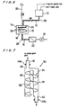
- FIGS. 1 through 3 The components or elements shown in FIGS. 1 through 3 which are identical or similar to the components or elements in the conventional apparatus shown in FIG. 7 are designated using the same reference numerals.
- FIG. 1 shows a trap apparatus
- the trap apparatus 30 comprises a trap container 36 having a cylindrical cup-shaped body for defining a trap chamber therein, an inlet pipe 38 connected to the side surface of the trap container 36, and an outlet pipe 40 connected to the other side surface of the trap container 36.
- a cooling device 50 is disposed in the trap container 36 to cool an interior atmosphere of the trap container 36, and the upper open end of the trap container 36 is closed by a lid 52.
- the cooling device 50 serves not only to solidify components having a low vapor pressure such as unreacted material gas but also to cool components which are relatively easily liquidized to a temperature so as to be condensed or lower.
- the cooling device 50 uses liquid nitrogen in this example, and has a vessel 54 for storing liquid nitrogen, a liquid nitrogen supply pipe 56 for supplying liquid nitrogen into the vessel 54, and a discharge pipe 58.
- the vessel 54 has a number of fins 60 on the outer surface thereof.
- the fins 60 are cooled to a temperature of approximately -176°C corresponding to the boiling point of liquid nitrogen.
- the trap apparatus 30 is provided in the evacuation passage 16 which interconnects the reaction chamber 14 and the vacuum pump 18, and gases discharged from the reaction chamber 14 are introduced into the trap container 36.
- the material gas supplied to the vapor deposition apparatus is produced by liquidizing Ba(DPM) 2 , Sr(DPM) 2 or the like which is solid at room temperature, adding an adduct for accelerating vaporization, mixing the liquidized substance with organic solvent, and vaporizing the obtained mixture. Therefore, gases discharged from the reaction chamber 14 contain components having a low vapor pressure such as unconsumed material or reaction by-product, a solvent gas contained in the material gas, an adduct gas of material, and a carriage gas.
- butyl acetate, tetrahydrofuran, lutidine, or the like is used, and as an adduct, tetraglymes, toluenes, tetraenes, or the like is used.
- the discharged gases containing various substances are introduced into the trap container 36, and the components having a low vapor pressure such as the unconsumed material or the reaction by-product are solidified and deposited on the inner surface of the trap container 36 and the outer surfaces of the fins 60 of the cooling device 50.
- gas components such as a solvent or an adduct which are easily liquidized are condensed, and hence they are also contained in the deposited substances.
- the deposited substances in the trap container 36 become moist. Therefore, adhesion between the deposited substances and the inner surface of the trap container and cohesion of the deposited substances are heighten, and hence the deposited substances are prevented from being removed from the inner surface of the trap container 36 and the surfaces of the fins 60, thus preventing generation of particles.
- FIG. 2 shows another trap apparatus.
- the trap apparatus is different from the previously described trap apparatus in that the cooling device 50 using liquid nitrogen is replaced with a GM (Gifford-McMahon) cycle helium refrigerator 62.
- the GM cycle helium refrigerator 62 has such a structure that cold panels 68 provided in a refrigerating unit 64 are cooled by supplying liquid helium from the compressor 66 to the refrigerating unit 64.
- the open end of the trap container 36 is closed by a flange 70 of the refrigerating unit 64.
- the interior atmosphere in the trap apparatus 36 can be cooled to a temperature equal to or lower than the condensing temperature of the solvent gas contained in the material gas or the adduct gas of material.
- FIG. 3 shows a trap apparatus according to a first embodiment of the present invention.
- the trap apparatus in this embodiment has a two-stage trap structure. This structure is applicable to the case where material itself has a low vapor pressure and can be trapped by natural heat dissipation.
- the trap container 36 in the trap apparatus 30 has a solvent storage 76 disposed at a lower portion thereof for storing a solvent 74, which is hard to be volatilized, in a liquid state.
- the solvent storage 76 is enclosed by a cooling jacket 72 through which cooling medium flows.
- a liquid level sensor 78 for detecting a liquid level of the solvent 74
- a temperature sensor 80 for detecting a temperature of the solvent 74.
- the solvent 74 may use a solvent such as butyl acetate which is used as a solvent of material, a solvent such as tetraglymes which is used as an adduct of material, or a solvent such as dipivaloylmethane which is used as a ligand of material.
- a solvent such as butyl acetate which is used as a solvent of material
- a solvent such as tetraglymes which is used as an adduct of material
- a solvent such as dipivaloylmethane which is used as a ligand of material.
- the interior of the trap container 36 is divided by a partition plate 82 having a lower end extending to a position lower than the liquid level of the solvent 74 into a first chamber 84a and a second chamber 84b.
- An inlet pipe 38 is connected to the upper end of the first chamber 84a and an outlet pipe 40 is connected to the upper end of the second chamber 84b.
- the inlet pipe 38 has a lower end connected to an inner pipe 86 which extends downwardly in the first chamber 84a.
- the partition plate 82 has a communication opening 82a, at an upper portion thereof, where a communication pipe 88 extending downwardly in the second chamber 84b is connected to the partition plate 82.
- the trap apparatus 30 includes a solvent supply device 90 for supplying the solvent 74 into the trap container 36 periodically or irregularly.
- the solvent supply device 90 comprises a solvent tank 92 for storing the solvent 74, and a solvent supply line 96 extending from the solvent tank 92 and having a solvent supply pump 94 thereon.
- the solvent supply line 96 is branched into a line extending to the first chamber 84a and a line extending to the second chamber 84b, and both of the lines are connected to respective sprays 98 located in the first chamber 84a and the second chamber 84b, respectively.
- the solvent tank 92 is connected to the solvent storage 76 in the trap container 36 through a recovery line 102 having a valve 100 thereon.
- the solvent supply pump 94 the solvent 74 stored in the solvent tank 92 is supplied from the sprays 98 into the first chamber 84a and the second chamber 84b in the trap container 36.
- gases discharged from the reaction chamber 14 are introduced into the first chamber 84a in the trap container 36 through the inlet pipe 38, and flow upwardly in the first chamber 84a.
- components having a low vapor pressure such as unconsumed material are cooled by natural heat dissipation and condensed, and fall due to inertia of the flow, and are then trapped by the solvent 74 stored in the solvent storage 76.
- the gases which have flowed upwardly in the first chamber 84a flow downwardly in the communication pipe 88, and then are introduced into the second chamber 84b.
- components having a low vapor pressure such as unconsumed material are cooled by natural heat dissipation and trapped by the solvent 74 stored in the solvent storage 76.
- the temperature of the solvent 74 in the solvent storage 76 is controlled to a value so as not to progress vaporization of components having a low vapor pressure.
- the components having a low vapor pressure solidified in the first chamber 84a and the second chamber 84b are deposited party on the inner surface of the trap container 36, and the surfaces of partition plate 82, the inner pipe 86 and the communication pipe 88. Therefore, the solvent supply pump 94 of the solvent supply device 90 is operated periodically or irregularly, and the solvent 74 stored in the solvent tank 92 is sprayed from the sprays 98 into the first chamber 84a and the second chamber 84b.
- the components having a low vapor pressure and deposited on the inner surface of the trap container 36, the surface of the partition plate 82 and the like are moistened by the solvent 74, and hence adhesion between the deposited substances and the inner surface of the container and the like and cohesion of the deposited substances are heighten, and the deposited substances are prevented from being removed from the inner surface of the trap container 36, the surface of the partition plate 82 and the like.
- the liquid level of the solvent 74 in the solvent storage 76 can be adjusted by adjusting the amount of the solvent 74 supplied from the sprays 98 and the amount of the solvent 74 discharged from the solvent storage 76. Further, if the concentration of material in the solvent 74 stored in the solvent storage 76 becomes high, then the solvent 74 in the solvent storage 76 is replaced with a new one, and trapping operation can be continued.
- the solvent 74 in the case where a solvent such as butyl acetate which is used as a solvent of material, a solvent such as dipivaloylmethane which is used as a ligand of material, or a solvent such as tetraglymes which is used as an adduct of material is utilized, even if the solvent 74 is vaporized and flows back into the reaction chamber 14, the solvent is prevented from being contained in the thin film deposited on the substrate, thus preventing detrioration of quality of the film.
- a solvent such as butyl acetate which is used as a solvent of material
- a solvent such as dipivaloylmethane which is used as a ligand of material
- a solvent such as tetraglymes which is used as an adduct of material
- FIG. 4 shows a modified embodiment of the first embodiment shown in FIG. 3.
- the solvent 74 which is hard to be volatilized, is supplied directly to the solvent storage 76 without passing through the sprays 98.
- the solvent supply pump 94 is controlled by a controller (not shown) so that the liquid level of the solvent 74 is kept to form a clearance ⁇ having a certain small value between the liquid level, and the inner pipe 86 and the communication pipe 88.
- This structure allows the discharged gases to collide with solvent 74, and the components having a low vapor pressure in the gases are trapped directly by the solvent 74.
- scattering of the deposited substances is hard to occur, compared with the conventional trap apparatus incorporating the baffle plate 32 shown in FIG. 7.
- FIG. 5 shows a trap apparatus according to still another embodiment of the present invention.
- a plurality of trays 100a, 100b, 100c, 100d and 100e whose diameters are gradually larger downwardly are provided in a multi-stage manner.
- the solvent 74 which is hard to be vaporized, is supplied to the uppermost tray 100a from a storage tank 92 by a pump 94 through a supply pipe 104 extending upwardly at a central portion of the container 36, and then supplied to the lower trays 100b to 100e in sequence in order of height by overflow, thus constructing multi-stage cascades.
- the discharged gases are introduced into the container 36 through the inlet pipe 38 provided at the central and upper portion of the trap container, pass through a discharge opening 106 positioned at the outer circumferential portion of the trap container 36 and immediately above the liquid level of the solvent 74, and are then discharged from the trap container 36 through the outlet pipe 40.
- the solvent 74 which is hard to be vaporized, is circulated between the interior of the trap container 36 and the external storage tank 92, and purified by filters 108 and reused.
- liquid levels and cascades are provided in a multi-stage manner to increase trap efficiency, and the trapped substances are removed with the filter 108 by circulating the solvent 74 and discharged to the exterior of the system.
- the timing of replacement of the filter 108 may be judged by detecting a rise of the liquid level of the solvent in the trap apparatus 30 for thereby estimating resistance of the filter.
- gases which are easily liguidized, such as a solvent gas contained in a material gas are condensed in the trap container, or substances which are hard to be volatilized are supplied to the trap container, and deposited substances in the trap container are moistened, and hence adhesion between the deposited substances and the inner surface of the trap container and cohesion of the deposited substances are heighten.
- the deposited substances are prevented from being removed from the inner surface of the trap container and the like, thus preventing generation of particles. Therefore, components having a low vapor pressure in the discharge gases can be trapped reliably and scattering of the trapped substances can be prevented.
- a process chamber such as a reaction chamber positioned at the preceding stage, a process such as deposition can be carried out smoothly and in a high quality, and hence the present invention offers a useful technology in the semiconductor manufacturing industry.
Landscapes
- Chemical & Material Sciences (AREA)
- Chemical Kinetics & Catalysis (AREA)
- General Chemical & Material Sciences (AREA)
- Engineering & Computer Science (AREA)
- Materials Engineering (AREA)
- Mechanical Engineering (AREA)
- Metallurgy (AREA)
- Organic Chemistry (AREA)
- Chemical Vapour Deposition (AREA)
- Compressors, Vaccum Pumps And Other Relevant Systems (AREA)
Claims (7)
- Eine Fallenvorrichtung zur Verwendung mit einer Vakuumprozesskammer (14) zum Prozessieren eines Substrats, wobei die Fallenvorrichtung stromabwärts bezüglich der Vakuumprozesskammer angeordnet ist und betriebsmäßig eine Komponente mit einem niedrigen Dampfdruck einfängt, die in einem Gas enthalten ist, das aus der Vakuumprozesskammer ausgegeben wird, wobei die Fallenvorrichtung Folgendes aufweist:einen Fallenbehälter (36) zum Aufnehmen des von der Vakuumprozesskammer ausgegebenen Gases;eine Lösungsmittelversorgungsvorrichtung (90) zum Liefern eines Lösungsmittels in den Fallenbehälter (36), wobei das Lösungsmittel einen flüssigen Zustand unter den Unterdruckbedingungen in dem Fallenbehälter beibehält, um zu erlauben, dass das Lösungsmittel die Komponente mit dem niedrigen Dampfdruck befeuchtet und einfängt; undeine Lösungsmittelkühlvorrichtung (72) zum Kühlen des Lösungsmittels zum Kondensieren der Komponente mit dem niedrigen Dampfdruck.
- Fallenvorrichtung nach Anspruch 1, wobei die Fallenvorrichtung ferner Folgendes aufweist:einen Lösungsmittelspeicher (76), der in dem Fallenbehälter vorgesehen ist zum Speichern des schwer zu verdampfenden Lösungsmittels in einem flüssigen Zustand.
- Fallenvorrichtung nach Anspruch 1, wobei das schwer zu verdampfende Lösungsmittel ausgewählt ist, aus einem Lösungsmittel, das verwendet wird als ein Lösungsmittelmaterial einschließlich Butylacetat, Tetrahydrofurane, Lutidin, ein Lösungsmittel, das verwendet wird als ein Materialzusatz einschließlich Tetraglyme, Toluene, Tetraene oder ein Lösungsmittel, das als ein Materialligant verwendet wird, einschließlich Dipivaloylmethan.
- Fallenvorrichtung nach einem der Ansprüche 1 bis 3, wobei die Kühlvorrichtung (72), die in dem Fallenbehälter vorgesehen ist zum Kühlen des Gases auf eine Temperatur dient, die gleich oder niedriger ist als eine Kondensiertemperatur einer Gaskomponente, die in dem Gas enthalten ist und leicht verflüssigt werden kann.
- Dünnfilmdampfabscheidungsvorrichtung, die Folgendes aufweist:einen Verdampfer (10) zum Verdampfen eines flüssigen Materials;eine Vakuumprozesskammer (14), die stromabwärts bezüglich des Verdampfers angeordnet ist;eine Vakuumpumpe (18), die stromabwärts bezüglich der Vakuumprozesskammer angeordnet ist; undeine Fallenvorrichtung, die in einem Evakuierungsdurchlass vorgesehen ist, der sich von der Vakuumprozesskammer zu der Vakuumpumpe erstreckt, wobei die Fallenvorrichtung einer Vorrichtung gemäß einem der Ansprüche 1 bis 4 ist.
- Verwendung einer Fallenvorrichtung in Kombination mit einer Vakuumprozesskammer für das Prozessieren eines Substrats, wobei die Fallenvorrichtung im Anspruch 1 definiert ist.
- Ein Verfahren zum Einfangen einer Komponente mit einem niedrigen Dampfdruck, die in einem Abgas von einer Prozesskammer zum Prozessieren eines Substrats enthalten ist, in einer Fallenvorrichtung (34), wobei das Verfahren die folgenden Schritte aufweist:Liefern eines Lösungsmittels in einem Fallenbehälter (36) mittels einer Lösungsmittelversorgungsvorrichtung (90), wobei das Lösungsmittel einen flüssigen Zustand unter den Unterdruckbedingungen in dem Fallenbehälter beibehält, um zu ermöglichen, dass das Lösungsmittel die Komponente mit dem niedrigen Dampfdruck befeuchtet und einfängt;Kühlen des Lösungsmittels durch eine Kühlvorrichtung (72) zum Kondensieren der Komponente mit dem niedrigen Dampfdruck; undEinfangen der Komponente, die einen niedrigen Dampfdruck aufweist und in dem Gas enthalten ist mittels des flüssigen Lösungsmittels.
Applications Claiming Priority (2)
| Application Number | Priority Date | Filing Date | Title |
|---|---|---|---|
| JP11050610A JP2000249058A (ja) | 1999-02-26 | 1999-02-26 | トラップ装置 |
| JP5061099 | 1999-02-26 |
Publications (4)
| Publication Number | Publication Date |
|---|---|
| EP1031640A1 EP1031640A1 (de) | 2000-08-30 |
| EP1031640B1 EP1031640B1 (de) | 2006-08-09 |
| EP1031640B8 EP1031640B8 (de) | 2006-12-13 |
| EP1031640B9 true EP1031640B9 (de) | 2007-02-28 |
Family
ID=12863752
Family Applications (1)
| Application Number | Title | Priority Date | Filing Date |
|---|---|---|---|
| EP00103982A Expired - Lifetime EP1031640B9 (de) | 1999-02-26 | 2000-02-25 | Falle |
Country Status (6)
| Country | Link |
|---|---|
| US (1) | US6488774B1 (de) |
| EP (1) | EP1031640B9 (de) |
| JP (1) | JP2000249058A (de) |
| KR (1) | KR100653828B1 (de) |
| DE (1) | DE60029856T2 (de) |
| TW (1) | TW498132B (de) |
Families Citing this family (316)
| Publication number | Priority date | Publication date | Assignee | Title |
|---|---|---|---|---|
| JP3448644B2 (ja) | 2000-10-26 | 2003-09-22 | 名古屋大学長 | 真空排気兼不活性ガス導入装置 |
| US7780785B2 (en) * | 2001-10-26 | 2010-08-24 | Applied Materials, Inc. | Gas delivery apparatus for atomic layer deposition |
| US20080206445A1 (en) * | 2007-02-22 | 2008-08-28 | John Peck | Selective separation processes |
| DE112007000541T5 (de) * | 2006-03-14 | 2009-01-22 | Praxair Technology, Inc., Danbury | Selektive Trennverfahren |
| US8370711B2 (en) | 2008-06-23 | 2013-02-05 | Ramot At Tel Aviv University Ltd. | Interruption criteria for block decoding |
| US9394608B2 (en) | 2009-04-06 | 2016-07-19 | Asm America, Inc. | Semiconductor processing reactor and components thereof |
| US8802201B2 (en) | 2009-08-14 | 2014-08-12 | Asm America, Inc. | Systems and methods for thin-film deposition of metal oxides using excited nitrogen-oxygen species |
| US20130023129A1 (en) | 2011-07-20 | 2013-01-24 | Asm America, Inc. | Pressure transmitter for a semiconductor processing environment |
| US9017481B1 (en) | 2011-10-28 | 2015-04-28 | Asm America, Inc. | Process feed management for semiconductor substrate processing |
| JP5877702B2 (ja) * | 2011-12-14 | 2016-03-08 | 株式会社ニューフレアテクノロジー | 成膜装置および成膜方法 |
| US10714315B2 (en) | 2012-10-12 | 2020-07-14 | Asm Ip Holdings B.V. | Semiconductor reaction chamber showerhead |
| US20160376700A1 (en) | 2013-02-01 | 2016-12-29 | Asm Ip Holding B.V. | System for treatment of deposition reactor |
| US11015245B2 (en) | 2014-03-19 | 2021-05-25 | Asm Ip Holding B.V. | Gas-phase reactor and system having exhaust plenum and components thereof |
| US10858737B2 (en) | 2014-07-28 | 2020-12-08 | Asm Ip Holding B.V. | Showerhead assembly and components thereof |
| US9890456B2 (en) | 2014-08-21 | 2018-02-13 | Asm Ip Holding B.V. | Method and system for in situ formation of gas-phase compounds |
| US10941490B2 (en) | 2014-10-07 | 2021-03-09 | Asm Ip Holding B.V. | Multiple temperature range susceptor, assembly, reactor and system including the susceptor, and methods of using the same |
| US10276355B2 (en) | 2015-03-12 | 2019-04-30 | Asm Ip Holding B.V. | Multi-zone reactor, system including the reactor, and method of using the same |
| US10458018B2 (en) | 2015-06-26 | 2019-10-29 | Asm Ip Holding B.V. | Structures including metal carbide material, devices including the structures, and methods of forming same |
| US10211308B2 (en) | 2015-10-21 | 2019-02-19 | Asm Ip Holding B.V. | NbMC layers |
| US11139308B2 (en) | 2015-12-29 | 2021-10-05 | Asm Ip Holding B.V. | Atomic layer deposition of III-V compounds to form V-NAND devices |
| US10529554B2 (en) | 2016-02-19 | 2020-01-07 | Asm Ip Holding B.V. | Method for forming silicon nitride film selectively on sidewalls or flat surfaces of trenches |
| US10343920B2 (en) | 2016-03-18 | 2019-07-09 | Asm Ip Holding B.V. | Aligned carbon nanotubes |
| US10190213B2 (en) | 2016-04-21 | 2019-01-29 | Asm Ip Holding B.V. | Deposition of metal borides |
| US10865475B2 (en) | 2016-04-21 | 2020-12-15 | Asm Ip Holding B.V. | Deposition of metal borides and silicides |
| US10367080B2 (en) | 2016-05-02 | 2019-07-30 | Asm Ip Holding B.V. | Method of forming a germanium oxynitride film |
| US11453943B2 (en) | 2016-05-25 | 2022-09-27 | Asm Ip Holding B.V. | Method for forming carbon-containing silicon/metal oxide or nitride film by ALD using silicon precursor and hydrocarbon precursor |
| US9859151B1 (en) | 2016-07-08 | 2018-01-02 | Asm Ip Holding B.V. | Selective film deposition method to form air gaps |
| US10612137B2 (en) | 2016-07-08 | 2020-04-07 | Asm Ip Holdings B.V. | Organic reactants for atomic layer deposition |
| KR102532607B1 (ko) | 2016-07-28 | 2023-05-15 | 에이에스엠 아이피 홀딩 비.브이. | 기판 가공 장치 및 그 동작 방법 |
| US9812320B1 (en) | 2016-07-28 | 2017-11-07 | Asm Ip Holding B.V. | Method and apparatus for filling a gap |
| US9887082B1 (en) | 2016-07-28 | 2018-02-06 | Asm Ip Holding B.V. | Method and apparatus for filling a gap |
| US10643826B2 (en) | 2016-10-26 | 2020-05-05 | Asm Ip Holdings B.V. | Methods for thermally calibrating reaction chambers |
| US11532757B2 (en) | 2016-10-27 | 2022-12-20 | Asm Ip Holding B.V. | Deposition of charge trapping layers |
| US10229833B2 (en) | 2016-11-01 | 2019-03-12 | Asm Ip Holding B.V. | Methods for forming a transition metal nitride film on a substrate by atomic layer deposition and related semiconductor device structures |
| US10714350B2 (en) | 2016-11-01 | 2020-07-14 | ASM IP Holdings, B.V. | Methods for forming a transition metal niobium nitride film on a substrate by atomic layer deposition and related semiconductor device structures |
| KR102546317B1 (ko) | 2016-11-15 | 2023-06-21 | 에이에스엠 아이피 홀딩 비.브이. | 기체 공급 유닛 및 이를 포함하는 기판 처리 장치 |
| KR102762543B1 (ko) | 2016-12-14 | 2025-02-05 | 에이에스엠 아이피 홀딩 비.브이. | 기판 처리 장치 |
| US11447861B2 (en) | 2016-12-15 | 2022-09-20 | Asm Ip Holding B.V. | Sequential infiltration synthesis apparatus and a method of forming a patterned structure |
| US11581186B2 (en) | 2016-12-15 | 2023-02-14 | Asm Ip Holding B.V. | Sequential infiltration synthesis apparatus |
| KR102700194B1 (ko) | 2016-12-19 | 2024-08-28 | 에이에스엠 아이피 홀딩 비.브이. | 기판 처리 장치 |
| US10269558B2 (en) | 2016-12-22 | 2019-04-23 | Asm Ip Holding B.V. | Method of forming a structure on a substrate |
| US10867788B2 (en) | 2016-12-28 | 2020-12-15 | Asm Ip Holding B.V. | Method of forming a structure on a substrate |
| US11390950B2 (en) | 2017-01-10 | 2022-07-19 | Asm Ip Holding B.V. | Reactor system and method to reduce residue buildup during a film deposition process |
| US10468261B2 (en) | 2017-02-15 | 2019-11-05 | Asm Ip Holding B.V. | Methods for forming a metallic film on a substrate by cyclical deposition and related semiconductor device structures |
| US10529563B2 (en) | 2017-03-29 | 2020-01-07 | Asm Ip Holdings B.V. | Method for forming doped metal oxide films on a substrate by cyclical deposition and related semiconductor device structures |
| KR102457289B1 (ko) | 2017-04-25 | 2022-10-21 | 에이에스엠 아이피 홀딩 비.브이. | 박막 증착 방법 및 반도체 장치의 제조 방법 |
| US10770286B2 (en) | 2017-05-08 | 2020-09-08 | Asm Ip Holdings B.V. | Methods for selectively forming a silicon nitride film on a substrate and related semiconductor device structures |
| US10892156B2 (en) | 2017-05-08 | 2021-01-12 | Asm Ip Holding B.V. | Methods for forming a silicon nitride film on a substrate and related semiconductor device structures |
| US10886123B2 (en) | 2017-06-02 | 2021-01-05 | Asm Ip Holding B.V. | Methods for forming low temperature semiconductor layers and related semiconductor device structures |
| US12040200B2 (en) | 2017-06-20 | 2024-07-16 | Asm Ip Holding B.V. | Semiconductor processing apparatus and methods for calibrating a semiconductor processing apparatus |
| US11306395B2 (en) | 2017-06-28 | 2022-04-19 | Asm Ip Holding B.V. | Methods for depositing a transition metal nitride film on a substrate by atomic layer deposition and related deposition apparatus |
| KR20190009245A (ko) | 2017-07-18 | 2019-01-28 | 에이에스엠 아이피 홀딩 비.브이. | 반도체 소자 구조물 형성 방법 및 관련된 반도체 소자 구조물 |
| US11374112B2 (en) | 2017-07-19 | 2022-06-28 | Asm Ip Holding B.V. | Method for depositing a group IV semiconductor and related semiconductor device structures |
| US11018002B2 (en) | 2017-07-19 | 2021-05-25 | Asm Ip Holding B.V. | Method for selectively depositing a Group IV semiconductor and related semiconductor device structures |
| US10541333B2 (en) | 2017-07-19 | 2020-01-21 | Asm Ip Holding B.V. | Method for depositing a group IV semiconductor and related semiconductor device structures |
| US10590535B2 (en) | 2017-07-26 | 2020-03-17 | Asm Ip Holdings B.V. | Chemical treatment, deposition and/or infiltration apparatus and method for using the same |
| TWI815813B (zh) | 2017-08-04 | 2023-09-21 | 荷蘭商Asm智慧財產控股公司 | 用於分配反應腔內氣體的噴頭總成 |
| US10770336B2 (en) | 2017-08-08 | 2020-09-08 | Asm Ip Holding B.V. | Substrate lift mechanism and reactor including same |
| US10692741B2 (en) | 2017-08-08 | 2020-06-23 | Asm Ip Holdings B.V. | Radiation shield |
| US11769682B2 (en) | 2017-08-09 | 2023-09-26 | Asm Ip Holding B.V. | Storage apparatus for storing cassettes for substrates and processing apparatus equipped therewith |
| US11139191B2 (en) | 2017-08-09 | 2021-10-05 | Asm Ip Holding B.V. | Storage apparatus for storing cassettes for substrates and processing apparatus equipped therewith |
| US11830730B2 (en) | 2017-08-29 | 2023-11-28 | Asm Ip Holding B.V. | Layer forming method and apparatus |
| US11295980B2 (en) | 2017-08-30 | 2022-04-05 | Asm Ip Holding B.V. | Methods for depositing a molybdenum metal film over a dielectric surface of a substrate by a cyclical deposition process and related semiconductor device structures |
| US11056344B2 (en) | 2017-08-30 | 2021-07-06 | Asm Ip Holding B.V. | Layer forming method |
| KR102491945B1 (ko) | 2017-08-30 | 2023-01-26 | 에이에스엠 아이피 홀딩 비.브이. | 기판 처리 장치 |
| KR102401446B1 (ko) | 2017-08-31 | 2022-05-24 | 에이에스엠 아이피 홀딩 비.브이. | 기판 처리 장치 |
| KR102630301B1 (ko) | 2017-09-21 | 2024-01-29 | 에이에스엠 아이피 홀딩 비.브이. | 침투성 재료의 순차 침투 합성 방법 처리 및 이를 이용하여 형성된 구조물 및 장치 |
| US10844484B2 (en) | 2017-09-22 | 2020-11-24 | Asm Ip Holding B.V. | Apparatus for dispensing a vapor phase reactant to a reaction chamber and related methods |
| US10658205B2 (en) | 2017-09-28 | 2020-05-19 | Asm Ip Holdings B.V. | Chemical dispensing apparatus and methods for dispensing a chemical to a reaction chamber |
| US10403504B2 (en) | 2017-10-05 | 2019-09-03 | Asm Ip Holding B.V. | Method for selectively depositing a metallic film on a substrate |
| US10923344B2 (en) | 2017-10-30 | 2021-02-16 | Asm Ip Holding B.V. | Methods for forming a semiconductor structure and related semiconductor structures |
| US10910262B2 (en) | 2017-11-16 | 2021-02-02 | Asm Ip Holding B.V. | Method of selectively depositing a capping layer structure on a semiconductor device structure |
| US11022879B2 (en) | 2017-11-24 | 2021-06-01 | Asm Ip Holding B.V. | Method of forming an enhanced unexposed photoresist layer |
| CN111316417B (zh) | 2017-11-27 | 2023-12-22 | 阿斯莫Ip控股公司 | 与批式炉偕同使用的用于储存晶圆匣的储存装置 |
| JP7206265B2 (ja) | 2017-11-27 | 2023-01-17 | エーエスエム アイピー ホールディング ビー.ブイ. | クリーン・ミニエンバイロメントを備える装置 |
| US10872771B2 (en) | 2018-01-16 | 2020-12-22 | Asm Ip Holding B. V. | Method for depositing a material film on a substrate within a reaction chamber by a cyclical deposition process and related device structures |
| CN111630203A (zh) | 2018-01-19 | 2020-09-04 | Asm Ip私人控股有限公司 | 通过等离子体辅助沉积来沉积间隙填充层的方法 |
| TWI799494B (zh) | 2018-01-19 | 2023-04-21 | 荷蘭商Asm 智慧財產控股公司 | 沈積方法 |
| US11018047B2 (en) | 2018-01-25 | 2021-05-25 | Asm Ip Holding B.V. | Hybrid lift pin |
| USD880437S1 (en) | 2018-02-01 | 2020-04-07 | Asm Ip Holding B.V. | Gas supply plate for semiconductor manufacturing apparatus |
| US11081345B2 (en) | 2018-02-06 | 2021-08-03 | Asm Ip Holding B.V. | Method of post-deposition treatment for silicon oxide film |
| US10896820B2 (en) | 2018-02-14 | 2021-01-19 | Asm Ip Holding B.V. | Method for depositing a ruthenium-containing film on a substrate by a cyclical deposition process |
| JP7124098B2 (ja) | 2018-02-14 | 2022-08-23 | エーエスエム・アイピー・ホールディング・ベー・フェー | 周期的堆積プロセスにより基材上にルテニウム含有膜を堆積させる方法 |
| US10731249B2 (en) | 2018-02-15 | 2020-08-04 | Asm Ip Holding B.V. | Method of forming a transition metal containing film on a substrate by a cyclical deposition process, a method for supplying a transition metal halide compound to a reaction chamber, and related vapor deposition apparatus |
| KR102636427B1 (ko) | 2018-02-20 | 2024-02-13 | 에이에스엠 아이피 홀딩 비.브이. | 기판 처리 방법 및 장치 |
| US10975470B2 (en) | 2018-02-23 | 2021-04-13 | Asm Ip Holding B.V. | Apparatus for detecting or monitoring for a chemical precursor in a high temperature environment |
| US11473195B2 (en) | 2018-03-01 | 2022-10-18 | Asm Ip Holding B.V. | Semiconductor processing apparatus and a method for processing a substrate |
| US11629406B2 (en) | 2018-03-09 | 2023-04-18 | Asm Ip Holding B.V. | Semiconductor processing apparatus comprising one or more pyrometers for measuring a temperature of a substrate during transfer of the substrate |
| US11114283B2 (en) | 2018-03-16 | 2021-09-07 | Asm Ip Holding B.V. | Reactor, system including the reactor, and methods of manufacturing and using same |
| KR102646467B1 (ko) | 2018-03-27 | 2024-03-11 | 에이에스엠 아이피 홀딩 비.브이. | 기판 상에 전극을 형성하는 방법 및 전극을 포함하는 반도체 소자 구조 |
| US11230766B2 (en) | 2018-03-29 | 2022-01-25 | Asm Ip Holding B.V. | Substrate processing apparatus and method |
| US11088002B2 (en) | 2018-03-29 | 2021-08-10 | Asm Ip Holding B.V. | Substrate rack and a substrate processing system and method |
| KR102501472B1 (ko) | 2018-03-30 | 2023-02-20 | 에이에스엠 아이피 홀딩 비.브이. | 기판 처리 방법 |
| KR102600229B1 (ko) | 2018-04-09 | 2023-11-10 | 에이에스엠 아이피 홀딩 비.브이. | 기판 지지 장치, 이를 포함하는 기판 처리 장치 및 기판 처리 방법 |
| KR102709511B1 (ko) | 2018-05-08 | 2024-09-24 | 에이에스엠 아이피 홀딩 비.브이. | 기판 상에 산화물 막을 주기적 증착 공정에 의해 증착하기 위한 방법 및 관련 소자 구조 |
| US12025484B2 (en) | 2018-05-08 | 2024-07-02 | Asm Ip Holding B.V. | Thin film forming method |
| US12272527B2 (en) | 2018-05-09 | 2025-04-08 | Asm Ip Holding B.V. | Apparatus for use with hydrogen radicals and method of using same |
| TWI816783B (zh) | 2018-05-11 | 2023-10-01 | 荷蘭商Asm 智慧財產控股公司 | 用於基板上形成摻雜金屬碳化物薄膜之方法及相關半導體元件結構 |
| KR102596988B1 (ko) | 2018-05-28 | 2023-10-31 | 에이에스엠 아이피 홀딩 비.브이. | 기판 처리 방법 및 그에 의해 제조된 장치 |
| TWI840362B (zh) | 2018-06-04 | 2024-05-01 | 荷蘭商Asm Ip私人控股有限公司 | 水氣降低的晶圓處置腔室 |
| US11718913B2 (en) | 2018-06-04 | 2023-08-08 | Asm Ip Holding B.V. | Gas distribution system and reactor system including same |
| US11286562B2 (en) | 2018-06-08 | 2022-03-29 | Asm Ip Holding B.V. | Gas-phase chemical reactor and method of using same |
| KR102568797B1 (ko) | 2018-06-21 | 2023-08-21 | 에이에스엠 아이피 홀딩 비.브이. | 기판 처리 시스템 |
| US10797133B2 (en) | 2018-06-21 | 2020-10-06 | Asm Ip Holding B.V. | Method for depositing a phosphorus doped silicon arsenide film and related semiconductor device structures |
| KR20250134000A (ko) | 2018-06-27 | 2025-09-09 | 에이에스엠 아이피 홀딩 비.브이. | 금속 함유 재료를 형성하기 위한 주기적 증착 방법 및 금속 함유 재료를 포함하는 필름 및 구조체 |
| US11499222B2 (en) | 2018-06-27 | 2022-11-15 | Asm Ip Holding B.V. | Cyclic deposition methods for forming metal-containing material and films and structures including the metal-containing material |
| KR102686758B1 (ko) | 2018-06-29 | 2024-07-18 | 에이에스엠 아이피 홀딩 비.브이. | 박막 증착 방법 및 반도체 장치의 제조 방법 |
| US10612136B2 (en) | 2018-06-29 | 2020-04-07 | ASM IP Holding, B.V. | Temperature-controlled flange and reactor system including same |
| US10755922B2 (en) | 2018-07-03 | 2020-08-25 | Asm Ip Holding B.V. | Method for depositing silicon-free carbon-containing film as gap-fill layer by pulse plasma-assisted deposition |
| US10388513B1 (en) | 2018-07-03 | 2019-08-20 | Asm Ip Holding B.V. | Method for depositing silicon-free carbon-containing film as gap-fill layer by pulse plasma-assisted deposition |
| US10767789B2 (en) | 2018-07-16 | 2020-09-08 | Asm Ip Holding B.V. | Diaphragm valves, valve components, and methods for forming valve components |
| US11053591B2 (en) | 2018-08-06 | 2021-07-06 | Asm Ip Holding B.V. | Multi-port gas injection system and reactor system including same |
| US10883175B2 (en) | 2018-08-09 | 2021-01-05 | Asm Ip Holding B.V. | Vertical furnace for processing substrates and a liner for use therein |
| US10829852B2 (en) | 2018-08-16 | 2020-11-10 | Asm Ip Holding B.V. | Gas distribution device for a wafer processing apparatus |
| US11430674B2 (en) | 2018-08-22 | 2022-08-30 | Asm Ip Holding B.V. | Sensor array, apparatus for dispensing a vapor phase reactant to a reaction chamber and related methods |
| US11024523B2 (en) | 2018-09-11 | 2021-06-01 | Asm Ip Holding B.V. | Substrate processing apparatus and method |
| KR102707956B1 (ko) | 2018-09-11 | 2024-09-19 | 에이에스엠 아이피 홀딩 비.브이. | 박막 증착 방법 |
| US11049751B2 (en) | 2018-09-14 | 2021-06-29 | Asm Ip Holding B.V. | Cassette supply system to store and handle cassettes and processing apparatus equipped therewith |
| CN110970344B (zh) | 2018-10-01 | 2024-10-25 | Asmip控股有限公司 | 衬底保持设备、包含所述设备的系统及其使用方法 |
| US11232963B2 (en) | 2018-10-03 | 2022-01-25 | Asm Ip Holding B.V. | Substrate processing apparatus and method |
| KR102592699B1 (ko) | 2018-10-08 | 2023-10-23 | 에이에스엠 아이피 홀딩 비.브이. | 기판 지지 유닛 및 이를 포함하는 박막 증착 장치와 기판 처리 장치 |
| KR102546322B1 (ko) | 2018-10-19 | 2023-06-21 | 에이에스엠 아이피 홀딩 비.브이. | 기판 처리 장치 및 기판 처리 방법 |
| KR102605121B1 (ko) | 2018-10-19 | 2023-11-23 | 에이에스엠 아이피 홀딩 비.브이. | 기판 처리 장치 및 기판 처리 방법 |
| USD948463S1 (en) | 2018-10-24 | 2022-04-12 | Asm Ip Holding B.V. | Susceptor for semiconductor substrate supporting apparatus |
| US12378665B2 (en) | 2018-10-26 | 2025-08-05 | Asm Ip Holding B.V. | High temperature coatings for a preclean and etch apparatus and related methods |
| US11087997B2 (en) | 2018-10-31 | 2021-08-10 | Asm Ip Holding B.V. | Substrate processing apparatus for processing substrates |
| KR102748291B1 (ko) | 2018-11-02 | 2024-12-31 | 에이에스엠 아이피 홀딩 비.브이. | 기판 지지 유닛 및 이를 포함하는 기판 처리 장치 |
| US11572620B2 (en) | 2018-11-06 | 2023-02-07 | Asm Ip Holding B.V. | Methods for selectively depositing an amorphous silicon film on a substrate |
| US11031242B2 (en) | 2018-11-07 | 2021-06-08 | Asm Ip Holding B.V. | Methods for depositing a boron doped silicon germanium film |
| DE202018005256U1 (de) * | 2018-11-13 | 2020-02-14 | Leybold Gmbh | Abscheidesystem für Gase bei Hochvakuumeinrichtung |
| US10818758B2 (en) | 2018-11-16 | 2020-10-27 | Asm Ip Holding B.V. | Methods for forming a metal silicate film on a substrate in a reaction chamber and related semiconductor device structures |
| US10847366B2 (en) | 2018-11-16 | 2020-11-24 | Asm Ip Holding B.V. | Methods for depositing a transition metal chalcogenide film on a substrate by a cyclical deposition process |
| US12040199B2 (en) | 2018-11-28 | 2024-07-16 | Asm Ip Holding B.V. | Substrate processing apparatus for processing substrates |
| US11217444B2 (en) | 2018-11-30 | 2022-01-04 | Asm Ip Holding B.V. | Method for forming an ultraviolet radiation responsive metal oxide-containing film |
| KR102636428B1 (ko) | 2018-12-04 | 2024-02-13 | 에이에스엠 아이피 홀딩 비.브이. | 기판 처리 장치를 세정하는 방법 |
| US11158513B2 (en) | 2018-12-13 | 2021-10-26 | Asm Ip Holding B.V. | Methods for forming a rhenium-containing film on a substrate by a cyclical deposition process and related semiconductor device structures |
| JP7504584B2 (ja) | 2018-12-14 | 2024-06-24 | エーエスエム・アイピー・ホールディング・ベー・フェー | 窒化ガリウムの選択的堆積を用いてデバイス構造体を形成する方法及びそのためのシステム |
| TWI819180B (zh) | 2019-01-17 | 2023-10-21 | 荷蘭商Asm 智慧財產控股公司 | 藉由循環沈積製程於基板上形成含過渡金屬膜之方法 |
| KR102727227B1 (ko) | 2019-01-22 | 2024-11-07 | 에이에스엠 아이피 홀딩 비.브이. | 기판 처리 장치 |
| CN111524788B (zh) | 2019-02-01 | 2023-11-24 | Asm Ip私人控股有限公司 | 氧化硅的拓扑选择性膜形成的方法 |
| KR102638425B1 (ko) | 2019-02-20 | 2024-02-21 | 에이에스엠 아이피 홀딩 비.브이. | 기판 표면 내에 형성된 오목부를 충진하기 위한 방법 및 장치 |
| US11482533B2 (en) | 2019-02-20 | 2022-10-25 | Asm Ip Holding B.V. | Apparatus and methods for plug fill deposition in 3-D NAND applications |
| KR102626263B1 (ko) | 2019-02-20 | 2024-01-16 | 에이에스엠 아이피 홀딩 비.브이. | 처리 단계를 포함하는 주기적 증착 방법 및 이를 위한 장치 |
| TWI845607B (zh) | 2019-02-20 | 2024-06-21 | 荷蘭商Asm Ip私人控股有限公司 | 用來填充形成於基材表面內之凹部的循環沉積方法及設備 |
| TWI842826B (zh) | 2019-02-22 | 2024-05-21 | 荷蘭商Asm Ip私人控股有限公司 | 基材處理設備及處理基材之方法 |
| KR102762833B1 (ko) | 2019-03-08 | 2025-02-04 | 에이에스엠 아이피 홀딩 비.브이. | SiOCN 층을 포함한 구조체 및 이의 형성 방법 |
| KR102858005B1 (ko) | 2019-03-08 | 2025-09-09 | 에이에스엠 아이피 홀딩 비.브이. | 실리콘 질화물 층을 선택적으로 증착하는 방법, 및 선택적으로 증착된 실리콘 질화물 층을 포함하는 구조체 |
| KR102782593B1 (ko) | 2019-03-08 | 2025-03-14 | 에이에스엠 아이피 홀딩 비.브이. | SiOC 층을 포함한 구조체 및 이의 형성 방법 |
| JP2020167398A (ja) | 2019-03-28 | 2020-10-08 | エーエスエム・アイピー・ホールディング・ベー・フェー | ドアオープナーおよびドアオープナーが提供される基材処理装置 |
| KR102809999B1 (ko) | 2019-04-01 | 2025-05-19 | 에이에스엠 아이피 홀딩 비.브이. | 반도체 소자를 제조하는 방법 |
| US11447864B2 (en) | 2019-04-19 | 2022-09-20 | Asm Ip Holding B.V. | Layer forming method and apparatus |
| KR20200125453A (ko) | 2019-04-24 | 2020-11-04 | 에이에스엠 아이피 홀딩 비.브이. | 기상 반응기 시스템 및 이를 사용하는 방법 |
| KR102929471B1 (ko) | 2019-05-07 | 2026-02-20 | 에이에스엠 아이피 홀딩 비.브이. | 딥 튜브가 있는 화학물질 공급원 용기 |
| KR102869364B1 (ko) | 2019-05-07 | 2025-10-10 | 에이에스엠 아이피 홀딩 비.브이. | 비정질 탄소 중합체 막을 개질하는 방법 |
| CN110095575A (zh) * | 2019-05-08 | 2019-08-06 | 中国科学技术大学 | 混合气体中单一气体的富集纯化设备 |
| KR102929472B1 (ko) | 2019-05-10 | 2026-02-20 | 에이에스엠 아이피 홀딩 비.브이. | 표면 상에 재료를 증착하는 방법 및 본 방법에 따라 형성된 구조 |
| JP7598201B2 (ja) | 2019-05-16 | 2024-12-11 | エーエスエム・アイピー・ホールディング・ベー・フェー | ウェハボートハンドリング装置、縦型バッチ炉および方法 |
| JP7612342B2 (ja) | 2019-05-16 | 2025-01-14 | エーエスエム・アイピー・ホールディング・ベー・フェー | ウェハボートハンドリング装置、縦型バッチ炉および方法 |
| USD947913S1 (en) | 2019-05-17 | 2022-04-05 | Asm Ip Holding B.V. | Susceptor shaft |
| USD975665S1 (en) | 2019-05-17 | 2023-01-17 | Asm Ip Holding B.V. | Susceptor shaft |
| USD935572S1 (en) | 2019-05-24 | 2021-11-09 | Asm Ip Holding B.V. | Gas channel plate |
| USD922229S1 (en) | 2019-06-05 | 2021-06-15 | Asm Ip Holding B.V. | Device for controlling a temperature of a gas supply unit |
| KR20200141003A (ko) | 2019-06-06 | 2020-12-17 | 에이에스엠 아이피 홀딩 비.브이. | 가스 감지기를 포함하는 기상 반응기 시스템 |
| KR102918757B1 (ko) | 2019-06-10 | 2026-01-28 | 에이에스엠 아이피 홀딩 비.브이. | 석영 에피택셜 챔버를 세정하는 방법 |
| KR20200143254A (ko) | 2019-06-11 | 2020-12-23 | 에이에스엠 아이피 홀딩 비.브이. | 개질 가스를 사용하여 전자 구조를 형성하는 방법, 상기 방법을 수행하기 위한 시스템, 및 상기 방법을 사용하여 형성되는 구조 |
| USD944946S1 (en) | 2019-06-14 | 2022-03-01 | Asm Ip Holding B.V. | Shower plate |
| USD931978S1 (en) | 2019-06-27 | 2021-09-28 | Asm Ip Holding B.V. | Showerhead vacuum transport |
| KR102911421B1 (ko) | 2019-07-03 | 2026-01-12 | 에이에스엠 아이피 홀딩 비.브이. | 기판 처리 장치용 온도 제어 조립체 및 이를 사용하는 방법 |
| JP7499079B2 (ja) | 2019-07-09 | 2024-06-13 | エーエスエム・アイピー・ホールディング・ベー・フェー | 同軸導波管を用いたプラズマ装置、基板処理方法 |
| CN112216646B (zh) | 2019-07-10 | 2026-02-10 | Asmip私人控股有限公司 | 基板支撑组件及包括其的基板处理装置 |
| KR102895115B1 (ko) | 2019-07-16 | 2025-12-03 | 에이에스엠 아이피 홀딩 비.브이. | 기판 처리 장치 |
| KR102860110B1 (ko) | 2019-07-17 | 2025-09-16 | 에이에스엠 아이피 홀딩 비.브이. | 실리콘 게르마늄 구조를 형성하는 방법 |
| KR102955799B1 (ko) | 2019-07-17 | 2026-04-21 | 에이에스엠 아이피 홀딩 비.브이. | 라디칼 보조 점화 플라즈마 시스템 및 방법 |
| US11643724B2 (en) | 2019-07-18 | 2023-05-09 | Asm Ip Holding B.V. | Method of forming structures using a neutral beam |
| KR102903090B1 (ko) | 2019-07-19 | 2025-12-19 | 에이에스엠 아이피 홀딩 비.브이. | 토폴로지-제어된 비정질 탄소 중합체 막을 형성하는 방법 |
| TWI839544B (zh) | 2019-07-19 | 2024-04-21 | 荷蘭商Asm Ip私人控股有限公司 | 形成形貌受控的非晶碳聚合物膜之方法 |
| TWI851767B (zh) | 2019-07-29 | 2024-08-11 | 荷蘭商Asm Ip私人控股有限公司 | 用於利用n型摻雜物及/或替代摻雜物選擇性沉積以達成高摻雜物併入之方法 |
| CN112309899B (zh) | 2019-07-30 | 2025-11-14 | Asmip私人控股有限公司 | 基板处理设备 |
| CN112309900B (zh) | 2019-07-30 | 2025-11-04 | Asmip私人控股有限公司 | 基板处理设备 |
| KR20210015655A (ko) | 2019-07-30 | 2021-02-10 | 에이에스엠 아이피 홀딩 비.브이. | 기판 처리 장치 및 방법 |
| US11587815B2 (en) | 2019-07-31 | 2023-02-21 | Asm Ip Holding B.V. | Vertical batch furnace assembly |
| US11587814B2 (en) | 2019-07-31 | 2023-02-21 | Asm Ip Holding B.V. | Vertical batch furnace assembly |
| US11227782B2 (en) | 2019-07-31 | 2022-01-18 | Asm Ip Holding B.V. | Vertical batch furnace assembly |
| US12622218B2 (en) | 2019-07-31 | 2026-05-05 | Asm Ip Holding B.V. | Cassette lid opening device |
| CN112323048B (zh) | 2019-08-05 | 2024-02-09 | Asm Ip私人控股有限公司 | 用于化学源容器的液位传感器 |
| KR20210018761A (ko) | 2019-08-09 | 2021-02-18 | 에이에스엠 아이피 홀딩 비.브이. | 냉각 장치를 포함한 히터 어셈블리 및 이를 사용하는 방법 |
| USD965524S1 (en) | 2019-08-19 | 2022-10-04 | Asm Ip Holding B.V. | Susceptor support |
| USD965044S1 (en) | 2019-08-19 | 2022-09-27 | Asm Ip Holding B.V. | Susceptor shaft |
| JP7810514B2 (ja) | 2019-08-21 | 2026-02-03 | エーエスエム・アイピー・ホールディング・ベー・フェー | 成膜原料混合ガス生成装置及び成膜装置 |
| USD930782S1 (en) | 2019-08-22 | 2021-09-14 | Asm Ip Holding B.V. | Gas distributor |
| USD979506S1 (en) | 2019-08-22 | 2023-02-28 | Asm Ip Holding B.V. | Insulator |
| KR20210024423A (ko) | 2019-08-22 | 2021-03-05 | 에이에스엠 아이피 홀딩 비.브이. | 홀을 구비한 구조체를 형성하기 위한 방법 |
| USD940837S1 (en) | 2019-08-22 | 2022-01-11 | Asm Ip Holding B.V. | Electrode |
| USD949319S1 (en) | 2019-08-22 | 2022-04-19 | Asm Ip Holding B.V. | Exhaust duct |
| KR102928101B1 (ko) | 2019-08-23 | 2026-02-13 | 에이에스엠 아이피 홀딩 비.브이. | 비스(디에틸아미노)실란을 사용하여 peald에 의해 개선된 품질을 갖는 실리콘 산화물 막을 증착하기 위한 방법 |
| US11286558B2 (en) | 2019-08-23 | 2022-03-29 | Asm Ip Holding B.V. | Methods for depositing a molybdenum nitride film on a surface of a substrate by a cyclical deposition process and related semiconductor device structures including a molybdenum nitride film |
| CN112442674A (zh) | 2019-09-03 | 2021-03-05 | Asm Ip私人控股有限公司 | 用于沉积硫族化物膜的方法和设备以及包括膜的结构 |
| KR102806450B1 (ko) | 2019-09-04 | 2025-05-12 | 에이에스엠 아이피 홀딩 비.브이. | 희생 캡핑 층을 이용한 선택적 증착 방법 |
| KR102733104B1 (ko) | 2019-09-05 | 2024-11-22 | 에이에스엠 아이피 홀딩 비.브이. | 기판 처리 장치 |
| US12469693B2 (en) | 2019-09-17 | 2025-11-11 | Asm Ip Holding B.V. | Method of forming a carbon-containing layer and structure including the layer |
| US11562901B2 (en) | 2019-09-25 | 2023-01-24 | Asm Ip Holding B.V. | Substrate processing method |
| CN112593212B (zh) | 2019-10-02 | 2023-12-22 | Asm Ip私人控股有限公司 | 通过循环等离子体增强沉积工艺形成拓扑选择性氧化硅膜的方法 |
| TWI846953B (zh) | 2019-10-08 | 2024-07-01 | 荷蘭商Asm Ip私人控股有限公司 | 基板處理裝置 |
| US12428726B2 (en) | 2019-10-08 | 2025-09-30 | Asm Ip Holding B.V. | Gas injection system and reactor system including same |
| KR102948143B1 (ko) | 2019-10-08 | 2026-04-07 | 에이에스엠 아이피 홀딩 비.브이. | 활성 종을 이용하기 위한 가스 분배 어셈블리를 포함한 반응기 시스템 및 이를 사용하는 방법 |
| TWI846966B (zh) | 2019-10-10 | 2024-07-01 | 荷蘭商Asm Ip私人控股有限公司 | 形成光阻底層之方法及包括光阻底層之結構 |
| US12009241B2 (en) | 2019-10-14 | 2024-06-11 | Asm Ip Holding B.V. | Vertical batch furnace assembly with detector to detect cassette |
| TWI834919B (zh) | 2019-10-16 | 2024-03-11 | 荷蘭商Asm Ip私人控股有限公司 | 氧化矽之拓撲選擇性膜形成之方法 |
| US11637014B2 (en) | 2019-10-17 | 2023-04-25 | Asm Ip Holding B.V. | Methods for selective deposition of doped semiconductor material |
| KR102845724B1 (ko) | 2019-10-21 | 2025-08-13 | 에이에스엠 아이피 홀딩 비.브이. | 막을 선택적으로 에칭하기 위한 장치 및 방법 |
| US11996292B2 (en) | 2019-10-25 | 2024-05-28 | Asm Ip Holding B.V. | Methods for filling a gap feature on a substrate surface and related semiconductor structures |
| US11646205B2 (en) | 2019-10-29 | 2023-05-09 | Asm Ip Holding B.V. | Methods of selectively forming n-type doped material on a surface, systems for selectively forming n-type doped material, and structures formed using same |
| KR102890638B1 (ko) | 2019-11-05 | 2025-11-25 | 에이에스엠 아이피 홀딩 비.브이. | 도핑된 반도체 층을 갖는 구조체 및 이를 형성하기 위한 방법 및 시스템 |
| US11501968B2 (en) | 2019-11-15 | 2022-11-15 | Asm Ip Holding B.V. | Method for providing a semiconductor device with silicon filled gaps |
| KR102861314B1 (ko) | 2019-11-20 | 2025-09-17 | 에이에스엠 아이피 홀딩 비.브이. | 기판의 표면 상에 탄소 함유 물질을 증착하는 방법, 상기 방법을 사용하여 형성된 구조물, 및 상기 구조물을 형성하기 위한 시스템 |
| KR20210065848A (ko) | 2019-11-26 | 2021-06-04 | 에이에스엠 아이피 홀딩 비.브이. | 제1 유전체 표면과 제2 금속성 표면을 포함한 기판 상에 타겟 막을 선택적으로 형성하기 위한 방법 |
| CN112951697B (zh) | 2019-11-26 | 2025-07-29 | Asmip私人控股有限公司 | 基板处理设备 |
| CN120432376A (zh) | 2019-11-29 | 2025-08-05 | Asm Ip私人控股有限公司 | 基板处理设备 |
| CN120998766A (zh) | 2019-11-29 | 2025-11-21 | Asm Ip私人控股有限公司 | 基板处理设备 |
| JP7527928B2 (ja) | 2019-12-02 | 2024-08-05 | エーエスエム・アイピー・ホールディング・ベー・フェー | 基板処理装置、基板処理方法 |
| KR20210070898A (ko) | 2019-12-04 | 2021-06-15 | 에이에스엠 아이피 홀딩 비.브이. | 기판 처리 장치 |
| JP7703317B2 (ja) | 2019-12-17 | 2025-07-07 | エーエスエム・アイピー・ホールディング・ベー・フェー | 窒化バナジウム層および窒化バナジウム層を含む構造体を形成する方法 |
| KR102943768B1 (ko) | 2019-12-19 | 2026-03-26 | 에이에스엠 아이피 홀딩 비.브이. | 기판 상의 갭 피처를 충진하는 방법 및 이와 관련된 반도체 소자 구조 |
| TWI887322B (zh) | 2020-01-06 | 2025-06-21 | 荷蘭商Asm Ip私人控股有限公司 | 反應器系統、抬升銷、及處理方法 |
| TWI901623B (zh) | 2020-01-06 | 2025-10-21 | 荷蘭商Asm Ip私人控股有限公司 | 氣體供應總成以及閥板總成 |
| US11993847B2 (en) | 2020-01-08 | 2024-05-28 | Asm Ip Holding B.V. | Injector |
| KR102882467B1 (ko) | 2020-01-16 | 2025-11-05 | 에이에스엠 아이피 홀딩 비.브이. | 고 종횡비 피처를 형성하는 방법 |
| KR102675856B1 (ko) | 2020-01-20 | 2024-06-17 | 에이에스엠 아이피 홀딩 비.브이. | 박막 형성 방법 및 박막 표면 개질 방법 |
| TWI889744B (zh) | 2020-01-29 | 2025-07-11 | 荷蘭商Asm Ip私人控股有限公司 | 污染物捕集系統、及擋板堆疊 |
| TWI871421B (zh) | 2020-02-03 | 2025-02-01 | 荷蘭商Asm Ip私人控股有限公司 | 包括釩或銦層的裝置、結構及其形成方法、系統 |
| KR20210100010A (ko) | 2020-02-04 | 2021-08-13 | 에이에스엠 아이피 홀딩 비.브이. | 대형 물품의 투과율 측정을 위한 방법 및 장치 |
| US11776846B2 (en) | 2020-02-07 | 2023-10-03 | Asm Ip Holding B.V. | Methods for depositing gap filling fluids and related systems and devices |
| KR20210103953A (ko) | 2020-02-13 | 2021-08-24 | 에이에스엠 아이피 홀딩 비.브이. | 가스 분배 어셈블리 및 이를 사용하는 방법 |
| KR102916725B1 (ko) | 2020-02-13 | 2026-01-23 | 에이에스엠 아이피 홀딩 비.브이. | 수광 장치를 포함하는 기판 처리 장치 및 수광 장치의 교정 방법 |
| US11781243B2 (en) | 2020-02-17 | 2023-10-10 | Asm Ip Holding B.V. | Method for depositing low temperature phosphorous-doped silicon |
| TWI895326B (zh) | 2020-02-28 | 2025-09-01 | 荷蘭商Asm Ip私人控股有限公司 | 專用於零件清潔的系統 |
| TWI914330B (zh) | 2020-03-04 | 2026-02-11 | 荷蘭商Asm Ip私人控股有限公司 | 反應器系統、及對準夾具 |
| KR20210116240A (ko) | 2020-03-11 | 2021-09-27 | 에이에스엠 아이피 홀딩 비.브이. | 조절성 접합부를 갖는 기판 핸들링 장치 |
| KR20210116249A (ko) | 2020-03-11 | 2021-09-27 | 에이에스엠 아이피 홀딩 비.브이. | 록아웃 태그아웃 어셈블리 및 시스템 그리고 이의 사용 방법 |
| CN113394086A (zh) | 2020-03-12 | 2021-09-14 | Asm Ip私人控股有限公司 | 用于制造具有目标拓扑轮廓的层结构的方法 |
| US12173404B2 (en) | 2020-03-17 | 2024-12-24 | Asm Ip Holding B.V. | Method of depositing epitaxial material, structure formed using the method, and system for performing the method |
| KR102755229B1 (ko) | 2020-04-02 | 2025-01-14 | 에이에스엠 아이피 홀딩 비.브이. | 박막 형성 방법 |
| TWI887376B (zh) | 2020-04-03 | 2025-06-21 | 荷蘭商Asm Ip私人控股有限公司 | 半導體裝置的製造方法 |
| TWI888525B (zh) | 2020-04-08 | 2025-07-01 | 荷蘭商Asm Ip私人控股有限公司 | 用於選擇性蝕刻氧化矽膜之設備及方法 |
| KR20210128343A (ko) | 2020-04-15 | 2021-10-26 | 에이에스엠 아이피 홀딩 비.브이. | 크롬 나이트라이드 층을 형성하는 방법 및 크롬 나이트라이드 층을 포함하는 구조 |
| US11821078B2 (en) | 2020-04-15 | 2023-11-21 | Asm Ip Holding B.V. | Method for forming precoat film and method for forming silicon-containing film |
| US11996289B2 (en) | 2020-04-16 | 2024-05-28 | Asm Ip Holding B.V. | Methods of forming structures including silicon germanium and silicon layers, devices formed using the methods, and systems for performing the methods |
| KR102901748B1 (ko) | 2020-04-21 | 2025-12-17 | 에이에스엠 아이피 홀딩 비.브이. | 기판을 처리하기 위한 방법 |
| KR102866804B1 (ko) | 2020-04-24 | 2025-09-30 | 에이에스엠 아이피 홀딩 비.브이. | 냉각 가스 공급부를 포함한 수직형 배치 퍼니스 어셈블리 |
| KR102934380B1 (ko) | 2020-04-24 | 2026-03-05 | 에이에스엠 아이피 홀딩 비.브이. | 바나듐 보라이드 및 바나듐 포스파이드 층을 포함한 구조체를 형성하는 방법 |
| KR20210132612A (ko) | 2020-04-24 | 2021-11-04 | 에이에스엠 아이피 홀딩 비.브이. | 바나듐 화합물들을 안정화하기 위한 방법들 및 장치 |
| KR20210132600A (ko) | 2020-04-24 | 2021-11-04 | 에이에스엠 아이피 홀딩 비.브이. | 바나듐, 질소 및 추가 원소를 포함한 층을 증착하기 위한 방법 및 시스템 |
| US11898243B2 (en) | 2020-04-24 | 2024-02-13 | Asm Ip Holding B.V. | Method of forming vanadium nitride-containing layer |
| KR102783898B1 (ko) | 2020-04-29 | 2025-03-18 | 에이에스엠 아이피 홀딩 비.브이. | 고체 소스 전구체 용기 |
| KR20210134869A (ko) | 2020-05-01 | 2021-11-11 | 에이에스엠 아이피 홀딩 비.브이. | Foup 핸들러를 이용한 foup의 빠른 교환 |
| JP7726664B2 (ja) | 2020-05-04 | 2025-08-20 | エーエスエム・アイピー・ホールディング・ベー・フェー | 基板を処理するための基板処理システム |
| KR20210137395A (ko) | 2020-05-07 | 2021-11-17 | 에이에스엠 아이피 홀딩 비.브이. | 불소계 라디칼을 이용하여 반응 챔버의 인시츄 식각을 수행하기 위한 장치 및 방법 |
| JP7736446B2 (ja) | 2020-05-07 | 2025-09-09 | エーエスエム・アイピー・ホールディング・ベー・フェー | 同調回路を備える反応器システム |
| KR102788543B1 (ko) | 2020-05-13 | 2025-03-27 | 에이에스엠 아이피 홀딩 비.브이. | 반응기 시스템용 레이저 정렬 고정구 |
| TWI915365B (zh) | 2020-05-15 | 2026-02-21 | 荷蘭商Asm Ip私人控股有限公司 | 形成矽鍺層之方法、半導體結構、半導體裝置、形成沉積層之方法、及沉積系統 |
| TWI911214B (zh) | 2020-05-19 | 2026-01-11 | 荷蘭商Asm Ip私人控股有限公司 | 基材處理設備 |
| KR102795476B1 (ko) | 2020-05-21 | 2025-04-11 | 에이에스엠 아이피 홀딩 비.브이. | 다수의 탄소 층을 포함한 구조체 및 이를 형성하고 사용하는 방법 |
| KR20210145079A (ko) | 2020-05-21 | 2021-12-01 | 에이에스엠 아이피 홀딩 비.브이. | 기판을 처리하기 위한 플랜지 및 장치 |
| TWI873343B (zh) | 2020-05-22 | 2025-02-21 | 荷蘭商Asm Ip私人控股有限公司 | 用於在基材上形成薄膜之反應系統 |
| KR20210146802A (ko) | 2020-05-26 | 2021-12-06 | 에이에스엠 아이피 홀딩 비.브이. | 붕소 및 갈륨을 함유한 실리콘 게르마늄 층을 증착하는 방법 |
| TWI876048B (zh) | 2020-05-29 | 2025-03-11 | 荷蘭商Asm Ip私人控股有限公司 | 基板處理方法 |
| TW202212620A (zh) | 2020-06-02 | 2022-04-01 | 荷蘭商Asm Ip私人控股有限公司 | 處理基板之設備、形成膜之方法、及控制用於處理基板之設備之方法 |
| KR20210156219A (ko) | 2020-06-16 | 2021-12-24 | 에이에스엠 아이피 홀딩 비.브이. | 붕소를 함유한 실리콘 게르마늄 층을 증착하는 방법 |
| TWI908816B (zh) | 2020-06-24 | 2025-12-21 | 荷蘭商Asm Ip私人控股有限公司 | 形成含矽層之方法 |
| TWI873359B (zh) | 2020-06-30 | 2025-02-21 | 荷蘭商Asm Ip私人控股有限公司 | 基板處理方法 |
| TWI896694B (zh) | 2020-07-01 | 2025-09-11 | 荷蘭商Asm Ip私人控股有限公司 | 沉積方法、半導體結構、及沉積系統 |
| TW202202649A (zh) | 2020-07-08 | 2022-01-16 | 荷蘭商Asm Ip私人控股有限公司 | 基板處理方法 |
| TWI864307B (zh) | 2020-07-17 | 2024-12-01 | 荷蘭商Asm Ip私人控股有限公司 | 用於光微影之結構、方法與系統 |
| TWI878570B (zh) | 2020-07-20 | 2025-04-01 | 荷蘭商Asm Ip私人控股有限公司 | 用於沉積鉬層之方法及系統 |
| KR20220011092A (ko) | 2020-07-20 | 2022-01-27 | 에이에스엠 아이피 홀딩 비.브이. | 전이 금속층을 포함하는 구조체를 형성하기 위한 방법 및 시스템 |
| US12322591B2 (en) | 2020-07-27 | 2025-06-03 | Asm Ip Holding B.V. | Thin film deposition process |
| TW202605918A (zh) | 2020-08-11 | 2026-02-01 | 荷蘭商Asm Ip私人控股有限公司 | 閘極堆疊 |
| KR102915124B1 (ko) | 2020-08-14 | 2026-01-19 | 에이에스엠 아이피 홀딩 비.브이. | 기판 처리 방법 |
| US12040177B2 (en) | 2020-08-18 | 2024-07-16 | Asm Ip Holding B.V. | Methods for forming a laminate film by cyclical plasma-enhanced deposition processes |
| TWI911263B (zh) | 2020-08-25 | 2026-01-11 | 荷蘭商Asm Ip私人控股有限公司 | 清潔基板的方法、選擇性沉積的方法、及反應器系統 |
| US11725280B2 (en) | 2020-08-26 | 2023-08-15 | Asm Ip Holding B.V. | Method for forming metal silicon oxide and metal silicon oxynitride layers |
| TWI911265B (zh) | 2020-08-27 | 2026-01-11 | 荷蘭商Asm Ip私人控股有限公司 | 形成圖案化結構的方法、操控機械特性的方法、及裝置結構 |
| TWI904232B (zh) | 2020-09-10 | 2025-11-11 | 荷蘭商Asm Ip私人控股有限公司 | 沉積間隙填充流體之方法及相關系統和裝置 |
| USD990534S1 (en) | 2020-09-11 | 2023-06-27 | Asm Ip Holding B.V. | Weighted lift pin |
| KR20220036866A (ko) | 2020-09-16 | 2022-03-23 | 에이에스엠 아이피 홀딩 비.브이. | 실리콘 산화물 증착 방법 |
| USD1012873S1 (en) | 2020-09-24 | 2024-01-30 | Asm Ip Holding B.V. | Electrode for semiconductor processing apparatus |
| TWI889903B (zh) | 2020-09-25 | 2025-07-11 | 荷蘭商Asm Ip私人控股有限公司 | 基板處理方法 |
| US12009224B2 (en) | 2020-09-29 | 2024-06-11 | Asm Ip Holding B.V. | Apparatus and method for etching metal nitrides |
| CN114388427A (zh) | 2020-10-06 | 2022-04-22 | Asm Ip私人控股有限公司 | 用于在特征的侧壁上形成氮化硅的方法和系统 |
| KR20220045900A (ko) | 2020-10-06 | 2022-04-13 | 에이에스엠 아이피 홀딩 비.브이. | 실리콘 함유 재료를 증착하기 위한 증착 방법 및 장치 |
| CN114293174A (zh) | 2020-10-07 | 2022-04-08 | Asm Ip私人控股有限公司 | 气体供应单元和包括气体供应单元的衬底处理设备 |
| KR102855834B1 (ko) | 2020-10-14 | 2025-09-04 | 에이에스엠 아이피 홀딩 비.브이. | 단차형 구조 상에 재료를 증착하는 방법 |
| KR102873665B1 (ko) | 2020-10-15 | 2025-10-17 | 에이에스엠 아이피 홀딩 비.브이. | 반도체 소자의 제조 방법, 및 ether-cat을 사용하는 기판 처리 장치 |
| TW202217037A (zh) | 2020-10-22 | 2022-05-01 | 荷蘭商Asm Ip私人控股有限公司 | 沉積釩金屬的方法、結構、裝置及沉積總成 |
| TW202223136A (zh) | 2020-10-28 | 2022-06-16 | 荷蘭商Asm Ip私人控股有限公司 | 用於在基板上形成層之方法、及半導體處理系統 |
| TW202229620A (zh) | 2020-11-12 | 2022-08-01 | 特文特大學 | 沉積系統、用於控制反應條件之方法、沉積方法 |
| TW202229795A (zh) | 2020-11-23 | 2022-08-01 | 荷蘭商Asm Ip私人控股有限公司 | 具注入器之基板處理設備 |
| TW202235649A (zh) | 2020-11-24 | 2022-09-16 | 荷蘭商Asm Ip私人控股有限公司 | 填充間隙之方法與相關之系統及裝置 |
| KR20220076343A (ko) | 2020-11-30 | 2022-06-08 | 에이에스엠 아이피 홀딩 비.브이. | 기판 처리 장치의 반응 챔버 내에 배열되도록 구성된 인젝터 |
| KR20220077875A (ko) | 2020-12-02 | 2022-06-09 | 에이에스엠 아이피 홀딩 비.브이. | 샤워헤드 어셈블리용 세정 고정구 |
| US12255053B2 (en) | 2020-12-10 | 2025-03-18 | Asm Ip Holding B.V. | Methods and systems for depositing a layer |
| US12159788B2 (en) | 2020-12-14 | 2024-12-03 | Asm Ip Holding B.V. | Method of forming structures for threshold voltage control |
| US11946137B2 (en) | 2020-12-16 | 2024-04-02 | Asm Ip Holding B.V. | Runout and wobble measurement fixtures |
| TW202232639A (zh) | 2020-12-18 | 2022-08-16 | 荷蘭商Asm Ip私人控股有限公司 | 具有可旋轉台的晶圓處理設備 |
| KR20220090438A (ko) | 2020-12-22 | 2022-06-29 | 에이에스엠 아이피 홀딩 비.브이. | 전이금속 증착 방법 |
| TW202226899A (zh) | 2020-12-22 | 2022-07-01 | 荷蘭商Asm Ip私人控股有限公司 | 具匹配器的電漿處理裝置 |
| KR20220090435A (ko) | 2020-12-22 | 2022-06-29 | 에이에스엠 아이피 홀딩 비.브이. | 전구체 캡슐, 용기 및 방법 |
| JP2022104305A (ja) | 2020-12-28 | 2022-07-08 | エドワーズ株式会社 | 真空ポンプ及び制御装置 |
| USD981973S1 (en) | 2021-05-11 | 2023-03-28 | Asm Ip Holding B.V. | Reactor wall for substrate processing apparatus |
| USD1023959S1 (en) | 2021-05-11 | 2024-04-23 | Asm Ip Holding B.V. | Electrode for substrate processing apparatus |
| USD980813S1 (en) | 2021-05-11 | 2023-03-14 | Asm Ip Holding B.V. | Gas flow control plate for substrate processing apparatus |
| USD980814S1 (en) | 2021-05-11 | 2023-03-14 | Asm Ip Holding B.V. | Gas distributor for substrate processing apparatus |
| USD990441S1 (en) | 2021-09-07 | 2023-06-27 | Asm Ip Holding B.V. | Gas flow control plate |
| USD1099184S1 (en) | 2021-11-29 | 2025-10-21 | Asm Ip Holding B.V. | Weighted lift pin |
| USD1060598S1 (en) | 2021-12-03 | 2025-02-04 | Asm Ip Holding B.V. | Split showerhead cover |
| KR102601305B1 (ko) * | 2022-12-27 | 2023-11-14 | 크라이오에이치앤아이(주) | 공정가스 제거 장치 |
Family Cites Families (22)
| Publication number | Priority date | Publication date | Assignee | Title |
|---|---|---|---|---|
| US4039307A (en) * | 1976-02-13 | 1977-08-02 | Envirotech Corporation | Countercurrent flow horizontal spray absorber |
| US4251236A (en) * | 1977-11-17 | 1981-02-17 | Ciba-Geigy Corporation | Process for purifying the off-gases from industrial furnaces, especially from waste incineration plants |
| JPS60241918A (ja) | 1984-05-16 | 1985-11-30 | Stanley Electric Co Ltd | アモルフアス・シリコン成膜プロセス中に副生成物として発生する粉塵の処理方法および装置 |
| FR2610215B1 (fr) * | 1987-02-03 | 1989-05-05 | Air Ind Systemes Sa | Dispositif de lavage d'un gaz pollue |
| US4963329A (en) * | 1987-03-02 | 1990-10-16 | Turbotak Inc. | Gas reacting apparatus and method |
| US4865817A (en) * | 1987-03-02 | 1989-09-12 | University Of Waterloo | Gas reacting apparatus |
| EP0382984A1 (de) * | 1989-02-13 | 1990-08-22 | L'air Liquide, Societe Anonyme Pour L'etude Et L'exploitation Des Procedes Georges Claude | Falle für thermische Zersetzung |
| US5011520A (en) * | 1989-12-15 | 1991-04-30 | Vector Technical Group, Inc. | Hydrodynamic fume scrubber |
| US5512072A (en) * | 1994-12-05 | 1996-04-30 | General Electric Environmental Services, Inc. | Flue gas scrubbing apparatus |
| US5653806A (en) | 1995-03-10 | 1997-08-05 | Advanced Technology Materials, Inc. | Showerhead-type discharge assembly for delivery of source reagent vapor to a substrate, and CVD process utilizing same |
| JP3287730B2 (ja) | 1995-04-20 | 2002-06-04 | 東京エレクトロン株式会社 | 混入物の除去装置、これを用いた処理装置の真空排気系及びそのメンテナンス方法 |
| JP3246708B2 (ja) * | 1995-05-02 | 2002-01-15 | 東京エレクトロン株式会社 | トラップ装置及びこれを用いた未反応処理ガス排気機構 |
| US5817575A (en) * | 1996-01-30 | 1998-10-06 | Advanced Micro Devices, Inc. | Prevention of clogging in CVD apparatus |
| KR100211649B1 (ko) * | 1996-02-29 | 1999-08-02 | 윤종용 | 반도체 lpcvd장비의 콜드트랩 |
| US5851293A (en) * | 1996-03-29 | 1998-12-22 | Atmi Ecosys Corporation | Flow-stabilized wet scrubber system for treatment of process gases from semiconductor manufacturing operations |
| KR100228768B1 (ko) | 1996-10-02 | 1999-11-01 | 김영환 | 화학 기상증착 장치 및 증착방법 |
| US5950925A (en) | 1996-10-11 | 1999-09-14 | Ebara Corporation | Reactant gas ejector head |
| US6051053A (en) | 1996-12-16 | 2000-04-18 | Ebara Corporation | Trapping device and method of operation therefor |
| US6068686A (en) * | 1997-10-07 | 2000-05-30 | Sorensen; Ian W. | Scrubber system and method of removing pollutants from a fluid |
| US6036756A (en) * | 1998-01-13 | 2000-03-14 | The Babcock & Wilcox Company | Retrofit of a center inlet type scrubber with absorption/gas distribution tray to improve gas-liquid contact in the absorption zone |
| US6106792A (en) * | 1998-03-30 | 2000-08-22 | L&P Property Management Company | Apparatus and method for cleaning gas |
| KR100282048B1 (ko) * | 1998-07-23 | 2001-02-15 | 윤장진 | 차량용 음성인식기의 웨이브파일 자동 분류 방법 |
-
1999
- 1999-02-26 JP JP11050610A patent/JP2000249058A/ja active Pending
-
2000
- 2000-02-24 US US09/512,333 patent/US6488774B1/en not_active Expired - Fee Related
- 2000-02-25 EP EP00103982A patent/EP1031640B9/de not_active Expired - Lifetime
- 2000-02-25 DE DE60029856T patent/DE60029856T2/de not_active Expired - Fee Related
- 2000-02-25 KR KR1020000009294A patent/KR100653828B1/ko not_active Expired - Fee Related
- 2000-02-25 TW TW089103338A patent/TW498132B/zh not_active IP Right Cessation
Also Published As
| Publication number | Publication date |
|---|---|
| EP1031640B1 (de) | 2006-08-09 |
| KR100653828B1 (ko) | 2006-12-04 |
| US6488774B1 (en) | 2002-12-03 |
| KR20010006697A (ko) | 2001-01-26 |
| TW498132B (en) | 2002-08-11 |
| JP2000249058A (ja) | 2000-09-12 |
| DE60029856D1 (de) | 2006-09-21 |
| DE60029856T2 (de) | 2007-03-08 |
| EP1031640A1 (de) | 2000-08-30 |
| EP1031640B8 (de) | 2006-12-13 |
Similar Documents
| Publication | Publication Date | Title |
|---|---|---|
| EP1031640B1 (de) | Falle | |
| US6387182B1 (en) | Apparatus and method for processing substrate | |
| EP1212476B1 (de) | Dielektrische filme und deren herstellungsverfahren | |
| US6470144B1 (en) | Vaporizer for chemical vapor deposition apparatus, chemical vapor deposition apparatus, and semiconductor device manufactured thereby | |
| US5876503A (en) | Multiple vaporizer reagent supply system for chemical vapor deposition utilizing dissimilar precursor compositions | |
| US5618761A (en) | Method of manufacturing a perovskite thin film dielectric | |
| US6511718B1 (en) | Method and apparatus for fabrication of thin films by chemical vapor deposition | |
| US6884475B2 (en) | Chemical vapor deposition method for depositing a high k dielectric film | |
| US5686151A (en) | Method of forming a metal oxide film | |
| US20050019493A1 (en) | Method for controlling deposition of dielectric films | |
| US5755888A (en) | Method and apparatus of forming thin films | |
| JP3109485B2 (ja) | 金属酸化物誘電体膜の気相成長方法 | |
| EP1132494B1 (de) | Abscheidung und thermische Behandlung von dünnen Schichten aus Mehrkomponentenoxyden von Typ ZrSnTi und HfSnTi unter Verwendung eines flüssigen lösungsmittelfreien Vorläufergemisch | |
| WO2000008680A1 (en) | Vapor growth method for metal oxide dielectric film and vapor growth device for metal oxide dielectric material | |
| JP2000313961A (ja) | ガス噴射ヘッド | |
| JPH10195659A (ja) | 薄膜の製造方法及び製造装置 | |
| JPH11195649A (ja) | 弁装置 | |
| JP3111994B2 (ja) | 金属酸化物誘電体材料の気相成長装置 | |
| JPH09241849A (ja) | 酸化物薄膜の製造装置及びその製造方法 | |
| US20240401193A1 (en) | Liquid precursor recovery module | |
| JP2001115264A (ja) | 成膜方法及び装置 | |
| JPH0414451Y2 (de) | ||
| JP2000058526A (ja) | 金属酸化物誘電体膜の気相成長方法 | |
| JP2000252271A (ja) | 成膜装置 | |
| JP2001077110A (ja) | 金属酸化物誘電体膜の気相成長方法 |
Legal Events
| Date | Code | Title | Description |
|---|---|---|---|
| PUAI | Public reference made under article 153(3) epc to a published international application that has entered the european phase |
Free format text: ORIGINAL CODE: 0009012 |
|
| AK | Designated contracting states |
Kind code of ref document: A1 Designated state(s): DE FR GB |
|
| AX | Request for extension of the european patent |
Free format text: AL;LT;LV;MK;RO;SI |
|
| 17P | Request for examination filed |
Effective date: 20010115 |
|
| AKX | Designation fees paid |
Free format text: DE FR GB |
|
| 17Q | First examination report despatched |
Effective date: 20030506 |
|
| GRAJ | Information related to disapproval of communication of intention to grant by the applicant or resumption of examination proceedings by the epo deleted |
Free format text: ORIGINAL CODE: EPIDOSDIGR1 |
|
| GRAP | Despatch of communication of intention to grant a patent |
Free format text: ORIGINAL CODE: EPIDOSNIGR1 |
|
| GRAP | Despatch of communication of intention to grant a patent |
Free format text: ORIGINAL CODE: EPIDOSNIGR1 |
|
| GRAS | Grant fee paid |
Free format text: ORIGINAL CODE: EPIDOSNIGR3 |
|
| GRAA | (expected) grant |
Free format text: ORIGINAL CODE: 0009210 |
|
| AK | Designated contracting states |
Kind code of ref document: B1 Designated state(s): DE FR GB |
|
| REG | Reference to a national code |
Ref country code: GB Ref legal event code: FG4D |
|
| REF | Corresponds to: |
Ref document number: 60029856 Country of ref document: DE Date of ref document: 20060921 Kind code of ref document: P |
|
| RIN2 | Information on inventor provided after grant (corrected) |
Inventor name: ARAKI, YUJI,C/O EBARA CORPORATION Inventor name: NAKADA, TSUTOMU,C/O EBARA CORPORATION Inventor name: ABE, MASAHITO,C/O EBARA CORPORATION Inventor name: HORIE, KUNIAKI,C/O EBARA CORPORATION |
|
| ET | Fr: translation filed | ||
| PGFP | Annual fee paid to national office [announced via postgrant information from national office to epo] |
Ref country code: GB Payment date: 20070214 Year of fee payment: 8 |
|
| PGFP | Annual fee paid to national office [announced via postgrant information from national office to epo] |
Ref country code: DE Payment date: 20070222 Year of fee payment: 8 |
|
| PLBE | No opposition filed within time limit |
Free format text: ORIGINAL CODE: 0009261 |
|
| STAA | Information on the status of an ep patent application or granted ep patent |
Free format text: STATUS: NO OPPOSITION FILED WITHIN TIME LIMIT |
|
| 26N | No opposition filed |
Effective date: 20070510 |
|
| PGFP | Annual fee paid to national office [announced via postgrant information from national office to epo] |
Ref country code: FR Payment date: 20070213 Year of fee payment: 8 |
|
| GBPC | Gb: european patent ceased through non-payment of renewal fee |
Effective date: 20080225 |
|
| REG | Reference to a national code |
Ref country code: FR Ref legal event code: ST Effective date: 20081031 |
|
| PG25 | Lapsed in a contracting state [announced via postgrant information from national office to epo] |
Ref country code: DE Free format text: LAPSE BECAUSE OF NON-PAYMENT OF DUE FEES Effective date: 20080902 |
|
| PG25 | Lapsed in a contracting state [announced via postgrant information from national office to epo] |
Ref country code: FR Free format text: LAPSE BECAUSE OF NON-PAYMENT OF DUE FEES Effective date: 20080229 |
|
| PG25 | Lapsed in a contracting state [announced via postgrant information from national office to epo] |
Ref country code: GB Free format text: LAPSE BECAUSE OF NON-PAYMENT OF DUE FEES Effective date: 20080225 |