EP1031828B1 - Capteur en optique intégrée et méthode pour déterminer en optique intégrée une substance - Google Patents
Capteur en optique intégrée et méthode pour déterminer en optique intégrée une substance Download PDFInfo
- Publication number
- EP1031828B1 EP1031828B1 EP99103730A EP99103730A EP1031828B1 EP 1031828 B1 EP1031828 B1 EP 1031828B1 EP 99103730 A EP99103730 A EP 99103730A EP 99103730 A EP99103730 A EP 99103730A EP 1031828 B1 EP1031828 B1 EP 1031828B1
- Authority
- EP
- European Patent Office
- Prior art keywords
- electromagnetic radiation
- waveguide grating
- grating structure
- resonant waveguide
- sensor
- Prior art date
- Legal status (The legal status is an assumption and is not a legal conclusion. Google has not performed a legal analysis and makes no representation as to the accuracy of the status listed.)
- Expired - Lifetime
Links
Images





Classifications
-
- G—PHYSICS
- G01—MEASURING; TESTING
- G01N—INVESTIGATING OR ANALYSING MATERIALS BY DETERMINING THEIR CHEMICAL OR PHYSICAL PROPERTIES
- G01N21/00—Investigating or analysing materials by the use of optical means, i.e. using sub-millimetre waves, infrared, visible or ultraviolet light
- G01N21/75—Systems in which material is subjected to a chemical reaction, the progress or the result of the reaction being investigated
- G01N21/77—Systems in which material is subjected to a chemical reaction, the progress or the result of the reaction being investigated by observing the effect on a chemical indicator
- G01N21/7703—Systems in which material is subjected to a chemical reaction, the progress or the result of the reaction being investigated by observing the effect on a chemical indicator using reagent-clad optical fibres or optical waveguides
- G01N21/774—Systems in which material is subjected to a chemical reaction, the progress or the result of the reaction being investigated by observing the effect on a chemical indicator using reagent-clad optical fibres or optical waveguides the reagent being on a grating or periodic structure
- G01N21/7743—Systems in which material is subjected to a chemical reaction, the progress or the result of the reaction being investigated by observing the effect on a chemical indicator using reagent-clad optical fibres or optical waveguides the reagent being on a grating or periodic structure the reagent-coated grating coupling light in or out of the waveguide
Definitions
- the invention relates to a chemical and/or biochemical optical sensor, a multiple arrangement of a plurality of such sensors and a method for optically sensing a substance, according to the preambles of the independent claims.
- sensing principles are being used in IO chemical and/or biochemical sensors. These principles and arrangements allow one to integrate many sensing pads or sensors on one single chip for realizing on-chip referencing and complex analyte sensing.
- the term "sensor” stands for “sensing” elements used for chemical and/or biochemical measurements as well as for “referencing” elements used for reference measurements. This is to avoid ambiguities, since there are many aspects which apply to both, sensing and referencing sensors, and referencing sensors can be considered to just represent a special type of measuring sensors, used to perform on-chip referencing.
- WO 97/29362 discloses a sensor with a planar waveguide formed on the surface of a substrate.
- a surface grating is formed in one of the surfaces of the waveguide.
- a beam of light is incident on the grating, and the angle of incidence at which maximum reflection occurs is monitored. Changes in the angle provide an indication of a chemical reaction on the surface of the waveguide.
- the apparatus has the disadvantage that the output signal is disturbed by parasitic reflections occurring at all interfaces between the different media (air, substrate, waveguide, sensing layer, cover medium). Consequently, the signal-to-noise ratio is low.
- the spectrometer also comprises a planar waveguide on the surface of a substrate.
- the waveguide has an entrance grating and an exit grating.
- Light from a light source is coupled into the waveguide by the entrance grating.
- An analyte on the surface of the waveguide interacts with the guided light via the effect of attenuated total internal reflection.
- light coupled out of the waveguide by the exit grating carries information on the absorption characteristics of the analyte, which information is detected by a photodetector.
- the spectrometer cannot be miniaturized since it requires two gratings with a long interaction section in between.
- a further disadvantage of known multiple IO sensor arrangements is that the sensors require too much of chip area, leading to very big chips and also to a small ratio between active and passive area.
- active area denotes the area of the IO sensor in which an interaction of the measurand with the light takes place.
- Another problem with presently known array detection schemes is that the efficiency of on-chip referencing is limited by the large distance between sensing and referencing sensors due to their large size.
- US5738825 discloses an optical chemical sensor comprising a waveguide grating structure in which light from a laser is incident on the grating as a beam which has been focused into a fan shape or expanded over several cells and in which the light coupled out of the same or a different grating is incident on detectors.
- the incident light is retro reflected into the same fan beam cone in which the light was incident so as not to be incident as background noise on detectors which are arranged so as to detect light coupled out at angle larger than the angle of incidence.
- the invention also aims at removing other drawbacks of the state-of-the art solutions for achieving high-density array IO sensors.
- the multiple one-, two- or three-dimensional arrangement according to the invention comprises a plurality of sensors as defined above.
- the functionality of the measuring pads is increased.
- the measuring pad geometry is adapted to the sensing principle, to the overall chip geometry, and to the particular application.
- the efficiency of light collection (in general: ,optical transfer processes") is enhanced.
- Use is made of additional on-chip and/or off-chip and/or general degrees of freedom.
- the area required for performing the sensing task is reduced, especially by reducing the area required by a single measuring pad in an array, and by increasing the ratio between active and passive chip area.
- Figures 1-3 serve to illustrate the motivation for the invention.
- Figure 1 shows an example of a two-dimensional sensor array featuring sensing pads S and referencing pads R. These are distributed in a manner to have the most sensitive sensing pads S surrounded by referencing pads R on all sides. This ensures that on-chip referencing is also effective to eliminate gradients of disturbances.
- the measuring pads S, R are drawn as rectangles; however, they may have any other geometric form such as circles, triangles etc.
- Figures 2(a) and (b) The influence of disturbances, e.g, temperature gradients, and its dependence on the distance and/or size of the sensing pads is illustrated in Figures 2(a) and (b).
- Figure 2(a) shows a linear (i.e., one-dimensional) array of measuring pads S0, R1, S1, R2, S2, ..., where a sensing pad S 1 is surrounded by two referencing pads R1, R2.
- Figure 2(b) shows two different temperature distributions T(z) versus a position z.
- the positions of the pads R1, S1, R2, in Fig. 2(a) are z1, z2 and z3, respectively.
- the reference signals of the pads R1 and R2 are linearly interpolated.
- the compensation is perfect; in case of a nonlinear gradient, the quality of compensation depends on the degree of nonlinearity and on the distance of the pads. While there is only minor influence on the global nonlinearity of the disturbance, the present invention achieves a marked improvement by reducing the pad size, which reduces the degree of the nonlinearity on a local scale, i.e., in the region between the referencing pads.
- a size reduction of the measuring pads is also important for applications such as the tip sensor shown in Figure 3(a) .
- a tip sensor with, e.g., one sensing S pad on a pen tip is in fact a zero-dimensional IO sensor. It is important to reduce the tip size in order to get a high spatial resolution and/or to be able to use the sensor in locations where there is not much space, e.g., in the body of human beings or animals. If a high degree of size reduction is achieved, small arrays of one-dimensional or two-dimensional arrangements can also be used on such tip-sensors (e.g., one sensing pad surrounded by four referencing pads).
- Figure 4 shows a sensor known from the state of the art which has been used in recent years for performing chemical and biochemical measurements and is disclosed in the following publications:
- the sensor of Fig. 4 comprises a planar optical waveguide WG sandwiched between a substrate S and a sensing layer SL, with a cover medium C.
- a cover medium C For reasons of simplicity, only one waveguide layer and only one sensing layer is shown; however, the waveguide and/or the sensing layer could be built up of a plurality of layers.
- the sensor makes use of a pair of chirped grating couplers 1.1, 1.2, an input grating coupler 1.1 and an output grating coupler 1.2.
- a pair of chirped grating couplers 1.1, 1.2 an input grating coupler 1.1 and an output grating coupler 1.2.
- gratings are shown on both surfaces of the waveguide WG; it is, however, clear to a person skilled in the art that a resonant waveguide grating structure can be realized in other ways, e.g., by a grating on only one surface of the waveguide WG.
- a resonance condition analogous to Eq. (1) also holds for the output coupler.
- Light is typically emitted from a light source 3, incoupled in the form of an incident plane wave u i , 21, guided as a mode 22 in the waveguide WG and is outcoupled in the form of an excident plane wave u o , 23, under an angle ⁇ o .
- all waveguide parameters such as the waveguide thickness or the refractive indices are spatially uniform, whereas the grating periods ⁇ (y) linearly depend on the lateral coordinate y; in other embodiments, the waveguide thickness and/or the refractive indices could depend on y.
- the effective index N depends, among other parameters, also on the refractive index of the material SL on the waveguide surface and consequently on a measurand M on the waveguide surface. From the resonance condition Eq. (1) it follows that a mode position y b1 changes to a position y b2 upon a change of the measurand's value from M 1 to M 2 .
- the guided mode 22 in the sensor of Fig. 4 is thus called an IO light pointer (IOLP).
- the mode position y b1 is detected by a detector 4 arranged to detect the outcoupled light 23, yielding an output signal 41.
- the detector can be realized as, e.g., a charge-coupled device (CCD) array.
- the sensor of Fig. 4 has several disadvantages. Firstly, its dynamic range is proportional to its width (in y direction). Therefore, in order to obtain a high dynamic range, the sensor width and sensor area have to be very large, which is undesirable for the reasons discussed above. As a second disadvantage, the quality of the sensor signal 41 is reduced by imperfections in the waveguide WG, the sensing layer SL, the substrate S etc., e.g., by light scattering. Moreover, the chirp of the grating 1 and the waveguide parameters cannot be made perfectly homogeneous over the entire width of the sensor, which reduces the sensor sensitivity.
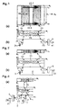
- Figure 5 shows a first embodiment of an IO sensor used in the invention in a top view ( Fig. 5(a) ) and a side view (Fig. 5(b)) .
- the sensor is provided with two chirped gratings 1.1, 1.2 as in the arrangement of Fig. 4.
- the width (in y direction) of the sensor is strongly reduced compared with that of Fig. 4.
- the size of the entire sensing unit (i.e., the pair of grating pads1.1, 1.2) in the y-direction is preferably smaller than 5 times the width of the guided mode 22 or smaller than 1 mm. With such a small lateral dimension, the dynamic range of a conventional sensor according to Fig. 4 would be unacceptably low.
- the senor used in the invention actively clamps or stabilizes the lateral position y b of the guided mode 22 to be constant by means of an additional degree of freedom.
- the additional degree of freedom may be, e.g., the wavelength of light ⁇ ; other possible degrees of freedom are the angle of incidence ⁇ i or the spectral light distribution.
- a feedback is provided from the detector 4 to the light source 3, thus establishing a controlled closed-loop system.
- the drawbacks discussed with reference to Fig. 4 are eliminated by changing the wavelength ⁇ of the light source 3 in order to keep the IOLP position y b fixed at all times.
- a substantial reduction in sensor size is achieved by compensating the effect of the measurand M.
- the dynamic range of this sensor is no longer determined by the physical size of the sensing unit, but by the range ⁇ in which the wavelength ⁇ can be varied, and of the chirp of the grating coupler 1.1. Inhomogeneities of the sensor are of minor importance because the sensor width and area are extremely small.
- Typical thicknesses of waveguiding films WG are in the range between 100 nm and 300 nm, e.g., 150 nm.
- the light source 3 is typically narrow-band light source such as a laser emitting a wavelength of, e.g., 632.8 nm, 650 nm, 785.1 nm or 980 nm.
- Typical grating periods A are in the range between 250 nm and 500 nm.
- Singly periodic, multiply periodic and/or superposed gratings 1.1, 1.2 may be used.
- a plurality of wavelengths, incoupling angles and/or polarizations may be present at the same time.
- the wavelengths, incoupling angles and/or polarizations may be discrete or exhibit a broad-band distribution.
- a further reduction of the sensor dimensions can be achieved with the sensor shown in Figure 6 (top view, Fig. 6(a), side view, Fig. 6(b) ), which is a further development of the embodiment of Fig. 5.
- the sensor dimensions are reduced also in the z direction by means of introducing yet another degree of freedom, for example by using a single grating coupler 1 working at two (or more) different diffraction orders.
- Yet another degree of freedom could by introduced by observing scattered light emitted from the grating structure (cf. Fig. 7)
- > 2 can also be used for in- or outcoupling.
- Figure 7 shows a further embodiment of an IO sensor used in the invention.
- the intensity distribution of light 25 scattered in the region of the resonant waveguide grating structure 1 is measured.
- a measurement can be performed by imaging at least a part of the resonant waveguide grating structure 1 onto a light intensity detector 4, e.g., a photodiode, by means of an imaging system 6.
- the sensor could alternatively dispense with the imaging system 6 if the light detector 4 was placed near the resonant waveguide grating structure 1 (cf. Fig. 11(a)).
- the scattered light 25 could also be guided to a detector by an optical fiber.
- Light scattering may have "natural” causes such as imperfections in the resonant waveguide grating structure 1, or “artificial” causes such as roughening of the waveguide surface or implanted imperfections in the waveguide WG.
- the intensity of the scattered light 25 is a measure for the photon density in the region of the resonant waveguide grating structure 1, which is high if a resonant electromagnetic field 22 is excited by the incident light 21 and low otherwise.
- the embodiment of Fig. 7 is an example of resonant incoupling and non-resonant outcoupling.
- a feedback loop (here not shown) for controlling a parameter of the incident light, e.g., its wavelength, could be provided as in Figs. 5 and 6.
- Figure 8 shows a side view of an embodiment of a multiple arrangement of IO sensors used in the invention.
- a plurality of IO sensors S1-S4 are arranged in e.g., an array in a surface plane 10 on a transparent substrate S.
- the details of the resonant waveguide grating structures 1.1-1.4 can be similar as those in Figs. 5-7 and are not shown in Fig. 8.
- filter structures as described in D. Shin, S. Tibuleac, Th. A Maldonado and R. Magnusson, "Thin-film optical filters with diffractive elements and waveguides", Opt, Eng. 37(9), 2634-2646 (September 1998) can be used.
- the IO sensors S1-S4 of this multiple arrangement are operated by resonant incoupling and non-resonant outcoupling, as the sensor shown in Fig. 7.
- the angle of incidence is preferably chosen to be the Brewster angle ⁇ B ; then, if the incoming light is p polarized, undesirable reflected light is reduced almost to zero.
- n WG 2.350
- n SL 1.405
- n C 1.328
- the surface plane 10 containing the resonant waveguide grating structures 1.1-1.4 is imaged onto a surface plane 40 containing a plurality of light intensity detectors 4.1-4.4 by an imaging system 6.
- the intensity of light 25 scattered in the region of the resonant waveguide grating structures 1.1-1.4 is measured by the light detectors4.1-4.4.
- each detector 4.1-4.4 is biuniquely assigned to a certain resonant waveguide grating structure 1.1-1.4.
- a parameter of the incident light 21, preferably the wavelength ⁇ 1 is varied with time in order to excite resonant electromagnetic fields in the resonant waveguide grating structures 1.1-1.4.
- the arrangement of Fig. 8 can also be operated by imaging resonantly outcoupled light in a chosen diffraction order onto the detector.
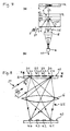
- Figure 9 shows a preferred embodiment of a multiple arrangement of IO sensors S1, S2, ... used in the invention in a top view ( Fig. 9(a) ) and a side view ( Fig. 9(b) ).
- the sensors S1, S2, ... are arranged in a two-dimensional array on a substrate S, e.g., in equally spaced rows and columns.
- the sensors S1, S2, ... can be used for obtaining a measuring signal or a referencing signal (cf. Fig. 1), i.e., some of them could also be referenced as R.
- They are illuminated preferably by a single incident light beam 21 with a defined wavelength ⁇ 1 under a defined angle of incidence ⁇ 1 .
- the incident light 21 could provide a wide range of wavelengths, different polarizations and/or a wide range of angles of incidence, or could contain a plurality of discrete wavelengths and/or of discrete angles of incidence.
- a parameter or several parameters of the incident light 21 such as the wavelength ⁇ 1 , the angle of incidence ⁇ 1 , the polarization and/or the wavefront is varied during the measurement. If the resonance conditions are fulfilled, the incident light 21 excites a resonant electromagnetic field in at least one resonant waveguide grating structure 1.1, 1.2, ... As a measure for resonance, e.g., the light distribution of resonantly outcoupled light 23 is detected for each resonant waveguide grating structure 1.1, 1.2, ... by light position detectors 4.1, 4.2, ..., e.g., CCD arrays.
- an imaging system 6 can be arranged between the resonant waveguide grating structures 1.1, 1.2, ... and the position detectors 4.1, 4.2, ...
- each position detector 4.1, 4.2, ... is biuniquely assigned to a certain resonant waveguide grating structure 1.1, 1.2, ...
- a cylindrical focusing optical system (not shown) can be used, the position detectors 4.1, 4.2, ... lying in the focal plane 40 of the cylindrical optical system.
- the cylindrical optical system acts as means for the variation of the angle of excidence into a variation of light position on the detectors 4.1, 4.2, ...; in other words, it performs an optical Fourier transform of the outcoupled light 23.
- FIG 10 various means for varying the angle of incidence ⁇ 1 are shown.
- Light 21 is emitted by a point light source 3, e.g., a vertical cavity surface emitting laser (VCSEL), a distributed feedback (DFB) laser or a distributed Bragg reflector (DBR) laser, which lies in a focal plane 30 of a collimating optical system 31.
- a point light source 3 e.g., a vertical cavity surface emitting laser (VCSEL), a distributed feedback (DFB) laser or a distributed Bragg reflector (DBR) laser, which lies in a focal plane 30 of a collimating optical system 31.
- the position of the optical system 31 is varied from a first position (full lines) to a second position (dashed lines), thus varying the angle of incidence from ⁇ 1 to ⁇ 2 .
- the position of the point light source 3 is varied.
- the embodiment of Figure 10(c) does not require any moving parts.
- a plurality of point light sources 3.1-3.5 arranged in the focal plane 30 of a collimating optical system 31 is provided.
- the angle of incidence ⁇ 1 is discretely varied by switching on different light sources 3.1-3.5.
- a further possibility for variation is the use of a mirror 32 rotatable around a rotation axis a as shown in Figure 10(d) .
- the variation of the angle of incidence can be used for exciting a resonant electromagnetic field in a resonant waveguide grating structure, but also in order to compensate for chip tolerances and/or to achieve a wider dynamic range.
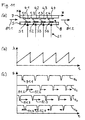
- FIG. 11(a) A further embodiment of a multiple arrangement of IO sensors S1, S2, ... used in the invention is shown in Figure 11(a) in a side view.
- the resonant waveguide grating structures 1.1, 1.2, ... can, e.g., be arranged in a two-dimensional array on a first substrate S as in Fig. 9.
- Various resonant waveguide grating structures 1.1, 1.2, ... as discussed with reference to the previous figures can be used.
- Other angles of incidence as shown in the previous figures, e.g., the Brewster angle (cf. Fig. 8), are also possible.
- an array of light intensity detectors 4.1, 4.2, ..., e.g., a photodiode array, on a second substrate D is positioned close to the resonant waveguide grating structures 1.1, 1.2, ...
- the light detectors 4.1, 4.2, ... measure, e.g., the intensity of transmitted light (not shown) for the corresponding resonant waveguide grating structures 1.1, 1.2, ...
- the embodiment of Fig. 11(a) presents the following differences: the transmitted light is measured instead of reflected light, and it is detected directly without an imaging system.
- the gap 8 between the first substrate S and the second substrate D can be used as a channel for an analyte, the flow of which is symbolized by arrows 81.1, 81.2.
- the resonant electromagnetic fields in the resonant waveguide grating structures are excited by varying a parameter of the incident light, e.g., its wavelength ⁇ .
- Figure 11(b) shows a periodic variation of the wavelength ⁇
- Figure 11(c) shows possible corresponding sensor output signals s 1 , s 2 , ... versus time t.
- Minimums or dips 91.1, 91.2, ... of the output signals s 1 , s 2 , ... are periodically detected at different times, i.e., at different wavelengths, if the sensors S1, S2, ... and/or their environments are not exactly identical.
- This arrangement is particularly fitted for measuring changes in refractive index absorption or scattering properties, or any combination thereof.
- the achievable precision (sensitivity, resolution) of the sensing process depends critically on the proper evaluation (e.g. determination of the positions of the dips in the arrangements according to Fig. 11, or of corresponding intensity peaks which will typically be observed in the arrangements of Figs. 7, 8, 9 working in the domain of reflection).
- FIG. 12 shows various embodiments of resonant waveguide grating structures 1.3-1.6 for an IO sensor according to the invention ( Figures 12(a), (c), (e) and (g) ), and their electromagnetic field intensities I versus the y coordinate ( Figures 12(b), (d), (f) and (h) ).
- the intensity I(y) of an electromagnetic field resonantly excited via a chirped grating 1.3 exhibits a sharp peak 93 at a certain position y b1 ( Figure 12(b) ; cf. Figure 5(a)).
- the intensity signal of Fig. 12(b) can be fitted (using, e.g., a Gaussian intensity distribution model).
- the peak 93 moves from its original position y b1 (full line) towards a different position y b2 (dashed line) if a parameter of the waveguide or of the incident light such as the wavelength is changed.
- the peak 93 can be clamped or stabilized at a certain y position by providing a controlled closed-loop system.
- the discrete grating 1.4 of Figure 12(c) is obtained by dividing the chirped grating 1.3 of Fig. 12(a) into a plurality of regions 1.41-1.44, i.e., stripes in y direction, and providing in each region 1.41-1.44 a homogeneous grating with a grating period which is equal to an average grating period of the corresponding region in the chirped grating 1.3.
- the intensity distribution I(y) generally exhibits different levels for the different regions 1.41-1.44; the levels change with varying light parameters or waveguide parameters ( Figure 12(d) ).
- the value of a measurand M can be evaluated by interpolating between two intensity distributions for known measurands M 1 , M 2 .
- the intensity levels can also be clamped or stabilized to be constant by providing a controlled closed-loop system 5.
- the discrete gratings need not be adjacent to each other, and their grating periods need not increase monotonously with the y coordinate, as is the case for the resonant waveguide grating structure 1.5 of Figure 12(e) ; a possible corresponding intensity distribution I(y) is shown in Figure 12(f) .
- the embodiment of Figure 12(g) has a non-periodic resonant waveguide grating structure 1.6. It exhibits a generally irregular intensity distribution I(y) such as sketched in Figure 12(h) .
- Fig. 12(g) has the advantages that imperfections of the resonant waveguide grating structure 1.6 do not disturb the measurements, and that a mathematical fit of a measured intensity distribution I(y) need not be performed.
- a method for the signal evaluation shall be presented.
- the output signals s 1 and s 2 are known for known measurand values M 1 and M 2 , respectively.
- the embodiment of Figure 13 shown in a top view applies the principle of Figs. 12(g) and (h) to a multiple arrangement of IO sensors.
- the resonant waveguide grating structures 1.1, 1.2, ... need not be in rows or columns.
- the resonant waveguide grating structure 1.3 is an example of two superposed gratings.
Landscapes
- Physics & Mathematics (AREA)
- Chemical & Material Sciences (AREA)
- Engineering & Computer Science (AREA)
- Chemical Kinetics & Catalysis (AREA)
- Plasma & Fusion (AREA)
- Health & Medical Sciences (AREA)
- Life Sciences & Earth Sciences (AREA)
- Analytical Chemistry (AREA)
- Biochemistry (AREA)
- General Health & Medical Sciences (AREA)
- General Physics & Mathematics (AREA)
- Immunology (AREA)
- Pathology (AREA)
- Investigating Or Analysing Materials By Optical Means (AREA)
Claims (20)
- Capteur opto-chimique et/ou opto-biochimique comprenant:une structure de grille de guide d'ondes résonante en optique intégrée (1, 1.1, 1.2, ...) définissant une surface plane (10);des moyens pour émettre un rayonnement électromagnétique (21) vers la structure de grille de guide d'ondes résonante (1, 1.1, 1.2, ...);
la disposition mutuelle de la structure de grille de guide d'ondes résonante (1, 1.1, 1.2, ...) et les moyens (3) pour émettre un rayonnement électromagnétique (21) étant tels que les angles d'incidence (θi) par rapport à une ligne normale sur cette surface plane (10) sont plus grands que - 90° et plus petits que + 90°, etdes moyens détecteurs (4, 4.1, 4.2, ...) pour détecter le rayonnement électromagnétique (23, 25) qui sort de la structure de grille de guide d'ondes résonante (1, 1.1, 1.2, ...);caractérisé en ce que
la disposition mutuelle de la structure de grille de guide d'ondes résonante (1, 1.1, 1.2, ...) et les moyens détecteurs (4, 4.1, 4.2, ...) étant tels que les angles, par lesquels le rayonnement électromagnétique détecté par les moyens détecteurs (4, 4.1, 4.2, ...) sort, par rapport à une ligne normale sur cette surface plane (10), sont plus grands que - 90° et plus petits que + 90° et diffèrent des angles d'incidence (θi),
les moyens (3) pour émettre un rayonnement électromagnétique (21) comprennent des moyens (3, 31, 32) pour varier périodiquement la longueur d'onde (λ) du rayonnement électromagnétique (21) émis. - Capteur selon la revendication 1, dans lequel lesdits moyens (3) pour émettre un rayonnement électromagnétique (21) comprennent une source de lumière à bande étroite accordable telle qu'un laser à cavité verticale à émission par la surface (VCSEL), un laser à rétroaction distribuée (DFB) et/ou un laser à réflecteur de Bragg distribué (DBR).
- Capteur selon la revendication 1 ou 2, dans lequel lesdits moyens (3) pour émettre un rayonnement électromagnétique (21) comprennent des moyens pour émettre une pluralité de longueurs d'onde, de préférence discrètes, d'angles d'incidence et/ou de polarisations.
- Capteur selon l'une des revendications 1 à 3, dans lequel ladite structure de grille de guide d'ondes résonante (1, 1.1, 1.2, ...) comprend au moins un réseau à périodicité unique, à périodicité multiple et/ou à fréquence pulsée, et/ou plusieurs réseaux superposés.
- Capteur selon l'une des revendications 1 à 4, dans lequel lesdits moyens détecteurs (4, 4.1, 4.2, ...) comprennent un seul détecteur ou un ensemble unidimensionnel ou bidimensionnel de détecteurs, de préférence un dispositif détecteur à couplage de charges (CCD).
- Capteur selon l'une des revendications 1 à 5, comprenant des moyens (6) pour imager ladite structure de grille de guide d'ondes résonante (1, 1.1, 1.2, ...) sur lesdits moyens détecteurs (4, 4.1, ...), ou des moyens pour transformer une variation de l'angle (θo) par lequel le rayonnement électromagnétique sort, en une variation de la position de la lumière sur lesdits moyens détecteurs (4, 4.1, 4.2, ...).
- Capteur selon l'une des revendications 1 à 6, comprenant des moyens (5) pour fournir une rétroaction à partir desdits moyens détecteurs (4) vers lesdits moyens (3) pour émettre un rayonnement électromagnétique (21), établissant de la sorte un système commandé en circuit fermé.
- Capteur selon l'une des revendications 1 à 7, dans lequel ladite structure de grille de guide d'ondes résonante (1, 1.1, 1.2, ...) est enduite avec une couche de capteur (SL) appropriée pour une réaction chimique avec une substance à capter.
- Disposition unidimensionnelle, bidimensionnelle ou tridimensionnelle multiple d'une pluralité de capteurs (S1, S2, ...) comme définis dans l'une des revendications 1 à 8.
- Disposition unidimensionnelle, bidimensionnelle multiple de capteurs (S1, S2, ...) selon la revendication 9, dans laquelle les structures de grille de guide d'ondes résonante (1, 1.1, 1.2, ...) sont agencées dans une seule surface plane (10).
- Disposition multiple de capteurs (S1, S2, ...) selon la revendication 9 ou 10, dans laquelle au moins un capteur de mesure (S) est fournit pour capter une substance chimique et/ou biochimique et au moins un capteur de référence (R) est fournit pour déduire un signal de référence.
- Disposition multiple de capteurs (S1, S2, ...) selon la revendication 13, dans laquelle chaque capteur de mesure (S) est adjacent à au moins deux et de préférence quatre capteurs de référence (R).
- Méthode pour capter optiquement une substance chimique et/ou biochimique, comprenant les étapes de:fournir une structure de grille de guide d'ondes résonante en optique intégrée (1, 1.1, 1.2, ...) définissant une surface plane (10);porter la substance en contact avec la structure de grille de guide d'ondes résonante (1, 1.1, 1.2, ...);émettre un rayonnement électromagnétique (21) vers la structure de grille de guide d'ondes résonante (1, 1.1, 1.2, ...), les angles d'incidence (θi) par rapport à une ligne normale sur ladite surface plane (10) étant plus grands que - 90° et plus petits que + 90°;exciter un champ électromagnétique résonant (22) dans la structure de grille de guide d'ondes résonante (1, 1.1, 1.2, ...), à l'aide du rayonnement électromagnétique (21) émis;provoquer une interaction de la substance avec le champ électromagnétique résonant (22); etdétecter le rayonnement électromagnétique qui sort de la structure de grille de guide d'ondes résonante (1, 1.1, 1.2, ...), les angles, par lesquels le rayonnement électromagnétique détecté sort, par rapport à une ligne normale sur ladite surface plane (10), étant plus grands que - 90° et plus petits que + 90°;caractérisée en ce que
la longueur d'onde (λ) du rayonnement électromagnétique (21) émis est périodiquement variée. - Méthode selon la revendication 13, dans laquelle le rayonnement électromagnétique (21) émis est entre une ou plusieurs bandes spectrales étroites, ou comporte une pluralité de longueurs d'onde, de préférence discrètes, d'angles d'incidence et/ou de polarisations.
- Méthode selon la revendication 13 ou 14, dans laquelle le champ électromagnétique résonant (22) est excité en utilisant un premier ordre de diffraction et le rayonnement électromagnétique (23) sortant est couplé à la sortie à travers un deuxième ordre de diffraction différent.
- Méthode selon l'une des revendications 13 à 15, dans laquelle la position d'une partie au moins du rayonnement électromagnétique (23) émergent est détectée, ou l'intensité d'une partie au moins du rayonnement électromagnétique (25) émergent est détectée.
- Méthode selon l'une des revendications 13 à 16, dans laquelle une variation de l'angle (θo) avec lequel le rayonnement électromagnétique sort est transformé en une variation d'une position de lumière, ou ladite structure de grille de guide d'ondes résonante (1, 1.1, 1.2, ...) est imagée sur un plan image (40).
- Méthode selon l'une des revendications 13 à 17, dans laquelle au moins un paramètre du rayonnement électromagnétique (21) émis est commandé par au moins un paramètre du rayonnement électromagnétique (23, 25) détecté.
- Méthode selon la revendication 18, dans laquelle le rayonnement sortant (23, 25) de la structure de grille de guide d'ondes résonante est stabilisé pour être constant en commandant au moins un paramètre du rayonnement électromagnétique (21) émis.
- Méthode selon l'une des revendications 13 à 19, dans laquelle la corrélation mathématique d'au moins deux signaux (s, s1), détectés à des moments différents (t) et/ou à des endroits différents (y), est utilisée pour déduire un signal de sortie.
Priority Applications (3)
| Application Number | Priority Date | Filing Date | Title |
|---|---|---|---|
| DE69933193T DE69933193T2 (de) | 1999-02-25 | 1999-02-25 | Integrierter optischer Sensor und Verfahren zum integrierten optischen Nachweis einer Substanz |
| EP99103730A EP1031828B1 (fr) | 1999-02-25 | 1999-02-25 | Capteur en optique intégrée et méthode pour déterminer en optique intégrée une substance |
| US09/510,609 US6429022B1 (en) | 1999-02-25 | 2000-02-22 | Integrated-optical sensor and method for integrated-optically sensing a substance |
Applications Claiming Priority (1)
| Application Number | Priority Date | Filing Date | Title |
|---|---|---|---|
| EP99103730A EP1031828B1 (fr) | 1999-02-25 | 1999-02-25 | Capteur en optique intégrée et méthode pour déterminer en optique intégrée une substance |
Publications (2)
| Publication Number | Publication Date |
|---|---|
| EP1031828A1 EP1031828A1 (fr) | 2000-08-30 |
| EP1031828B1 true EP1031828B1 (fr) | 2006-09-13 |
Family
ID=8237645
Family Applications (1)
| Application Number | Title | Priority Date | Filing Date |
|---|---|---|---|
| EP99103730A Expired - Lifetime EP1031828B1 (fr) | 1999-02-25 | 1999-02-25 | Capteur en optique intégrée et méthode pour déterminer en optique intégrée une substance |
Country Status (3)
| Country | Link |
|---|---|
| US (1) | US6429022B1 (fr) |
| EP (1) | EP1031828B1 (fr) |
| DE (1) | DE69933193T2 (fr) |
Cited By (10)
| Publication number | Priority date | Publication date | Assignee | Title |
|---|---|---|---|---|
| US7875434B2 (en) | 2000-10-30 | 2011-01-25 | Sru Biosystems, Inc. | Label-free methods for performing assays using a colorimetric resonant reflectance optical biosensor |
| US7923239B2 (en) | 2000-10-30 | 2011-04-12 | Sru Biosystems, Inc. | Guided mode resonant filter biosensor using a linear grating surface structure |
| US7927822B2 (en) | 2002-09-09 | 2011-04-19 | Sru Biosystems, Inc. | Methods for screening cells and antibodies |
| US7927789B1 (en) | 2002-12-04 | 2011-04-19 | Sru Biosystems, Inc. | Self-referencing biodetection method and patterned bioassays |
| US7935520B2 (en) | 2000-10-30 | 2011-05-03 | Sru Biosystems, Inc. | Optical detection of label-free biomolecular interactions using microreplicated plastic sensor elements |
| US8101423B2 (en) | 2000-10-30 | 2012-01-24 | Sru Biosystems, Inc. | Label-free high-throughput optical technique for detecting biomolecular interactions |
| US8257936B2 (en) | 2008-04-09 | 2012-09-04 | X-Body Inc. | High resolution label free analysis of cellular properties |
| US8298780B2 (en) | 2003-09-22 | 2012-10-30 | X-Body, Inc. | Methods of detection of changes in cells |
| US8514391B2 (en) | 1999-11-05 | 2013-08-20 | Board Of Regents, The University Of Texas System | Resonant waveguide-grating devices and methods for using same |
| US9134307B2 (en) | 2007-07-11 | 2015-09-15 | X-Body, Inc. | Method for determining ion channel modulating properties of a test reagent |
Families Citing this family (92)
| Publication number | Priority date | Publication date | Assignee | Title |
|---|---|---|---|---|
| US8111401B2 (en) | 1999-11-05 | 2012-02-07 | Robert Magnusson | Guided-mode resonance sensors employing angular, spectral, modal, and polarization diversity for high-precision sensing in compact formats |
| US6785433B2 (en) * | 2000-08-09 | 2004-08-31 | Artificial Sensing Instruments Asi Ag | Waveguide grid array and optical measurement arrangement |
| DE10043113C2 (de) * | 2000-08-31 | 2002-12-19 | Pe Diagnostik Gmbh | Verfahren zur Verbesserung der Messgenauigkeit bei Sensoren, insbesondere Bio-Sensoren, die Fluoreszenzstrahlung auswerten |
| US6951715B2 (en) * | 2000-10-30 | 2005-10-04 | Sru Biosystems, Inc. | Optical detection of label-free biomolecular interactions using microreplicated plastic sensor elements |
| US7524625B2 (en) | 2000-10-30 | 2009-04-28 | Sru Biosystems, Inc. | Real time binding analysis of antigens on a biosensor surface |
| DE20104445U1 (de) | 2001-03-13 | 2001-06-21 | pe Diagnostik GmbH, 04416 Markkleeberg | Fluoreszenzstandard |
| DE20104446U1 (de) | 2001-03-13 | 2001-06-21 | pe Diagnostik GmbH, 04416 Markkleeberg | Fluoreszenzstandard |
| WO2002084264A1 (fr) * | 2001-04-11 | 2002-10-24 | Thermo Fast U.K. Limited | Procede de mesure faisant appel a un biodetecteur optique resonant |
| CA2460233A1 (fr) | 2001-09-13 | 2003-03-20 | Axela Biosensors Inc. | Methode et appareil d'analyse reposant sur la diffraction de lumiere |
| DE10163657B4 (de) * | 2001-12-21 | 2008-05-08 | Gedig, Erk, Dr. | Vorrichtung und Verfahren zur Untersuchung dünner Schichten |
| US7872804B2 (en) | 2002-08-20 | 2011-01-18 | Illumina, Inc. | Encoded particle having a grating with variations in the refractive index |
| US7441703B2 (en) | 2002-08-20 | 2008-10-28 | Illumina, Inc. | Optical reader for diffraction grating-based encoded optical identification elements |
| US7164533B2 (en) | 2003-01-22 | 2007-01-16 | Cyvera Corporation | Hybrid random bead/chip based microarray |
| US7901630B2 (en) | 2002-08-20 | 2011-03-08 | Illumina, Inc. | Diffraction grating-based encoded microparticle assay stick |
| US7508608B2 (en) | 2004-11-17 | 2009-03-24 | Illumina, Inc. | Lithographically fabricated holographic optical identification element |
| US7923260B2 (en) | 2002-08-20 | 2011-04-12 | Illumina, Inc. | Method of reading encoded particles |
| US7900836B2 (en) | 2002-08-20 | 2011-03-08 | Illumina, Inc. | Optical reader system for substrates having an optically readable code |
| US7092160B2 (en) | 2002-09-12 | 2006-08-15 | Illumina, Inc. | Method of manufacturing of diffraction grating-based optical identification element |
| CA2498933C (fr) | 2002-09-12 | 2012-08-28 | Cyvera Corporation | Procede et appareil d'alignement de microbilles allongees de maniere a les interroger |
| AU2003270726A1 (en) | 2002-09-12 | 2004-04-30 | Cidra Corporation | Diffraction grating-based encoded micro-particles for multiplexed experiments |
| US20100255603A9 (en) | 2002-09-12 | 2010-10-07 | Putnam Martin A | Method and apparatus for aligning microbeads in order to interrogate the same |
| US6810067B2 (en) * | 2002-09-26 | 2004-10-26 | Photodigm, Inc. | Single mode grating-outcoupled surface emitting laser with broadband and narrow-band DBR reflectors |
| US7027163B2 (en) * | 2003-01-24 | 2006-04-11 | General Dynamics Advanced Information Systems, Inc. | Grating sensor |
| WO2004092730A2 (fr) * | 2003-04-15 | 2004-10-28 | Biogenon Ltd. | Methode et dispositif de detection de la presence d'un analyte |
| US20040241659A1 (en) * | 2003-05-30 | 2004-12-02 | Applera Corporation | Apparatus and method for hybridization and SPR detection |
| US7057720B2 (en) * | 2003-06-24 | 2006-06-06 | Corning Incorporated | Optical interrogation system and method for using same |
| US7292333B2 (en) * | 2003-06-24 | 2007-11-06 | Corning Incorporated | Optical interrogation system and method for 2-D sensor arrays |
| US6985664B2 (en) * | 2003-08-01 | 2006-01-10 | Corning Incorporated | Substrate index modification for increasing the sensitivity of grating-coupled waveguides |
| CN100559182C (zh) * | 2003-08-29 | 2009-11-11 | 株式会社东芝 | 显色试剂、浓度测定试剂盒、浓度测定方法和在该方法中使用的传感器芯片 |
| US7433123B2 (en) | 2004-02-19 | 2008-10-07 | Illumina, Inc. | Optical identification element having non-waveguide photosensitive substrate with diffraction grating therein |
| DE102004009543B4 (de) * | 2004-02-23 | 2006-09-28 | Siemens Ag | Leuchtplatte zur Evaneszenzfeldanregung und Verfahren zu deren Verwendung |
| US7042342B2 (en) * | 2004-06-09 | 2006-05-09 | Lear Corporation | Remote keyless entry transmitter fob with RF analyzer |
| FR2871571B1 (fr) * | 2004-06-11 | 2007-03-16 | Cybernetix Sa | Procede de detecton et detecteur optique de gaz |
| WO2006020363A2 (fr) | 2004-07-21 | 2006-02-23 | Illumina, Inc. | Procede et dispositif de suivi de produits medicamenteux au moyen d'elements d'identification optique codes |
| US7522786B2 (en) * | 2005-12-22 | 2009-04-21 | Palo Alto Research Center Incorporated | Transmitting light with photon energy information |
| US7604173B2 (en) | 2004-11-16 | 2009-10-20 | Illumina, Inc. | Holographically encoded elements for microarray and other tagging labeling applications, and method and apparatus for making and reading the same |
| US7602952B2 (en) | 2004-11-16 | 2009-10-13 | Illumina, Inc. | Scanner having spatial light modulator |
| ATE459933T1 (de) | 2004-11-16 | 2010-03-15 | Illumina Inc | Verfahren und vorrichtung zum lesen von kodierten mikrokugeln |
| US7403284B2 (en) * | 2004-12-16 | 2008-07-22 | Andevices, Inc. | Integrated optics based high-resolution spectrophotometer |
| WO2006108183A2 (fr) * | 2005-04-05 | 2006-10-12 | Corning Incorporated | Biocapteurs et cellules sans etiquette |
| CN1940529B (zh) * | 2005-09-29 | 2010-09-01 | 株式会社东芝 | 光波导型生物化学传感器芯片及其制造方法 |
| US7623624B2 (en) | 2005-11-22 | 2009-11-24 | Illumina, Inc. | Method and apparatus for labeling using optical identification elements characterized by X-ray diffraction |
| US7218802B1 (en) | 2005-11-30 | 2007-05-15 | Corning Incorporated | Low drift planar waveguide grating sensor and method for manufacturing same |
| US7433552B2 (en) * | 2005-12-22 | 2008-10-07 | Palo Alto Research Center Incorporated | Obtaining analyte information |
| US8437582B2 (en) | 2005-12-22 | 2013-05-07 | Palo Alto Research Center Incorporated | Transmitting light with lateral variation |
| US7547904B2 (en) * | 2005-12-22 | 2009-06-16 | Palo Alto Research Center Incorporated | Sensing photon energies emanating from channels or moving objects |
| US7315667B2 (en) * | 2005-12-22 | 2008-01-01 | Palo Alto Research Center Incorporated | Propagating light to be sensed |
| US7358476B2 (en) * | 2005-12-22 | 2008-04-15 | Palo Alto Research Center Incorporated | Sensing photons from objects in channels |
| US7386199B2 (en) * | 2005-12-22 | 2008-06-10 | Palo Alto Research Center Incorporated | Providing light to channels or portions |
| US7420677B2 (en) * | 2005-12-22 | 2008-09-02 | Palo Alto Research Center Incorporated | Sensing photon energies of optical signals |
| US7830575B2 (en) | 2006-04-10 | 2010-11-09 | Illumina, Inc. | Optical scanner with improved scan time |
| JP2009543055A (ja) * | 2006-06-30 | 2009-12-03 | コーニング インコーポレイテッド | フロースルーアッセイ用の流体取扱システム |
| WO2008010182A2 (fr) * | 2006-07-17 | 2008-01-24 | Max Wiki | Système analytique présentant un dispositif de modulation de la lumière dans l'espace et variant en fonction du temps, et procédé d'identification mis en oeuvre au moyen de ce système |
| US7652767B2 (en) * | 2006-10-19 | 2010-01-26 | Sporian Microsystems, Inc. | Optical sensor with chemically reactive surface |
| US7602496B2 (en) * | 2006-10-19 | 2009-10-13 | Sporian Microsystems, Inc. | Optical sensor with biologically reactive surface |
| US9164037B2 (en) | 2007-01-26 | 2015-10-20 | Palo Alto Research Center Incorporated | Method and system for evaluation of signals received from spatially modulated excitation and emission to accurately determine particle positions and distances |
| US8821799B2 (en) | 2007-01-26 | 2014-09-02 | Palo Alto Research Center Incorporated | Method and system implementing spatially modulated excitation or emission for particle characterization with enhanced sensitivity |
| US7545513B2 (en) * | 2007-02-05 | 2009-06-09 | Palo Alto Research Center Incorporated | Encoding optical cavity output light |
| US7936463B2 (en) * | 2007-02-05 | 2011-05-03 | Palo Alto Research Center Incorporated | Containing analyte in optical cavity structures |
| US7502123B2 (en) * | 2007-02-05 | 2009-03-10 | Palo Alto Research Center Incorporated | Obtaining information from optical cavity output light |
| US7852490B2 (en) * | 2007-02-05 | 2010-12-14 | Palo Alto Research Center Incorporated | Implanting optical cavity structures |
| US7633629B2 (en) * | 2007-02-05 | 2009-12-15 | Palo Alto Research Center Incorporated | Tuning optical cavities |
| US7554673B2 (en) * | 2007-02-05 | 2009-06-30 | Palo Alto Research Center Incorporated | Obtaining information about analytes using optical cavity output light |
| US7817276B2 (en) | 2007-02-05 | 2010-10-19 | Palo Alto Research Center Incorporated | Distinguishing objects |
| US7599055B2 (en) * | 2007-02-27 | 2009-10-06 | Corning Incorporated | Swept wavelength imaging optical interrogation system and method for using same |
| DK2137514T3 (en) | 2007-03-13 | 2018-10-01 | Creoptix Ag | Integrated optical sensor. |
| US11064236B2 (en) * | 2007-05-11 | 2021-07-13 | Verizon Patent And Licensing Inc. | Systems and methods for using value-added services records to provide targeted marketing services |
| CN101802611A (zh) | 2007-07-11 | 2010-08-11 | Sru生物系统公司 | 鉴别离子通道调节剂的方法 |
| US8320983B2 (en) * | 2007-12-17 | 2012-11-27 | Palo Alto Research Center Incorporated | Controlling transfer of objects affecting optical characteristics |
| US8153949B2 (en) * | 2008-12-18 | 2012-04-10 | Palo Alto Research Center Incorporated | Obtaining sensing results indicating time variation |
| US7894068B2 (en) * | 2008-02-04 | 2011-02-22 | Palo Alto Research Center Incorporated | Producing filters with combined transmission and/or reflection functions |
| US7763856B2 (en) * | 2008-01-31 | 2010-07-27 | Palo Alto Research Center Incorporated | Producing time variation in emanating light |
| US7701580B2 (en) * | 2008-02-01 | 2010-04-20 | Palo Alto Research Center Incorporated | Transmitting/reflecting emanating light with time variation |
| US8373860B2 (en) * | 2008-02-01 | 2013-02-12 | Palo Alto Research Center Incorporated | Transmitting/reflecting emanating light with time variation |
| US8629981B2 (en) | 2008-02-01 | 2014-01-14 | Palo Alto Research Center Incorporated | Analyzers with time variation based on color-coded spatial modulation |
| US7999944B2 (en) | 2008-10-23 | 2011-08-16 | Corning Incorporated | Multi-channel swept wavelength optical interrogation system and method for using same |
| US20100130829A1 (en) * | 2008-11-25 | 2010-05-27 | Ye Fang | Materials and methods for detecting early cell migration events |
| US8049883B2 (en) * | 2009-02-27 | 2011-11-01 | Corning Incorporated | Wavelength tracker for swept wavelength sensor interrogation system |
| US9063092B2 (en) * | 2009-09-14 | 2015-06-23 | Koninklijke Philips N.V. | Sensing system for sensing a substance in a fluid |
| US8619260B2 (en) * | 2009-11-02 | 2013-12-31 | Corning Incorporated | Multi-grating biosensor for label-independent optical readers |
| US8384905B2 (en) * | 2009-11-10 | 2013-02-26 | Corning Incorporated | Tunable light source for label-independent optical reader |
| US8723140B2 (en) | 2011-08-09 | 2014-05-13 | Palo Alto Research Center Incorporated | Particle analyzer with spatial modulation and long lifetime bioprobes |
| US9029800B2 (en) | 2011-08-09 | 2015-05-12 | Palo Alto Research Center Incorporated | Compact analyzer with spatial modulation and multiple intensity modulated excitation sources |
| US8958071B2 (en) | 2011-11-15 | 2015-02-17 | Empire Technology Development Llc | Integrated optical sensor |
| WO2013082272A1 (fr) | 2011-11-30 | 2013-06-06 | Corning Incorporated | Système à source de lumière accordable capable d'effectuer une mesure de longueur d'onde pour un système d'imagerie hyperspectrale |
| EP2824446A1 (fr) * | 2013-07-12 | 2015-01-14 | F. Hoffmann-La Roche AG | Dispositif à utiliser pour la détection des affinités de liaison |
| JP6392876B2 (ja) * | 2013-12-23 | 2018-09-19 | セエスウエム サントル スイス デレクトロニクエ ドゥ ミクロテクニク ソシエテ アノニム−ルシェルシェ エ デブロップマン | 導波モード共鳴デバイス |
| EP3205512B1 (fr) | 2016-02-09 | 2018-06-13 | CSEM Centre Suisse d'Electronique et de Microtechnique SA - Recherche et Développement | Dispositif de sécurité optique |
| GB201610647D0 (en) * | 2016-06-17 | 2016-08-03 | Univ York | Improved sensor and associated methods |
| CN111512189B (zh) | 2017-10-02 | 2023-02-21 | 瑞士Csem电子显微技术研发中心 | 谐振波导光栅及其应用 |
| TWI683085B (zh) * | 2018-10-12 | 2020-01-21 | 國立交通大學 | 光學位移感測系統 |
| CN114709714B (zh) * | 2021-08-27 | 2025-09-23 | 因林光电科技(苏州)有限公司 | 一种分布式反馈激光器及其制备方法 |
Family Cites Families (13)
| Publication number | Priority date | Publication date | Assignee | Title |
|---|---|---|---|---|
| WO1986007149A1 (fr) * | 1985-05-29 | 1986-12-04 | Kurt Tiefenthaler | Senseur optique pour etablir selectivement la presence de substances ainsi que la variation d'indice de refraction dans les substances objet de mesures |
| SE462408B (sv) * | 1988-11-10 | 1990-06-18 | Pharmacia Ab | Optiskt biosensorsystem utnyttjande ytplasmonresonans foer detektering av en specific biomolekyl, saett att kalibrera sensoranordningen samt saett att korrigera foer baslinjedrift i systemet |
| US5082629A (en) * | 1989-12-29 | 1992-01-21 | The Board Of The University Of Washington | Thin-film spectroscopic sensor |
| EP0455067B1 (fr) * | 1990-05-03 | 2003-02-26 | F. Hoffmann-La Roche Ag | Capteur microoptique |
| DE59207589D1 (de) | 1991-04-26 | 1997-01-09 | Scherrer Inst Paul | Verfahren und vorrichtung zur bestimmung einer messgrösse mittels eines integriert-optischen sensormoduls |
| GB9314991D0 (en) * | 1993-07-20 | 1993-09-01 | Sandoz Ltd | Mechanical device |
| US5737457A (en) * | 1994-02-25 | 1998-04-07 | Fci - Fiberchem, Inc. | Chip level waveguide sensor |
| CN1149335A (zh) * | 1994-05-27 | 1997-05-07 | 希巴-盖吉股份公司 | 探测短暂受激发光的方法 |
| US5577137A (en) * | 1995-02-22 | 1996-11-19 | American Research Corporation Of Virginia | Optical chemical sensor and method using same employing a multiplicity of fluorophores contained in the free volume of a polymeric optical waveguide or in pores of a ceramic waveguide |
| TW302435B (fr) | 1995-05-12 | 1997-04-11 | Ciba Geigy Ag | |
| US5623561A (en) * | 1995-09-29 | 1997-04-22 | Georgia Tech Research Corporation | Integrated optic interferometric sensor |
| GB9602542D0 (en) * | 1996-02-08 | 1996-04-10 | Fisons Plc | Analytical device |
| AU4207897A (en) * | 1996-08-29 | 1998-03-19 | Novartis Ag | Optical chemical / biochemical sensor |
-
1999
- 1999-02-25 DE DE69933193T patent/DE69933193T2/de not_active Expired - Lifetime
- 1999-02-25 EP EP99103730A patent/EP1031828B1/fr not_active Expired - Lifetime
-
2000
- 2000-02-22 US US09/510,609 patent/US6429022B1/en not_active Expired - Lifetime
Cited By (14)
| Publication number | Priority date | Publication date | Assignee | Title |
|---|---|---|---|---|
| US8514391B2 (en) | 1999-11-05 | 2013-08-20 | Board Of Regents, The University Of Texas System | Resonant waveguide-grating devices and methods for using same |
| US7923239B2 (en) | 2000-10-30 | 2011-04-12 | Sru Biosystems, Inc. | Guided mode resonant filter biosensor using a linear grating surface structure |
| US7875434B2 (en) | 2000-10-30 | 2011-01-25 | Sru Biosystems, Inc. | Label-free methods for performing assays using a colorimetric resonant reflectance optical biosensor |
| US7935520B2 (en) | 2000-10-30 | 2011-05-03 | Sru Biosystems, Inc. | Optical detection of label-free biomolecular interactions using microreplicated plastic sensor elements |
| US8101423B2 (en) | 2000-10-30 | 2012-01-24 | Sru Biosystems, Inc. | Label-free high-throughput optical technique for detecting biomolecular interactions |
| US8580578B2 (en) | 2000-10-30 | 2013-11-12 | X-Body, Inc. | Optical detection of label-free biomolecular interactions using microreplicated plastic |
| US7927822B2 (en) | 2002-09-09 | 2011-04-19 | Sru Biosystems, Inc. | Methods for screening cells and antibodies |
| US8202735B2 (en) | 2002-09-09 | 2012-06-19 | X-Body, Inc. | Methods for screening cells and antibodies |
| US8551716B2 (en) | 2002-09-09 | 2013-10-08 | X-Body, Inc. | Methods for screening cells and antibodies |
| US7927789B1 (en) | 2002-12-04 | 2011-04-19 | Sru Biosystems, Inc. | Self-referencing biodetection method and patterned bioassays |
| US8298780B2 (en) | 2003-09-22 | 2012-10-30 | X-Body, Inc. | Methods of detection of changes in cells |
| US9134307B2 (en) | 2007-07-11 | 2015-09-15 | X-Body, Inc. | Method for determining ion channel modulating properties of a test reagent |
| US8372592B2 (en) | 2008-04-09 | 2013-02-12 | X-Body, Inc. | High resolution label free analysis of cellular properties |
| US8257936B2 (en) | 2008-04-09 | 2012-09-04 | X-Body Inc. | High resolution label free analysis of cellular properties |
Also Published As
| Publication number | Publication date |
|---|---|
| EP1031828A1 (fr) | 2000-08-30 |
| DE69933193T2 (de) | 2007-08-02 |
| US6429022B1 (en) | 2002-08-06 |
| DE69933193D1 (de) | 2006-10-26 |
Similar Documents
| Publication | Publication Date | Title |
|---|---|---|
| EP1031828B1 (fr) | Capteur en optique intégrée et méthode pour déterminer en optique intégrée une substance | |
| CN102713542B (zh) | 用于非标记光阅读器的可调光源 | |
| US6819812B2 (en) | System and method for measuring physical, chemical and biological stimuli using vertical cavity surface emitting lasers with integrated tuner | |
| AU751280B2 (en) | Optical resonance analysis system | |
| EP0852715B1 (fr) | Capteur interferometrique optique integral | |
| EP1613922B1 (fr) | Procedes et systemes pour la spectroscopie multiplexe multimode statique | |
| RU2141645C1 (ru) | Способ исследования биологических, биохимических, химических характеристик сред и устройство для его осуществления | |
| JPH06300683A (ja) | 伝搬特性測定プロセス及び装置 | |
| WO1999044042A2 (fr) | Structures de guide d'onde | |
| US7239395B2 (en) | Optical interrogation systems with reduced parasitic reflections and a method for filtering parasitic reflections | |
| Piliarik et al. | SPR sensor instrumentation | |
| US20100105148A1 (en) | Multi-channel swept wavelength optical interrogation system and method for using same | |
| US20130094029A1 (en) | Vernier photonic sensor data-analysis | |
| JP2003139694A (ja) | 測定プレート | |
| US5502560A (en) | Analytical sensor using grating light reflection spectroscopy | |
| JP2005321244A (ja) | 光学的測定装置 | |
| Homola et al. | Surface plasmon resonance sensor based on planar light pipe: theoretical optimization analysis | |
| JP2004245674A (ja) | 放射温度測定装置 | |
| JP3702340B2 (ja) | 屈折率測定法 | |
| JP4067335B2 (ja) | 全反射光を利用した測定装置 | |
| JP3910498B2 (ja) | 測定装置 | |
| JP3390355B2 (ja) | 表面プラズモンセンサー | |
| Homola et al. | SPR sensor instrumentation | |
| KR20260019408A (ko) | 광학적 센싱 방법 및 광학적 센싱 방법을 위한 광학 센서 시스템 | |
| Slavik et al. | Fiber optic surface plasmon resonance sensor with a Bragg grating |
Legal Events
| Date | Code | Title | Description |
|---|---|---|---|
| PUAI | Public reference made under article 153(3) epc to a published international application that has entered the european phase |
Free format text: ORIGINAL CODE: 0009012 |
|
| AK | Designated contracting states |
Kind code of ref document: A1 Designated state(s): CH DE FR GB LI NL |
|
| AX | Request for extension of the european patent |
Free format text: AL;LT;LV;MK;RO;SI |
|
| 17P | Request for examination filed |
Effective date: 20010203 |
|
| AKX | Designation fees paid |
Free format text: CH DE FR GB LI NL |
|
| 17Q | First examination report despatched |
Effective date: 20040628 |
|
| GRAP | Despatch of communication of intention to grant a patent |
Free format text: ORIGINAL CODE: EPIDOSNIGR1 |
|
| GRAS | Grant fee paid |
Free format text: ORIGINAL CODE: EPIDOSNIGR3 |
|
| GRAA | (expected) grant |
Free format text: ORIGINAL CODE: 0009210 |
|
| AK | Designated contracting states |
Kind code of ref document: B1 Designated state(s): CH DE FR GB LI NL |
|
| PG25 | Lapsed in a contracting state [announced via postgrant information from national office to epo] |
Ref country code: NL Free format text: LAPSE BECAUSE OF FAILURE TO SUBMIT A TRANSLATION OF THE DESCRIPTION OR TO PAY THE FEE WITHIN THE PRESCRIBED TIME-LIMIT Effective date: 20060913 |
|
| REG | Reference to a national code |
Ref country code: GB Ref legal event code: FG4D |
|
| REG | Reference to a national code |
Ref country code: CH Ref legal event code: EP |
|
| REF | Corresponds to: |
Ref document number: 69933193 Country of ref document: DE Date of ref document: 20061026 Kind code of ref document: P |
|
| REG | Reference to a national code |
Ref country code: CH Ref legal event code: NV Representative=s name: SCHNEIDER FELDMANN AG PATENT- UND MARKENANWAELTE |
|
| NLV1 | Nl: lapsed or annulled due to failure to fulfill the requirements of art. 29p and 29m of the patents act | ||
| ET | Fr: translation filed | ||
| PLBE | No opposition filed within time limit |
Free format text: ORIGINAL CODE: 0009261 |
|
| STAA | Information on the status of an ep patent application or granted ep patent |
Free format text: STATUS: NO OPPOSITION FILED WITHIN TIME LIMIT |
|
| 26N | No opposition filed |
Effective date: 20070614 |
|
| REG | Reference to a national code |
Ref country code: GB Ref legal event code: S117 Free format text: REQUEST FILED; REQUEST FOR CORRECTION UNDER SECTION 117 FILED ON 12 JUNE 2009 |
|
| REG | Reference to a national code |
Ref country code: GB Ref legal event code: S117 Free format text: CORRECTIONS ALLOWED |
|
| PGFP | Annual fee paid to national office [announced via postgrant information from national office to epo] |
Ref country code: CH Payment date: 20110418 Year of fee payment: 13 |
|
| REG | Reference to a national code |
Ref country code: CH Ref legal event code: PL |
|
| PG25 | Lapsed in a contracting state [announced via postgrant information from national office to epo] |
Ref country code: LI Free format text: LAPSE BECAUSE OF NON-PAYMENT OF DUE FEES Effective date: 20120229 Ref country code: CH Free format text: LAPSE BECAUSE OF NON-PAYMENT OF DUE FEES Effective date: 20120229 |
|
| PGFP | Annual fee paid to national office [announced via postgrant information from national office to epo] |
Ref country code: FR Payment date: 20140211 Year of fee payment: 16 |
|
| PGFP | Annual fee paid to national office [announced via postgrant information from national office to epo] |
Ref country code: GB Payment date: 20140219 Year of fee payment: 16 |
|
| PGFP | Annual fee paid to national office [announced via postgrant information from national office to epo] |
Ref country code: DE Payment date: 20140417 Year of fee payment: 16 |
|
| REG | Reference to a national code |
Ref country code: DE Ref legal event code: R119 Ref document number: 69933193 Country of ref document: DE |
|
| GBPC | Gb: european patent ceased through non-payment of renewal fee |
Effective date: 20150225 |
|
| REG | Reference to a national code |
Ref country code: FR Ref legal event code: ST Effective date: 20151030 |
|
| PG25 | Lapsed in a contracting state [announced via postgrant information from national office to epo] |
Ref country code: GB Free format text: LAPSE BECAUSE OF NON-PAYMENT OF DUE FEES Effective date: 20150225 Ref country code: DE Free format text: LAPSE BECAUSE OF NON-PAYMENT OF DUE FEES Effective date: 20150901 |
|
| PG25 | Lapsed in a contracting state [announced via postgrant information from national office to epo] |
Ref country code: FR Free format text: LAPSE BECAUSE OF NON-PAYMENT OF DUE FEES Effective date: 20150302 |