EP1031882A2 - Beleuchtungssystem mit Feldspiegeln zur Erzeugung einer gleichmässigen Abtastenergie - Google Patents
Beleuchtungssystem mit Feldspiegeln zur Erzeugung einer gleichmässigen Abtastenergie Download PDFInfo
- Publication number
- EP1031882A2 EP1031882A2 EP00104014A EP00104014A EP1031882A2 EP 1031882 A2 EP1031882 A2 EP 1031882A2 EP 00104014 A EP00104014 A EP 00104014A EP 00104014 A EP00104014 A EP 00104014A EP 1031882 A2 EP1031882 A2 EP 1031882A2
- Authority
- EP
- European Patent Office
- Prior art keywords
- field
- mirror
- illumination system
- plane
- image plane
- Prior art date
- Legal status (The legal status is an assumption and is not a legal conclusion. Google has not performed a legal analysis and makes no representation as to the accuracy of the status listed.)
- Withdrawn
Links
Images




Classifications
-
- G—PHYSICS
- G03—PHOTOGRAPHY; CINEMATOGRAPHY; ANALOGOUS TECHNIQUES USING WAVES OTHER THAN OPTICAL WAVES; ELECTROGRAPHY; HOLOGRAPHY
- G03F—PHOTOMECHANICAL PRODUCTION OF TEXTURED OR PATTERNED SURFACES, e.g. FOR PRINTING, FOR PROCESSING OF SEMICONDUCTOR DEVICES; MATERIALS THEREFOR; ORIGINALS THEREFOR; APPARATUS SPECIALLY ADAPTED THEREFOR
- G03F7/00—Photomechanical, e.g. photolithographic, production of textured or patterned surfaces, e.g. printing surfaces; Materials therefor, e.g. comprising photoresists; Apparatus specially adapted therefor
- G03F7/70—Microphotolithographic exposure; Apparatus therefor
- G03F7/70058—Mask illumination systems
- G03F7/702—Reflective illumination, i.e. reflective optical elements other than folding mirrors, e.g. extreme ultraviolet [EUV] illumination systems
-
- H—ELECTRICITY
- H10—SEMICONDUCTOR DEVICES; ELECTRIC SOLID-STATE DEVICES NOT OTHERWISE PROVIDED FOR
- H10P—GENERIC PROCESSES OR APPARATUS FOR THE MANUFACTURE OR TREATMENT OF DEVICES COVERED BY CLASS H10
- H10P76/00—Manufacture or treatment of masks on semiconductor bodies, e.g. by lithography or photolithography
-
- G—PHYSICS
- G03—PHOTOGRAPHY; CINEMATOGRAPHY; ANALOGOUS TECHNIQUES USING WAVES OTHER THAN OPTICAL WAVES; ELECTROGRAPHY; HOLOGRAPHY
- G03F—PHOTOMECHANICAL PRODUCTION OF TEXTURED OR PATTERNED SURFACES, e.g. FOR PRINTING, FOR PROCESSING OF SEMICONDUCTOR DEVICES; MATERIALS THEREFOR; ORIGINALS THEREFOR; APPARATUS SPECIALLY ADAPTED THEREFOR
- G03F7/00—Photomechanical, e.g. photolithographic, production of textured or patterned surfaces, e.g. printing surfaces; Materials therefor, e.g. comprising photoresists; Apparatus specially adapted therefor
- G03F7/70—Microphotolithographic exposure; Apparatus therefor
- G03F7/70216—Mask projection systems
- G03F7/70233—Optical aspects of catoptric systems, i.e. comprising only reflective elements, e.g. extreme ultraviolet [EUV] projection systems
-
- G—PHYSICS
- G03—PHOTOGRAPHY; CINEMATOGRAPHY; ANALOGOUS TECHNIQUES USING WAVES OTHER THAN OPTICAL WAVES; ELECTROGRAPHY; HOLOGRAPHY
- G03F—PHOTOMECHANICAL PRODUCTION OF TEXTURED OR PATTERNED SURFACES, e.g. FOR PRINTING, FOR PROCESSING OF SEMICONDUCTOR DEVICES; MATERIALS THEREFOR; ORIGINALS THEREFOR; APPARATUS SPECIALLY ADAPTED THEREFOR
- G03F7/00—Photomechanical, e.g. photolithographic, production of textured or patterned surfaces, e.g. printing surfaces; Materials therefor, e.g. comprising photoresists; Apparatus specially adapted therefor
- G03F7/70—Microphotolithographic exposure; Apparatus therefor
- G03F7/70216—Mask projection systems
- G03F7/70358—Scanning exposure, i.e. relative movement of patterned beam and workpiece during imaging
-
- G—PHYSICS
- G21—NUCLEAR PHYSICS; NUCLEAR ENGINEERING
- G21K—HANDLING OF PARTICLES OR IONISING RADIATION NOT OTHERWISE PROVIDED FOR; IRRADIATION DEVICES; GAMMA RAY OR X-RAY MICROSCOPES
- G21K1/00—Arrangements for handling particles or ionising radiation, e.g. focusing or moderating
- G21K1/06—Arrangements for handling particles or ionising radiation, e.g. focusing or moderating using diffraction, refraction or reflection, e.g. monochromators
Definitions
- This invention relates to an illumination system, and more particularly to an illumination system for EUV lithography with wavelengths less than 193 nm.
- EUV illumination systems for EUV sources have been disclosed in EP 99 106 348.8 (US application serial no. 09/305017) and PCT/EP99/02999. These illumination systems are adapted to synchrotron, wiggler, undulator, Pinch-Plasma or Laser-Produced-Plasma sources.
- Scanning uniformity is a problem of the aforementioned scanning exposure systems in illuminating a slit, particularly a curved slit.
- the scanning energy obtained as a line integral over the intensity distribution along the scan path in a reticle or wafer plane may increase toward the field edge despite homogeneous illumination intensity because of the longer scan path at the field edge for a curved slit.
- scanning energy and with it scanning uniformity may also be affected by other influences, for example coating or vignetting effects are possible.
- the curved slit is typically represented by a segment of a ring field, which is also called an arc shaped field.
- the arc shaped field can be described by the width delta r, a mean Radius R 0 and the angular range 2 ⁇ 0 .
- This and other objectives of the present invention are achieved by shaping a field lens group in an illumination system of a generic type so that the illuminated field is distorted in an image plane of the illumination system perpendicular to the scanning direction. In this plane the mask or reticle of a projection exposure system is located.
- the scanning energy could be controlled by introducing x-distortion to the illuminated field using the field lens(es) or field mirror(s).
- the additional distortion acts only in the direction perpendicular to the scanning direction.
- the field lens(es) or the field mirror(s) only influences the distortion of the illuminated field, whereas other optical elements direct the light from the source to the image plane.
- the imaging is done by the pupil facet. Said imaging is influenced by the field lens(es) or the field mirror(s) according to the inventive concept.
- field lens group is taken to describe both field mirror(s) and field lens(es).
- the field lens group typically comprises refractive field lens(es), but mirrors are also possible.
- the field lens group comprises reflective field mirror(s).
- EUV lithography uses wavelengths between 10nm and 20nm, typically 13nm.
- a scanning system it is possible to determine the necessary distortion to obtain a predetermined intensity distribution. It is advantageous for a scanning system to have the capability of modifying the intensity distribution perpendicular to the scanning direction to get a uniform distribution of scanning energy in the wafer plane.
- the scanning energy can be influenced by varying the length of the scanning path or by modifying the distribution of the illumination intensity.
- the present invention relates to the correction of the distribution of the illumination intensity. In comparison to stepper systems where a two-dimensional intensity distribution has to be corrected, a scanner system only requires a correction of the distribution of the scanning energy.
- the illumination intensity decreases from the center of the field to the field edges by means of increasing distortion.
- a decrease of the illumination intensity towards the field edge permits a compensation for an increase of the scan path so that the scanning energy remains homogeneous.
- the present invention also provides for the illumination intensity to increase from the center of the field to the field edges by means of decreasing distortion. This correction can be necessary if other influences like layer or vignetting effects lead to a decreasing scanning energy towards the field edges.
- the field lens group is designed so that uniformity of scanning energy in the range of ⁇ 7%, preferably ⁇ 5%, and very preferably ⁇ 3%, is achieved in the image plane of the illumination system.
- the field lens group is shaped so, that the aperture stop plane of the illumination system is imaged into a given exit pupil of the illumination system. In addition to the intensity correction, the field lens group achieves the correct pupil imaging.
- the exit pupil of the illumination system is typically given by the entrance pupil of the projection objective.
- the location of the entrance pupil is field dependent. In such a case, the location of the exit pupil of the illumination system is also field dependent.
- the shape of the illuminated field according to this invention is rectangular or a segment of a ring field.
- the field lens group is preferably shaped such that a predetermined shaping of the illuminated field is achieved. If the illuminated field is bounded by a segment of a ring field, the design of the field lens group determines the mean radius R 0 of the ring field.
- the field mirror(s) is (are) preferably grazing incidence mirror(s).
- the illumination system includes optical components to transform the light source into secondary light sources.
- One such optical component can be a mirror that is divided into several single mirror elements. Each mirror element produces one secondary light source.
- the mirror element can be provided with a plane, spherical, cylindrical, toroidal or an aspheric surface. Theses single mirror elements are called field facets. They are imaged in an image plane of the illumination system where the images of the field facets are at least partly superimposed.
- each mirror element is located at a secondary light source.
- These mirror elements are called pupil facets.
- the pupil facets typically have a positive optical power and image the corresponding field facets into the image plane.
- the imaging of the field facets into the image plane can be divided into a radial image formation and an azimuthal image formation.
- the y-direction of a field facet is imaged in the radial direction, and the x-direction is imaged in the azimuthal direction of an arc shaped field.
- the imaging of the field facets is influenced by the field lens group. It is therefore advantageous to vary the azimuthal distortion by changing the surface parameters of the components of the field lens group.
- the field lens group is shaped such that the secondary light sources produced by the field facets are imaged into a given exit pupil of the illumination system.
- actuators on the field mirror(s) are preferably provided in order to control the reflective surface(s).
- the distortion, and thus the illumination intensity, can be modified using the actuators. Since the surface changes also affect the pupil imaging, intensity correction and pupil imaging are regarded simultaneously. The surface changes are limited by the fact that the directions of centroid rays that intersect the image plane are changed less than 5mrad, preferably less than 2mrad, and very preferably less than lmrad.
- a particularly simple arrangement is obtained when the actuators for controlling the field mirror surface are placed parallel to the scan direction or the y-axis of the field mirror, for example in the form of a line or beam actuator.
- the present invention also provides for a projection exposure system for microlithography using the previously described illumination system.
- a mask or reticle is arranged in the image plane of the illumination system, which is also an interface plane between the illumination system and projection system.
- the mask will be imaged into a wafer plane using a projection objective.
- the illumination of the wafer is typically telecentric. This means that the angles of the chief rays regarding the wafer plane are smaller than ⁇ 5mrad.
- the angle distribution of the chief rays in the reticle plane is given by the lens design of the projection objective.
- the directions of the centroid rays of the illumination system must be well adapted to the directions of the chief rays of the projection system in order to obtain a continuous ray propagation.
- the telecentricity requirement is fulfilled in this invention when the angular difference between the centroid rays and the chief rays does not exceed a given degree in the plane of the reticle, for example ⁇ 10.0 mrad, preferably ⁇ 4.0 mrad, and very preferably 1.0mrad.
- the present invention also provides for a method for calculating the magnification ⁇ s for the azimuthal imaging of the field facets for a predetermined distribution of scanning energy. With the knowledge of the azimuthal magnification ⁇ s the design of the field lens group can be determined.
- the scanning energy can be corrected using the actuators of the field mirror(s). From the difference between the predicted and measured distribution of scanning energy the magnification for the azimuthal imaging of the field facets, and thus the necessary surface corrections, can be calculated.
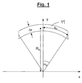
- the illumination systems pursuant to the invention described below illuminate a segment of a ring field as shown in Figure 1.
- An arc shaped field 11 in a reticle plane is imaged into a wafer plane by a projection objective.
- the width of the arc shaped field 11 is ⁇ r and the mean radius is R 0 .
- the arc shaped field extends over an angular range of 2 ⁇ 0 and an arc of 2 ⁇ s 0 .
- the angle ⁇ 0 is defined from the y-axis to the field edge, the arc length s 0 is defined from the center of the field to the field edge along the arc at the mean radius R 0 .
- the scanning energy SE(x) at x is found to be the line integral over the intensity E(x,y) along the scan direction, which is the y-direction in this embodiment: in which E(x,y) is the intensity distribution in the x-y plane.
- Each point on the reticle or wafer contains the scanning energy SE(x) corresponding to its x coordinate. If uniform exposure is desired, it is advantageous for the scanning energy to be largely independent of x. In photolithography, it is desirable to have a uniform scanning energy distribution in the wafer plane.
- the resist on the wafer is very sensitive to the level of light striking the wafer plane.
- each point on the wafer receives the same quantity of light or the same quantity of scanning energy.
- the scanning energy can be controlled by the design of the field lens group.
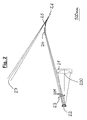
- an EUV illumination system is shown in Figure 2.
- the light of the source is collected with an ellipsoidal mirror 21 and directed to a first mirror 22 comprising several rectangular mirror elements.
- the single mirror elements are called field facets, because they are imaged in an image plane 26 of the illumination system.
- the field facets are plane mirror elements in which each field facet is tilted by a different amount.
- the ellipsoidal mirror 21 images the light source 200 in an aperture stop plane 23.
- the image of the light source is divided into several secondary light sources 201 so that the number of secondary light sources 201 depends on the number of tilted field facets.
- the secondary light sources 201 are imaged in an exit pupil 27 of the illumination system using a field mirror 24 and a field mirror 25.
- the location of the exit pupil 27 depends on the design of the projection objective, which is not shown in Figure 2.
- the field mirrors 24 and 25 are grazing incidence mirrors with a toroidal shape.
- the imaging of the field facets in the image plane 26 is influenced by the field mirrors 24 and 25. They introduce distortion to shape the arc shaped images of the rectangular field facets and to control the illumination intensity in the plane of the image plane 26, where a reticle is typically located. This will be further explained below.
- the tilt angles of the field facets are chosen to overlay the arc shaped images of the field facets at least partly in the image plane 26.
- the embodiment of Figure 2 is only an example.
- the source is not limited to Laser-Produced-Plasma sources. Lasers for wavelength ⁇ 193nm, Pinch Plasma sources, synchrotrons, wigglers or undulators for wavelength between 10-20nm are also possible light sources.
- the collector unit is adapted for the angular and spatial characteristic of the different light sources.
- the illumination system does not need to be purely reflective. Catadioptric or dioptric components are also possible.
- Figure 3 shows, in a schematic three-dimensional view, the imaging of one field facet 31 to an image plane 35.
- the beam path of this central field facet 31 located on the optical axis is representative of all other field facets.
- An incoming beam 300 is focused to a secondary light source 301 using the field facet 31.
- the field facet 31 is in this case a concave mirror element.
- the secondary light source 301 is spot-like if a point source is used.
- the beam diverges after the secondary light source 301. Without a field mirror 33 and a field mirror 34, the image of the rectangular field facet 31 would be rectangular.
- the imaging of the field facet 31 is distorted to produce an arc shaped field 302. The distortion is provided by the field mirrors 33 and 34.
- a reflected beam 303 is focused at the exit pupil of the illumination system using the field mirrors 33 and 34.
- the exit pupil is not shown in Figure 3.
- the field mirrors 33 and 34 image the secondary light source 301 into the exit pupil.
- the secondary light source 301 is extended. To get a sharp image of the field facet 31 it is advantageous to image the field facet 31 into the image plane 35 using another mirror 32.
- the mirror 32 located at the secondary light source 301 is called a pupil facet and has a concave surface. Each secondary light source has such a pupil facet.
- Figure 3 shows a light path for one pair of field facet 31 and pupil facet 32.
- the plurality of mirror elements 32 forms another faceted mirror.
- the term "entendue” refers to a phase-space volume of a light source. Pupil facets are necessary only for extended light sources, which have a high luminae value. In the case of a point source, the secondary light source is also a point, and a pupil facet would have no influence on the imaging.
- the source diameter of the Laser-Produced-Plasma source 200 is only 50 ⁇ m, so the pupil facets are not required.
- the mirror with the pupil facets is added at the aperture stop plane 23. To eliminate vignetting, the tilt angle of the mirror 22 with the field facets is increased.
- the field mirrors 24, 25, 33, 34 shown in Figures 2 and 3 form the arc shaped field 302, image the plane of the aperture stop 23 in the exit pupil plane 27 of the illumination system, and control the illumination distribution in the arc shaped field 302.
- the imaging of the central field facet 31 shown in Figure 3 is used to optimize the design of the field mirrors 33 and 34.
- the form of the images of other field facets is determined by a field lens group nearly in the same way as for the central field facet 31.
- the design of the field lens group which in turn controls the scanning energy, can be optimized through the imaging of the central field facet 31.
- This facet can be considered as a homogeneously radiating surface. In the real system with all field facets homogeneity results from the superimposition of the images of all field facets.
- the goals include controlling the scanning energy, producing an arc shaped field, and imaging of the plane with secondary light sources to an exit pupil of the illumination system.
- the given components include a first mirror with field facets 31, a second mirror with pupil facets 32, a field lens group including mirror 33 and mirror 34, image plane 35 and an exit pupil plane (not shown in Figure 3).
- the field lens group in this case the shapes of mirror 33 and mirror 34, will be designed. Without the field lens group, the shape of the illuminated field in image plane 35 would be rectangular, the illuminated field would not be distorted, and there would be no pupil imaging.
- the complexity of the process of designing the field lens group is reduced by considering the imaging of only the central field facet 31, rather than considering all of the facets. Facet 31 is imaged to image plane 35 using pupil facet 32.
- the design of the field lens group requires (1) controlling the scanning energy by introducing distortion perpendicular to the scanning direction, (2) producing an arc shaped field, and (3) imaging the secondary light sources 301 to the exit pupil of the illumination system.
- the field lens group only influences the field facet imaging by distorting this imaging.
- the main component of the field facet imaging is due to the pupil facet 32 (or to a camera obscura).
- a simulation is constructed for all the field facets, the pupil facets and the field lens group designed in the first step.
- the field lens group influences the imaging of the other field facets in a manner similar to that of the imaging of the central field facet. If the imaging is not similar, the design of the field lens group must be corrected. Such corrections are typically small.
- a superimposition of the images of all field facets results in intensity homogeneity in the image plane. This is similar to the principle of a fly-eye integrator. Since the central field facet is representative of all field facets, design complexity is reduced by considering only the central field facet. To simulate the intensity distribution in the image plane only with a central light channel defined by field facet 31 and pupil facet 32, the central field facet 31 is regarded as a homogeneous radiating surface.
- Figure 4 shows, schematically, an imaging of a rectangular field 41 on an arc shaped field 42 at an image plane of an illumination system.
- the rectangular field 41 can be a homogeneously radiating real or virtual surface in a plane conjugated to a reticle plane.
- Figure 4 shows the correlation between rectangular field 41 and arc shaped field 42, and it also shows the orientation and definition of the coordinate system.
- the description of the scanning energy control, as set forth in the following pages, is independent of the design layout of the field facets or pupil facets. Accordingly, only a homogeneously radiating rectangular field is being considered.
- the rectangular field is given by central field facet 31.
- a length x w at the rectangular field 41 is imaged on an arc length s at the arc shaped field 42, and a length y w is imaged on a radial length r.
- the origin of the coordinate systems is the center of the field for the rectangular field 41 and the optical axis for the arc shaped field 42.
- the image formation can be divided into two components ⁇ s and ⁇ rad : ⁇ s : x w ⁇ s ⁇ rad : y w ⁇ r wherein
- the scanning energy SE(x r ) in the plane of the reticle is a function of x r
- the rise of the scanning energy toward the edge of the field is considerably smaller for larger radius R 0 of the arc shaped field 42 and smaller arc angles ⁇ 0 .
- the intensity E r v (x r ) in the plane of the reticle can be controlled by varying the quotient ds V / dx w .
- the intensity E(x r ,y r ) can be written as the product of the functions g(r) and f(s).
- g(r) should be independent of the x-position x r in the plane of the reticle and f(s) should be independent of the y-position y r in the plane of the reticle.
- SE(x r ) can also be written as a function of s:
- the scanning energy can thus be set directly, with x r being the x-component of a field point on the arc shaped field 42 and x w being the x-component of a field point on the rectangular field 41.
- the azimuthal imaging magnification ⁇ s can be calculated with these formulas.
- the azimuthal imaging magnification is derived as follows: and thus
- Rectangular field 41 in a plane conjugated to the plane of the reticle is
- Arc shaped field 42 in the plane of the reticle is
- the field lens group in addition to field formation, also determines the imaging of the secondary light sources, or the aperture stop plane, into the entrance pupil of the projection objective. This as well as the geometric boundary conditions does not permit an arbitrarily large distortion correction.
- the previously described uniformity correction is not restricted to the illumination system with a faceted mirror described by way of example, but can be used in general.
- the intensity distribution By distorting the image formation in the reticle plane perpendicular to the scanning direction the intensity distribution, and thus the scanning energy distribution, can be controlled.
- the illumination system contains a real or virtual plane with secondary light sources. This is always the case, in particular, with Kohler illumination systems.
- the aforementioned real or virtual plane is imaged in the entrance pupil of the objective using the field lens group, with the arc shaped field being produced in the pupil plane of this image formation.
- the pupil plane of the pupil imaging is, in this case, the plane of the reticle.
- the solid angle ⁇ of the collected radiation is ⁇ 2 ⁇ .
- the mirror 22 with field facets has a diameter of 70.0mm, and the plane field facets have a rectangular shape with x-y dimensions of 17.5mm x 1.0mm.
- the mirror 22 consists of 220 field facets. Each facet is tilted relative to the local x- and y-axis to overlay the images of the field facets at least partly in the image plane 26.
- the field facets at the edge of mirror 22 have the largest tilt angles in the order of 6°.
- the aperture stop plane 23 in this example is not accessible.
- the first and second field mirrors 24 and 25 are grazing incidence mirrors. Each of them bends the optical axis by 160°.
- the field mirror 24 is a concave mirror
- the mirror 25 is a convex mirror. They are optimized to control the illumination intensity, the field shaping and the pupil imaging. In the following embodiments only these two mirrors will be replaced. Their position and tilt angle will always be the same. It will be shown, that by modifying the surface shape, it is possible to change the intensity distribution while keeping the pupil imaging and the field shaping in tolerance.
- the arc shaped field in the plane of the reticle 26 can be described by
- the position of the exit pupil 27 of the illumination system is defined by the given design of the projection objective.
- a notable feature of the present invention is the asphericity of the mirror surfaces that provide a favorable uniformity of scanning energy on the one hand, and on the other hand a favorable telecentricity. While the asphericity of the mirror surfaces will be varied, the tilt angles and spacing of the mirrors are to be kept constant.
- Both field mirrors are toroidal mirrors with surface parameters defined in the x- and y-direction.
- R describes the Radius
- K the conical constant. It is also possible to vary higher aspherical constants, but in the examples shown below only the radii and conical constants will be varied.
- the curve of the scanning energy over the x direction in the plane of the reticle is plotted in Figure 5 as a solid line 51. Because the system is symmetric to the y-axis, only the positive part of the curve is shown.
- the scanning energy is normalized at the center of the field at 100%. The scanning energy rises toward the edge of the field to 124%.
- the calculation takes into consideration only the imaging of one representative field facet, in this case the central field facet, which is assumed to be a homogenous radiating surface.
- the curves of Figure 6 are the result of a simulation with a Laser-produced-Plasma source 200 and the whole illumination system according to Figure 2.
- the solid line 61 represents the scanning energy for toroidal field mirrors of the 1st embodiment without conic constants.
- the dashed curve 52 in Figure 5 shows the curve of scanning energy expected from the design for the central field facet; the curve scanning energy obtained with the entire system of all of the field facets is shown as dashed curve 62 in Figure 6.
- the improvement of the scanning uniformity is obvious using the conical constants in the design of the field mirrors.
- the necessary surface corrections on the two field mirrors 24 and 25 of Figure 2 are shown in the illustrations of Figure 7 and Figure 8 as contour plots.
- the mirrors are bounded according to the illuminated regions on the mirrors.
- the bounding lines are shown as reference 71 in Figure 7 and reference 81 in Figure 8.
- the contour plots show the sagitta differences of the surfaces of the first and second embodiment in millimeters.
- the maximum sagitta difference is on the order of magnitude of 0.4mm in Figure 7. There is also a sign reversal of the sagitta differences.
- the second embodiment was optimized to get the best improvement of the scanning uniformity accepting an arising telecentricity error.
- the telecentricity violation of 1.77mrad in the reticle plane of the second embodiment is problematic for a lithographic system.
- the design shown in the example of embodiment 1 is the starting point for the design of the field mirrors in the following examples. In each example, different sets of surface parameters have been optimized.
- Table 2 shows that field mirror 1 and field mirror 2 improve the scanning uniformity to almost the same extent, with the principal fraction of this being carried by the x parameters, which ultimately determine the azimuthal magnification scale ⁇ s .
- Actuation in this case can occur by means of mechanical actuators.
- a possible actuator can be a piezo-element at the rear side of a field mirror to vary the shape of the mirror by changing the voltage to the piezo-element.
- great improvements of uniformity can be produced even when only the x surface parameters are changed. If only the conic constants in the x direction are varied, the sagitta differences have the same algebraic sign over the entire surface, which is advantageous for the surface manipulation.
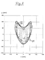
- Figure 9 and Figure 10 show the sagitta differences between the field mirrors of embodiment #6 and embodiment #1.
- the conic constants in the x direction were varied here for field mirror 1 and 2.
- the maximum sagitta differences are 250 ⁇ m for the first field mirror 24 and 100 ⁇ m for the second field mirror 25.
- Uniformity is improved from 10.7% to 7.0% with an additional telecentricity violation of 1.0 mrad in the plane of the reticle.
- pfh ref (x,y) 1 R x ⁇ x 2 + 1 R y ⁇ y 2 1+ 1- 1 R x ⁇ x 2 - 1 R y ⁇ y 2 x and y are the mirror coordinates in the local coordinate system of the mirror surface.
- R x and R y are the radii of the toroidal mirror.
- pfh ref (x,y) 1 R x ⁇ x 2 + 1 R y ⁇ y 2 1+ 1-(1+K x ) ⁇ 1 R x ⁇ x 2 -(1+K y ) ⁇ 1 R y ⁇ y 2 K x and K y are the conical constants.
- the actuators or mechanical regulators are placed on the mirrors on equipotential lines 92, 102 (sites of equal sagitta difference).
- these rows of identical actuators run almost parallel to the y axis, and therefore, it is unnecessary to control a two-dimensional field of actuators, but it suffices to control only a row of different actuator banks.
- the second field mirror an arrangement of actuator rows can be proposed as shown in Figure 11.
- the second field mirror is shown in the plan view (x-y-view) at the top and side view (x-z-view) at the bottom of Figure 11.
- the actuator beams 5', 4', 3', 2', 1', 0, 1, 2, 3, 4, 5 are arranged along equipotential lines. Because of the symmetry regarding the y-axis the corresponding actuator beams 5 and 5', or 4 and 4', or 3 and 3', or 2 and 2', or 1 and 1' can be activated with the same signal.
- the actuators in the plan view are represented by lines, and in the side view by arrows.
- An industrial implementation would be to design the entire row of actuators as actuator beams 5', 4', 3', 2', 1', 0, 1, 2, 3, 4, 5.
- the entire row of actuators is raised or lowered.
- the distances between the actuator beams can be chosen dependent on the gradient of the sagitta differences. For high values of the gradient a dense arrangement of the actuator beams is necessary, for low values of the gradient the distances can be increased. In the example of Figure 10 the gradient of the sagitta differences is high at the edges of the illuminated field, so more actuator beams are at the edge of the field than in the center as shown in Figure 11.
- An active correction of uniformity can be accomplished as follows using the actuators described above.
- the curve of scanning energy SE Standard (x r ) in the plane of the reticle is established based on the geometric design of the field lens group.
- the scanning energy SE wafer (x wafer ) in the plane of the wafer is measured, including all coating, absorption, and vignetting effects.
- SE water (x wafer ) has to be independent of the x-position x w in the plane of the wafer. If this is not the case, the x w -dependent offset has to be addressed by the illumination system.
- SE wafer (x wafer ) can be converted directly into the plane of the reticle SE wafer (x r ) using the given magnification of the projection objective.
- SE akt Des (x r ) SE wafer (x r ) - SE Standard (x r ) SE akt / Des (x r ) determines the azimuthal magnification ⁇ s , and from this the necessary corrections for the field lens group.
- the uniformity of the scanning energy can be corrected by the actuators described above within certain limits. Up to + 2.5% uniformity can be corrected with one manipulable field mirror, and up to ⁇ 5.0% with two manipulable field mirrors.
- Intensity loss-free control of scanning energy is achieved by the present invention, where the field-dependent scan path, the coating, absorption, and vignetting effects, if known, can be taken into account in the static design of the field lens group. Furthermore, the invention proposes dynamic control with active field mirrors for time-dependent or illumination setting-dependent effects. If a telecentricity error of ⁇ 4.0 mrad is allowed in the plane of the wafer, the uniformity correction can be up to + 5%.
- a projection exposure system comprising an Laser-Produced-Plasma source as light source 120, an illumination system 121 corresponding to the invention, a mask 122, also known as a reticle, a positioning system 123, a projection objective 124 and a wafer 125 to be exposed on a positioning table 126 is shown.
- the projection objective 124 for EUV lithography is typically a mirror system with an even number of mirrors to have reticle and wafer on different sides of the projection objective 124.
- Detection units in a reticle plane 128 and in a wafer plane 129 are provided to measure the intensity distribution inside the illuminated field.
- the measured data are transferred to a computation unit 127. With the measured data the scanning energy and scanning uniformity can be evaluated. If there is a difference between the predetermined and the measured intensity distribution, the surface corrections are computed.
- the actuator drives 130 at one of the field mirrors are triggered to manipulate the mirror surface.
Landscapes
- Physics & Mathematics (AREA)
- General Physics & Mathematics (AREA)
- Spectroscopy & Molecular Physics (AREA)
- Engineering & Computer Science (AREA)
- General Engineering & Computer Science (AREA)
- High Energy & Nuclear Physics (AREA)
- Exposure And Positioning Against Photoresist Photosensitive Materials (AREA)
- Exposure Of Semiconductors, Excluding Electron Or Ion Beam Exposure (AREA)
- Microscoopes, Condenser (AREA)
Applications Claiming Priority (2)
| Application Number | Priority Date | Filing Date | Title |
|---|---|---|---|
| DE19908526A DE19908526A1 (de) | 1999-02-26 | 1999-02-26 | Beleuchtungssystem mit Feldspiegeln zur Erzielung einer gleichförmigen Scanenergie |
| DE19908526 | 1999-02-26 |
Publications (2)
| Publication Number | Publication Date |
|---|---|
| EP1031882A2 true EP1031882A2 (de) | 2000-08-30 |
| EP1031882A3 EP1031882A3 (de) | 2003-10-29 |
Family
ID=7899072
Family Applications (1)
| Application Number | Title | Priority Date | Filing Date |
|---|---|---|---|
| EP00104014A Withdrawn EP1031882A3 (de) | 1999-02-26 | 2000-02-25 | Beleuchtungssystem mit Feldspiegeln zur Erzeugung einer gleichmässigen Abtastenergie |
Country Status (6)
| Country | Link |
|---|---|
| US (1) | US6770894B1 (de) |
| EP (1) | EP1031882A3 (de) |
| JP (1) | JP2000252208A (de) |
| KR (1) | KR20000058210A (de) |
| DE (1) | DE19908526A1 (de) |
| TW (1) | TW440748B (de) |
Cited By (3)
| Publication number | Priority date | Publication date | Assignee | Title |
|---|---|---|---|---|
| WO2002027400A3 (en) * | 2000-09-29 | 2002-07-11 | Zeiss Carl | Illumination system particularly for microlithography |
| EP1724641A1 (de) * | 2005-05-20 | 2006-11-22 | Infineon Technologies AG | Lithographischer Projektionsapparat und Methode zur Belichtung eines Halbleiterwafers mit dem Muster einer Maske |
| EP1469349B1 (de) * | 2003-04-17 | 2011-10-05 | ASML Netherlands B.V. | Lithographische Projektionsvorrichtung mit einem einen Konkavspiegel und einen Konvexspiegel aufweisenden Kollektor |
Families Citing this family (7)
| Publication number | Priority date | Publication date | Assignee | Title |
|---|---|---|---|---|
| EP1890191A1 (de) * | 2006-08-14 | 2008-02-20 | Carl Zeiss SMT AG | Katadioptrisches Projektionsobjektiv mit einem Pupillenspiegel |
| EP1950594A1 (de) * | 2007-01-17 | 2008-07-30 | Carl Zeiss SMT AG | Abbildende Optik, Projektionsbelichtunsanlage für die Mikrolithographie mit einer derartigen abbildenden Optik, Verfahren zur Herstellung eines mikrostrukturierten Bauteils mit einer derartigen Projektionsbelichtungsanlage, durch das Herstellungsverfahren gefertigtes mikrostrukturiertes Bauelement sowie Verwendung einer derartigen abbildenden Optik |
| KR101542272B1 (ko) * | 2007-10-26 | 2015-08-06 | 칼 짜이스 에스엠티 게엠베하 | 결상 광학 시스템 및 이러한 유형의 결상 광학 시스템을 구비하는 마이크로리소그래피용 투영 노광 장치 |
| CN101978324B (zh) | 2008-03-20 | 2013-04-03 | 卡尔蔡司Smt有限责任公司 | 用于微光刻的投射物镜 |
| DE102009006685A1 (de) * | 2009-01-29 | 2010-08-05 | Carl Zeiss Smt Ag | Beleuchtungssystem für die Mikro-Lithographie |
| KR101478400B1 (ko) * | 2009-03-06 | 2015-01-06 | 칼 짜이스 에스엠티 게엠베하 | 조명 광학 시스템 및 마이크로리소그래피용 광학 시스템 |
| DE102014218474A1 (de) * | 2014-09-15 | 2016-03-17 | Carl Zeiss Smt Gmbh | Projektionsobjektiv, Projektionsbelichtungsanlage und Projektionsbelichtungsverfahren für die EUV-Mikrolithographie |
Family Cites Families (18)
| Publication number | Priority date | Publication date | Assignee | Title |
|---|---|---|---|---|
| US4883352A (en) * | 1984-06-21 | 1989-11-28 | American Telephone And Telegraph Company | Deep-uv lithography |
| JPH02180013A (ja) | 1989-01-05 | 1990-07-12 | Nippon Telegr & Teleph Corp <Ntt> | X線投影露光装置 |
| US5222112A (en) | 1990-12-27 | 1993-06-22 | Hitachi, Ltd. | X-ray pattern masking by a reflective reduction projection optical system |
| US5640284A (en) | 1992-09-11 | 1997-06-17 | Nikon Corporation | Optical reflector, illumination optical system, light source system and illumination optical apparatus |
| US5339346A (en) | 1993-05-20 | 1994-08-16 | At&T Bell Laboratories | Device fabrication entailing plasma-derived x-ray delineation |
| US6229595B1 (en) * | 1995-05-12 | 2001-05-08 | The B. F. Goodrich Company | Lithography system and method with mask image enlargement |
| US5805365A (en) | 1995-10-12 | 1998-09-08 | Sandia Corporation | Ringfield lithographic camera |
| DE19548805A1 (de) * | 1995-12-27 | 1997-07-03 | Zeiss Carl Fa | REMA-Objektiv für Mikrolithographie-Projektionsbelichtungsanlagen |
| US5737137A (en) | 1996-04-01 | 1998-04-07 | The Regents Of The University Of California | Critical illumination condenser for x-ray lithography |
| JP3862347B2 (ja) | 1996-04-11 | 2006-12-27 | キヤノン株式会社 | X線縮小露光装置およびこれを利用したデバイス製造方法 |
| JPH1152289A (ja) | 1997-08-05 | 1999-02-26 | Minolta Co Ltd | 二次元照明光学系及びこれを用いた液晶プロジェクター |
| US5844727A (en) * | 1997-09-02 | 1998-12-01 | Cymer, Inc. | Illumination design for scanning microlithography systems |
| US5920380A (en) * | 1997-12-19 | 1999-07-06 | Sandia Corporation | Apparatus and method for generating partially coherent illumination for photolithography |
| US6144495A (en) * | 1997-12-23 | 2000-11-07 | Canon Kabushiki Kaisha | Projection light source |
| JP4238390B2 (ja) | 1998-02-27 | 2009-03-18 | 株式会社ニコン | 照明装置、該照明装置を備えた露光装置および該露光装置を用いて半導体デバイスを製造する方法 |
| EP0955641B1 (de) * | 1998-05-05 | 2004-04-28 | Carl Zeiss | Beleuchtungssystem insbesondere für die EUV-Lithographie |
| US6195201B1 (en) | 1999-01-27 | 2001-02-27 | Svg Lithography Systems, Inc. | Reflective fly's eye condenser for EUV lithography |
| US6215128B1 (en) * | 1999-03-18 | 2001-04-10 | Etec Systems, Inc. | Compact photoemission source, field and objective lens arrangement for high throughput electron beam lithography |
-
1999
- 1999-02-26 DE DE19908526A patent/DE19908526A1/de not_active Withdrawn
-
2000
- 2000-02-11 TW TW089102315A patent/TW440748B/zh not_active IP Right Cessation
- 2000-02-25 US US09/514,040 patent/US6770894B1/en not_active Expired - Fee Related
- 2000-02-25 EP EP00104014A patent/EP1031882A3/de not_active Withdrawn
- 2000-02-26 KR KR1020000009616A patent/KR20000058210A/ko not_active Abandoned
- 2000-02-28 JP JP2000052551A patent/JP2000252208A/ja active Pending
Cited By (3)
| Publication number | Priority date | Publication date | Assignee | Title |
|---|---|---|---|---|
| WO2002027400A3 (en) * | 2000-09-29 | 2002-07-11 | Zeiss Carl | Illumination system particularly for microlithography |
| EP1469349B1 (de) * | 2003-04-17 | 2011-10-05 | ASML Netherlands B.V. | Lithographische Projektionsvorrichtung mit einem einen Konkavspiegel und einen Konvexspiegel aufweisenden Kollektor |
| EP1724641A1 (de) * | 2005-05-20 | 2006-11-22 | Infineon Technologies AG | Lithographischer Projektionsapparat und Methode zur Belichtung eines Halbleiterwafers mit dem Muster einer Maske |
Also Published As
| Publication number | Publication date |
|---|---|
| KR20000058210A (ko) | 2000-09-25 |
| EP1031882A3 (de) | 2003-10-29 |
| TW440748B (en) | 2001-06-16 |
| JP2000252208A (ja) | 2000-09-14 |
| DE19908526A1 (de) | 2000-08-31 |
| US6770894B1 (en) | 2004-08-03 |
Similar Documents
| Publication | Publication Date | Title |
|---|---|---|
| US6859515B2 (en) | Illumination system, particularly for EUV lithography | |
| US6400794B1 (en) | Illumination system, particularly for EUV lithography | |
| KR100648101B1 (ko) | Euv- 리소그래피용 조명장치 | |
| KR101515663B1 (ko) | 결상 광학 시스템 및 이러한 유형의 결상 광학 시스템을 갖는 마이크로리소그래피용 투영 노광 장치 | |
| KR101386353B1 (ko) | 푸리에 광학 시스템을 포함하는 조명 시스템 | |
| TWI714278B (zh) | 投影透鏡、投影曝光裝置、與euv微影的投影曝光方法 | |
| KR101401227B1 (ko) | 편향 미러를 포함하는 반사 굴절식 투영 대물 렌즈 및 투영 노광 방법 | |
| US11181826B2 (en) | Projection exposure method and projection exposure apparatus for microlithography | |
| EP1523699A2 (de) | Projektionsobjektiv für eine projektionsbelichtungsvorrichtung | |
| EP1031882A2 (de) | Beleuchtungssystem mit Feldspiegeln zur Erzeugung einer gleichmässigen Abtastenergie | |
| US20020141071A1 (en) | Illumination system with reduced heat load | |
| US7126137B2 (en) | Illumination system with field mirrors for producing uniform scanning energy | |
| KR102408217B1 (ko) | 투영 노광 방법 및 투영 노광 장치 | |
| US20070030948A1 (en) | Illumination system with field mirrors for producing uniform scanning energy | |
| US9612540B2 (en) | Method of operating a microlithographic apparatus | |
| JP5959021B2 (ja) | 投影対物器械を製造する方法及びこの方法によって製造される投影対物器械 | |
| JP2000098228A (ja) | 投影露光装置及び露光方法、並びに反射縮小投影光学系 | |
| US8300211B2 (en) | Catadioptric projection objective | |
| JP2000100703A (ja) | 投影露光装置及び方法、並びに反射縮小投影光学系 | |
| EP4592749A1 (de) | Lithographischer apparat und zugehöriges verfahren |
Legal Events
| Date | Code | Title | Description |
|---|---|---|---|
| PUAI | Public reference made under article 153(3) epc to a published international application that has entered the european phase |
Free format text: ORIGINAL CODE: 0009012 |
|
| AK | Designated contracting states |
Kind code of ref document: A2 Designated state(s): AT BE CH CY DE DK ES FI FR GB GR IE IT LI LU MC NL PT SE |
|
| AX | Request for extension of the european patent |
Free format text: AL;LT;LV;MK;RO;SI |
|
| PUAL | Search report despatched |
Free format text: ORIGINAL CODE: 0009013 |
|
| AK | Designated contracting states |
Kind code of ref document: A3 Designated state(s): AT BE CH CY DE DK ES FI FR GB GR IE IT LI LU MC NL PT SE |
|
| AX | Request for extension of the european patent |
Extension state: AL LT LV MK RO SI |
|
| 17P | Request for examination filed |
Effective date: 20040219 |
|
| AKX | Designation fees paid |
Designated state(s): DE FR GB NL |
|
| RAP1 | Party data changed (applicant data changed or rights of an application transferred) |
Owner name: CARL ZEISS SMT AG |
|
| GRAP | Despatch of communication of intention to grant a patent |
Free format text: ORIGINAL CODE: EPIDOSNIGR1 |
|
| RAP1 | Party data changed (applicant data changed or rights of an application transferred) |
Owner name: CARL ZEISS SMT AG |
|
| STAA | Information on the status of an ep patent application or granted ep patent |
Free format text: STATUS: THE APPLICATION IS DEEMED TO BE WITHDRAWN |
|
| 18D | Application deemed to be withdrawn |
Effective date: 20051118 |