EP1031995A1 - Speicherschaltung mit eingebautem Selbsttest - Google Patents
Speicherschaltung mit eingebautem Selbsttest Download PDFInfo
- Publication number
- EP1031995A1 EP1031995A1 EP99103479A EP99103479A EP1031995A1 EP 1031995 A1 EP1031995 A1 EP 1031995A1 EP 99103479 A EP99103479 A EP 99103479A EP 99103479 A EP99103479 A EP 99103479A EP 1031995 A1 EP1031995 A1 EP 1031995A1
- Authority
- EP
- European Patent Office
- Prior art keywords
- address
- test
- self
- built
- memory device
- Prior art date
- Legal status (The legal status is an assumption and is not a legal conclusion. Google has not performed a legal analysis and makes no representation as to the accuracy of the status listed.)
- Granted
Links
- 238000012360 testing method Methods 0.000 title claims abstract description 64
- 230000015654 memory Effects 0.000 title claims description 23
- 230000003111 delayed effect Effects 0.000 claims description 9
- 230000004044 response Effects 0.000 claims description 5
- 230000006870 function Effects 0.000 claims description 3
- 230000003068 static effect Effects 0.000 claims description 2
- 238000000034 method Methods 0.000 abstract description 15
- 238000013461 design Methods 0.000 abstract description 4
- 230000015572 biosynthetic process Effects 0.000 abstract description 3
- 230000008569 process Effects 0.000 abstract description 3
- 238000003786 synthesis reaction Methods 0.000 abstract description 3
- 238000005516 engineering process Methods 0.000 abstract description 2
- 210000004027 cell Anatomy 0.000 description 16
- 238000003780 insertion Methods 0.000 description 3
- 230000037431 insertion Effects 0.000 description 3
- 238000012546 transfer Methods 0.000 description 3
- 230000007704 transition Effects 0.000 description 3
- 238000013459 approach Methods 0.000 description 2
- 125000004122 cyclic group Chemical group 0.000 description 2
- 238000005457 optimization Methods 0.000 description 2
- 230000009466 transformation Effects 0.000 description 2
- 210000004460 N cell Anatomy 0.000 description 1
- 238000004458 analytical method Methods 0.000 description 1
- 230000015556 catabolic process Effects 0.000 description 1
- 230000008859 change Effects 0.000 description 1
- 230000007547 defect Effects 0.000 description 1
- 238000006731 degradation reaction Methods 0.000 description 1
- 230000001934 delay Effects 0.000 description 1
- 238000010586 diagram Methods 0.000 description 1
- 239000000428 dust Substances 0.000 description 1
- 238000011990 functional testing Methods 0.000 description 1
- 238000004519 manufacturing process Methods 0.000 description 1
- 230000008450 motivation Effects 0.000 description 1
- 239000002245 particle Substances 0.000 description 1
- 238000013519 translation Methods 0.000 description 1
Images


Classifications
-
- G—PHYSICS
- G11—INFORMATION STORAGE
- G11C—STATIC STORES
- G11C29/00—Checking stores for correct operation ; Subsequent repair; Testing stores during standby or offline operation
- G11C29/04—Detection or location of defective memory elements, e.g. cell constructio details, timing of test signals
- G11C29/08—Functional testing, e.g. testing during refresh, power-on self testing [POST] or distributed testing
- G11C29/12—Built-in arrangements for testing, e.g. built-in self testing [BIST] or interconnection details
- G11C29/36—Data generation devices, e.g. data inverters
-
- G—PHYSICS
- G01—MEASURING; TESTING
- G01R—MEASURING ELECTRIC VARIABLES; MEASURING MAGNETIC VARIABLES
- G01R31/00—Arrangements for testing electric properties; Arrangements for locating electric faults; Arrangements for electrical testing characterised by what is being tested not provided for elsewhere
- G01R31/28—Testing of electronic circuits, e.g. by signal tracer
- G01R31/317—Testing of digital circuits
- G01R31/3181—Functional testing
- G01R31/31813—Test pattern generators
Definitions
- the invention relates to a test and a test hardware of a memory. More particularly, the invention relates to a built-in self-test circuit for memories embedded on the same chip.
- Memories are susceptible to fabrication process related failures caused by dust particles on the chips or masks, scratches and gate oxide pinholes, which may results open or short circuits. Many methods or hardwares have been developed to test whether a memory can function normally. However, as the integrated circuit art becomes more and more advanced, functions of memories become much more and more complex. Consequently, it often takes a great time and requires a complex circuit to perform a functional test of the memories.
- BIST built-in self-test
- a test algorithm is translated into a sequence of commands, data, and addresses applied to the memory under test.
- FSM hard-wired finite state machine
- the BIST circuit operates as fast as the memory under test.
- a disadvantage of the approach is that the finite state machine is tailored to a specific set of test patterns whose complexity depends on the test algorithm. As the complexity of the test algorithm increases, this approach may be inadequate because the finite state machine may become too large and too slow to produce a test pattern in each clock cycle to intensively exercise the memory under test.
- Some BIST circuits known to be the programmable or configurable BIST circuits, can be referred to U.S. Patent No. 5,173,906, "Built-in Self-Test for Integrated Circuit” disclosed by Dreibelbis et al, in 1992.
- Another disclosure of a circuit that uses a micro-coded sequence defined in the contents of a read-only memory to produce the test patterns is issued with a US Patent No. 5,224,101 to Popyack et al in 1993.
- US Patent No. 5,301,156 "Configurable Self-Test for Embedded RAMs”.
- Talley et al discloses a circuit that has a serial path which passes through the address, command, and data portions of the circuit to shift in a test or control pattern and to shift out the results, each scan requiring several clock cycles.
- the invention provides a circuit and a method for testing a memory, especially for testing of a memory device.
- the circuit comprises a pattern generator, a built-in self-test output buffer, a delay buffer, and a comparator.
- the pattern generator further comprises three modules, a finite state machine to generate data and commands of test patterns, an address generator to perform address computation, and a prediction logic to predict an address of a next clock cycle based on the address information of a previous cycle.
- the invention adapts a cyclic path breaking technique.
- the original critical path is broken into segments.
- the clock-cycle time of the pattern generator is thus dominated by a longest clock-cycle time among these segments.
- clock cycles are delayed.
- a prediction logic is inserted between flip-flops. As a consequence, the latency caused by the insertion of flip-flops is resolved, while the clock-cycle time of the pattern generator is effectively reduced.
- a test algorithm written as a program in a high-level language is often proposed.
- a memory device comprising R rows and C columns is to be tested, four steps are included in a march algorithm.
- a first step '0' is written to every cell.
- the second step walks through the entire array in a forward manner, that is, from the first cell in the first row to the last cell in the last row.
- a so-called READ(0)-WRITE(1)-READ(1) operation is performed.
- This READ-WRITE-READ operation is proposed in an attempt to better expose the potential dynamic defects of the memory cells.
- the third step walks through the entire cell from the last cell to the first cell. At each cell, a READ(1)-WRITE(0)-READ(0) operation is performed.
- the fourth step of this algorithm checks if the value of every cell is still zero after the first three steps.
- the built-in self-test circuit comprises a pattern generator, a built-in self-test circuit (BIST) output buffer (BOB), a delay buffer and a comparator.
- the pattern generator is a finite state machine which produces a sequence of test patterns. This relates to the above test algorithm.
- the BOB is a buffer between the BIST circuit and the memory device, for example, an SRAM, to eliminate the potential degradation of the memory device due to the introduction of the BIST circuit.
- the delay buffer is a first-in-first-out register file between pattern generator and the comparator. It is primarily for computing the expected response of the memory read command. The number of delayed clock cycles depends on the latency of the READ operation of the memory.
- the comparator is a piece of combinational logic that compares the output responses of the memory with the expected values to determine if the memory is functionally correct, where the expected values are provided by the delay buffer.
- the pattern generator is the timing critical one that dominates the clock-cycle time.
- the technique to break a timing critical path is to be described in the following paragraphs.
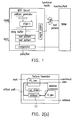
- Fig. 2(a) to Fig. 2(c) shows an evolvement of a pattern generator in a built-in self-test circuit as shown in Fig. 1 according to the invention.
- Fig. 2(a) shows a structure of a naive pattern generator.
- the pattern generator is responsible for generating test patterns each of which comprises portions of data, commands, and addresses.
- the pattern generator can thus be further divided into two modules, that is, a finite state machine denoted as PG_fsm and an address generator denoted as A_gen .
- the module PG_fsm generates the command portion and the data portion of the test patterns, as well as an address command, denoted as a_command.
- the address command a_command is used to drive the module A_gen , which is responsible for generating the address portion of each test pattern.
- nine address commands are used to accommodate various test algorithms. These nine address commands include NO_CHANGE, INIT_ADDRESS, LAST_ADDRESS, NEXT_CELL, PREVIOUS_CELL, Y_NEXT_CELL, Y_PREVIOUS_CELL, CROSS_CELL, and RECALL.
- the module A_gen updates the values of an address register 10 at each clock cycle.
- the timing critical paths start from the output of the address register 10, pass through the combinational portions of modules PG_fsm and A_gen, and finally ends at the inputs of the address register 10.
- the pattern generator further comprises an original state register for the finite state machine, denoted as pg_state.
- Retiming transformation is proposed to be an effective means for timing optimization. However, it is not applicable in this design because the critical paths actually form a loop.
- Fig. 2(b) shows a demonstration of the retiming transformation. The retiming moves the address register 10 backwards across the module A_gen . In the retimed version, the timing critical paths are slightly changed, but the clock-cycle time is still dominated by the sum of the propagation delays through the combinational portions of A_gen and PG _ fsm .
- the motivation of the technique of this invention is to break the cyclic paths by inserting registers not only between the modules PG_fsm to A_gen, but also between the paths from A_gen to PG_fsm .
- the idea leads to a new architecture as shown in Fig. 2(c).
- the four registers comprises the original state register pg_state, an original cell address register address 10.
- a register address-command 20 representing an address command generated by the PG_fsm
- a register delay-address 30 representing a cell address delayed by one-clock cycle. It is delayed because of the register added at signal address command.
- the newly added combinational module referred to as prediction logic, is the most important part of this technique. Its purpose is to predict an address of a next clock cycle based on the address information of a previous clock cycle. Thus, the timing improved version is indeed equivalent to the original version.
- the current address is A2, while the input of the prediction logic is the delayed one A1.
- its output should be the address of the next clock cycle, which is A3.
- the address is delayed by another register before feeding the module PG_fsm, therefore, the address input to the PG_fsm is still the current address A2, which is the same one in the original version of pattern generator.
- the prediction logic needs to predict A3 from A1. This is achievable because the sequence of address change is pre-defined in the underlying test algorithms.
- the following show the implementation of the prediction logic. The implementation for more complex test algorithms can be derived in a similar way.
- the memory array is assumed one dimensional with N cells.
- the state transition graph of half March algorithm is shown in Fig. 4, where the variable a labeled on transitions represents the cell address.
- the START and END states there are five states, that is, S1, S2, S3, S4, and S5. Each state produces a unique test command and data as indicated within each cycle.
- the register transfer level (RTL) code for the prediction logic is shown in Fig. 4.
- the invention provides a built-in self-test circuit for testing a memory device.
- the most clock-cycle time dominant component is the pattern generator.
- the pattern generator comprises a finite state machine PG_fsm, an address generator A_gen , a prediction logic, and three sets of flip-flops, that is, an original cell address register address, an address command register address-command, and a delay-address for cell address delayed by one-clock cycle.
- the time critical path is broken into three segments in the PG_fsm , the A_gen, and the prediction logic.
- the clock-cycle times is determined by a longest path among the PG_fsm, the A_gen , and the prediction logic.
- the clock-cycle time is effectively reduced. Though a latency occurs due to the insertion of the additional registers, signals in these registers are pre-computed by one clock-cycle by the prediction logic in advance.
- the present invention has been implemented as a register transfer level (RTL) code. It is simulated with the functional model of the memory device under test to establish the confidence of its functional correctness. Synthesis tool, design compile, is used to convert this RTL code into a netlist and perform logic optimization using 0.35 ⁇ m CMOS technology library. Static timing analysis tool, design time, shows theat the clock cycle time is under 2.5ns. The timing-driven feature of a place-and-rout tool, Apollo, is used generate the layout. Post-layout timing check shows no timing violation under above clock cycle time. Based on these results, we thus can conclude the proposed BIST architecture in the invention has great potential to run as fast as 400MHz, which is about 30% speed-up as compared to the naive implementation without the proposed technique.
- RTL register transfer level
Landscapes
- Engineering & Computer Science (AREA)
- General Engineering & Computer Science (AREA)
- Physics & Mathematics (AREA)
- General Physics & Mathematics (AREA)
- Tests Of Electronic Circuits (AREA)
- For Increasing The Reliability Of Semiconductor Memories (AREA)
Priority Applications (2)
| Application Number | Priority Date | Filing Date | Title |
|---|---|---|---|
| EP19990103479 EP1031995B1 (de) | 1999-02-23 | 1999-02-23 | Speicherschaltung mit eingebautem Selbsttest |
| DE69901534T DE69901534T2 (de) | 1999-02-23 | 1999-02-23 | Integrierte Selbsttestschaltung für eine Speichereinrichtung |
Applications Claiming Priority (1)
| Application Number | Priority Date | Filing Date | Title |
|---|---|---|---|
| EP19990103479 EP1031995B1 (de) | 1999-02-23 | 1999-02-23 | Speicherschaltung mit eingebautem Selbsttest |
Publications (2)
| Publication Number | Publication Date |
|---|---|
| EP1031995A1 true EP1031995A1 (de) | 2000-08-30 |
| EP1031995B1 EP1031995B1 (de) | 2002-05-22 |
Family
ID=8237619
Family Applications (1)
| Application Number | Title | Priority Date | Filing Date |
|---|---|---|---|
| EP19990103479 Expired - Lifetime EP1031995B1 (de) | 1999-02-23 | 1999-02-23 | Speicherschaltung mit eingebautem Selbsttest |
Country Status (2)
| Country | Link |
|---|---|
| EP (1) | EP1031995B1 (de) |
| DE (1) | DE69901534T2 (de) |
Cited By (2)
| Publication number | Priority date | Publication date | Assignee | Title |
|---|---|---|---|---|
| CN100356481C (zh) * | 2004-01-30 | 2007-12-19 | 北京中星微电子有限公司 | 一种嵌入式存储器的测试装置 |
| US9859019B1 (en) | 2017-01-24 | 2018-01-02 | International Business Machines Corporation | Programmable counter to control memory built in self-test |
Families Citing this family (1)
| Publication number | Priority date | Publication date | Assignee | Title |
|---|---|---|---|---|
| TWI459008B (zh) * | 2012-05-30 | 2014-11-01 | Ind Tech Res Inst | 三維記憶體與其內建自我測試電路 |
Citations (3)
| Publication number | Priority date | Publication date | Assignee | Title |
|---|---|---|---|---|
| US4049956A (en) * | 1975-10-08 | 1977-09-20 | Cselt - Centro Studi E Laboratori Telecomunicazioni S.P.A. | Method of and means for in-line testing of a memory operating in time-division mode |
| US5673271A (en) * | 1994-08-19 | 1997-09-30 | Advantest Corporation | High speed pattern generator |
| EP0859367A2 (de) * | 1997-02-18 | 1998-08-19 | Schlumberger Technologies, Inc. | Mustergenerator mit erweiterter Registerprogrammierung |
-
1999
- 1999-02-23 DE DE69901534T patent/DE69901534T2/de not_active Expired - Lifetime
- 1999-02-23 EP EP19990103479 patent/EP1031995B1/de not_active Expired - Lifetime
Patent Citations (3)
| Publication number | Priority date | Publication date | Assignee | Title |
|---|---|---|---|---|
| US4049956A (en) * | 1975-10-08 | 1977-09-20 | Cselt - Centro Studi E Laboratori Telecomunicazioni S.P.A. | Method of and means for in-line testing of a memory operating in time-division mode |
| US5673271A (en) * | 1994-08-19 | 1997-09-30 | Advantest Corporation | High speed pattern generator |
| EP0859367A2 (de) * | 1997-02-18 | 1998-08-19 | Schlumberger Technologies, Inc. | Mustergenerator mit erweiterter Registerprogrammierung |
Cited By (2)
| Publication number | Priority date | Publication date | Assignee | Title |
|---|---|---|---|---|
| CN100356481C (zh) * | 2004-01-30 | 2007-12-19 | 北京中星微电子有限公司 | 一种嵌入式存储器的测试装置 |
| US9859019B1 (en) | 2017-01-24 | 2018-01-02 | International Business Machines Corporation | Programmable counter to control memory built in self-test |
Also Published As
| Publication number | Publication date |
|---|---|
| DE69901534D1 (de) | 2002-06-27 |
| DE69901534T2 (de) | 2003-01-09 |
| EP1031995B1 (de) | 2002-05-22 |
Similar Documents
| Publication | Publication Date | Title |
|---|---|---|
| US5222066A (en) | Modular self-test for embedded SRAMS | |
| US6829728B2 (en) | Full-speed BIST controller for testing embedded synchronous memories | |
| US6763489B2 (en) | Method for scan testing of digital circuit, digital circuit for use therewith and program product for incorporating test methodology into circuit description | |
| US6216241B1 (en) | Method and system for testing multiport memories | |
| US7949909B2 (en) | Address controlling in the MBIST chain architecture | |
| US5600787A (en) | Method and data processing system for verifying circuit test vectors | |
| US5583787A (en) | Method and data processing system for determining electrical circuit path delays | |
| EP1031994B1 (de) | Speicherschaltungen mit eingebautem Selbsttest | |
| US20030196143A1 (en) | Power-on state machine implementation with a counter to control the scan for products with hard-BISR memories | |
| CN113609804A (zh) | 用例生成方法及装置、测试方法、可测试性设计方法 | |
| US6223333B1 (en) | Pattern matching method, timing analysis method and timing analysis device | |
| EP1031995B1 (de) | Speicherschaltung mit eingebautem Selbsttest | |
| JP3667146B2 (ja) | メモリ用内蔵自己テスト回路 | |
| US6341092B1 (en) | Designing memory for testability to support scan capability in an asic design | |
| US5528604A (en) | Test pattern generation for an electronic circuit using a transformed circuit description | |
| KR100587264B1 (ko) | 주문형 반도체 장치의 내부 메모리 및 내부 메모리 테스트 방법 | |
| Huang | On speeding up extended finite state machines using catalyst circuitry | |
| Cheng | Comprehensive study on designing memory BIST: algorithms, implementations and trade-offs | |
| US7124314B2 (en) | Method and apparatus for fine tuning clock signals of an integrated circuit | |
| US20070011511A1 (en) | Built-in self-test method and system | |
| JP3628545B2 (ja) | メモリー素子用内蔵自己テスト回路 | |
| JP7069608B2 (ja) | 半導体設計支援装置、半導体設計支援方法及びプログラム | |
| US5926519A (en) | Semiconductor integrated circuit including dynamic registers | |
| Lee et al. | VASE: Vector Memory Using Bit-Level Address Segmentation for High-Speed Memory Testing | |
| EP1115072A2 (de) | Gatter-Adressierungssytem für eine Logiksimulationsmaschine |
Legal Events
| Date | Code | Title | Description |
|---|---|---|---|
| PUAI | Public reference made under article 153(3) epc to a published international application that has entered the european phase |
Free format text: ORIGINAL CODE: 0009012 |
|
| AK | Designated contracting states |
Kind code of ref document: A1 Designated state(s): DE FR GB NL |
|
| AX | Request for extension of the european patent |
Free format text: AL;LT;LV;MK;RO;SI |
|
| 17P | Request for examination filed |
Effective date: 20010227 |
|
| AKX | Designation fees paid |
Free format text: DE FR GB NL |
|
| GRAG | Despatch of communication of intention to grant |
Free format text: ORIGINAL CODE: EPIDOS AGRA |
|
| 17Q | First examination report despatched |
Effective date: 20010525 |
|
| GRAG | Despatch of communication of intention to grant |
Free format text: ORIGINAL CODE: EPIDOS AGRA |
|
| GRAG | Despatch of communication of intention to grant |
Free format text: ORIGINAL CODE: EPIDOS AGRA |
|
| GRAH | Despatch of communication of intention to grant a patent |
Free format text: ORIGINAL CODE: EPIDOS IGRA |
|
| GRAH | Despatch of communication of intention to grant a patent |
Free format text: ORIGINAL CODE: EPIDOS IGRA |
|
| GRAA | (expected) grant |
Free format text: ORIGINAL CODE: 0009210 |
|
| REG | Reference to a national code |
Ref country code: GB Ref legal event code: FG4D |
|
| REF | Corresponds to: |
Ref document number: 69901534 Country of ref document: DE Date of ref document: 20020627 |
|
| ET | Fr: translation filed | ||
| PLBE | No opposition filed within time limit |
Free format text: ORIGINAL CODE: 0009261 |
|
| STAA | Information on the status of an ep patent application or granted ep patent |
Free format text: STATUS: NO OPPOSITION FILED WITHIN TIME LIMIT |
|
| 26N | No opposition filed |
Effective date: 20030225 |
|
| REG | Reference to a national code |
Ref country code: FR Ref legal event code: PLFP Year of fee payment: 17 |
|
| REG | Reference to a national code |
Ref country code: FR Ref legal event code: PLFP Year of fee payment: 18 |
|
| REG | Reference to a national code |
Ref country code: FR Ref legal event code: PLFP Year of fee payment: 19 |
|
| REG | Reference to a national code |
Ref country code: FR Ref legal event code: PLFP Year of fee payment: 20 |
|
| PGFP | Annual fee paid to national office [announced via postgrant information from national office to epo] |
Ref country code: NL Payment date: 20180226 Year of fee payment: 20 |
|
| PGFP | Annual fee paid to national office [announced via postgrant information from national office to epo] |
Ref country code: DE Payment date: 20180227 Year of fee payment: 20 Ref country code: GB Payment date: 20180227 Year of fee payment: 20 |
|
| PGFP | Annual fee paid to national office [announced via postgrant information from national office to epo] |
Ref country code: FR Payment date: 20180227 Year of fee payment: 20 |
|
| REG | Reference to a national code |
Ref country code: DE Ref legal event code: R071 Ref document number: 69901534 Country of ref document: DE |
|
| REG | Reference to a national code |
Ref country code: NL Ref legal event code: MK Effective date: 20190222 |
|
| REG | Reference to a national code |
Ref country code: GB Ref legal event code: PE20 Expiry date: 20190222 |
|
| PG25 | Lapsed in a contracting state [announced via postgrant information from national office to epo] |
Ref country code: GB Free format text: LAPSE BECAUSE OF EXPIRATION OF PROTECTION Effective date: 20190222 |