EP1032017B1 - Anode mit Widerstand für einen flachen Bildschirm - Google Patents
Anode mit Widerstand für einen flachen Bildschirm Download PDFInfo
- Publication number
- EP1032017B1 EP1032017B1 EP00410018A EP00410018A EP1032017B1 EP 1032017 B1 EP1032017 B1 EP 1032017B1 EP 00410018 A EP00410018 A EP 00410018A EP 00410018 A EP00410018 A EP 00410018A EP 1032017 B1 EP1032017 B1 EP 1032017B1
- Authority
- EP
- European Patent Office
- Prior art keywords
- anode
- deposited
- phosphor elements
- layer
- strips
- Prior art date
- Legal status (The legal status is an assumption and is not a legal conclusion. Google has not performed a legal analysis and makes no representation as to the accuracy of the status listed.)
- Expired - Lifetime
Links
- OAICVXFJPJFONN-UHFFFAOYSA-N Phosphorus Chemical compound [P] OAICVXFJPJFONN-UHFFFAOYSA-N 0.000 claims description 56
- 230000008021 deposition Effects 0.000 claims description 8
- 230000010287 polarization Effects 0.000 description 20
- 239000000463 material Substances 0.000 description 12
- 238000004519 manufacturing process Methods 0.000 description 9
- 238000000151 deposition Methods 0.000 description 8
- 230000008901 benefit Effects 0.000 description 7
- 230000015572 biosynthetic process Effects 0.000 description 6
- 230000001066 destructive effect Effects 0.000 description 5
- 238000000137 annealing Methods 0.000 description 3
- 238000000034 method Methods 0.000 description 3
- VYPSYNLAJGMNEJ-UHFFFAOYSA-N Silicium dioxide Chemical compound O=[Si]=O VYPSYNLAJGMNEJ-UHFFFAOYSA-N 0.000 description 2
- 229910052782 aluminium Inorganic materials 0.000 description 2
- XAGFODPZIPBFFR-UHFFFAOYSA-N aluminium Chemical compound [Al] XAGFODPZIPBFFR-UHFFFAOYSA-N 0.000 description 2
- 239000003086 colorant Substances 0.000 description 2
- 210000001520 comb Anatomy 0.000 description 2
- 239000004020 conductor Substances 0.000 description 2
- 238000007796 conventional method Methods 0.000 description 2
- 230000000694 effects Effects 0.000 description 2
- 238000010891 electric arc Methods 0.000 description 2
- 238000010438 heat treatment Methods 0.000 description 2
- 230000003287 optical effect Effects 0.000 description 2
- 229910052710 silicon Inorganic materials 0.000 description 2
- 239000010703 silicon Substances 0.000 description 2
- 229910052814 silicon oxide Inorganic materials 0.000 description 2
- 125000006850 spacer group Chemical group 0.000 description 2
- KJTLSVCANCCWHF-UHFFFAOYSA-N Ruthenium Chemical compound [Ru] KJTLSVCANCCWHF-UHFFFAOYSA-N 0.000 description 1
- 230000002745 absorbent Effects 0.000 description 1
- 239000002250 absorbent Substances 0.000 description 1
- 239000011358 absorbing material Substances 0.000 description 1
- 239000000470 constituent Substances 0.000 description 1
- 230000007423 decrease Effects 0.000 description 1
- 238000007872 degassing Methods 0.000 description 1
- 238000009826 distribution Methods 0.000 description 1
- 238000005516 engineering process Methods 0.000 description 1
- 238000005530 etching Methods 0.000 description 1
- 238000007667 floating Methods 0.000 description 1
- 239000011521 glass Substances 0.000 description 1
- 230000006872 improvement Effects 0.000 description 1
- AMGQUBHHOARCQH-UHFFFAOYSA-N indium;oxotin Chemical compound [In].[Sn]=O AMGQUBHHOARCQH-UHFFFAOYSA-N 0.000 description 1
- 239000011810 insulating material Substances 0.000 description 1
- 238000009413 insulation Methods 0.000 description 1
- 238000002955 isolation Methods 0.000 description 1
- 239000011159 matrix material Substances 0.000 description 1
- 238000012986 modification Methods 0.000 description 1
- 230000004048 modification Effects 0.000 description 1
- 230000002093 peripheral effect Effects 0.000 description 1
- 230000008569 process Effects 0.000 description 1
- 238000002310 reflectometry Methods 0.000 description 1
- 150000003303 ruthenium Chemical class 0.000 description 1
- 229910052707 ruthenium Inorganic materials 0.000 description 1
- 238000007789 sealing Methods 0.000 description 1
- 230000001629 suppression Effects 0.000 description 1
- XOLBLPGZBRYERU-UHFFFAOYSA-N tin dioxide Chemical compound O=[Sn]=O XOLBLPGZBRYERU-UHFFFAOYSA-N 0.000 description 1
- 229910001887 tin oxide Inorganic materials 0.000 description 1
Images
Classifications
-
- H—ELECTRICITY
- H01—ELECTRIC ELEMENTS
- H01J—ELECTRIC DISCHARGE TUBES OR DISCHARGE LAMPS
- H01J29/00—Details of cathode-ray tubes or of electron-beam tubes of the types covered by group H01J31/00
- H01J29/02—Electrodes; Screens; Mounting, supporting, spacing or insulating thereof
- H01J29/08—Electrodes intimately associated with a screen on or from which an image or pattern is formed, picked-up, converted or stored, e.g. backing-plates for storage tubes or collecting secondary electrons
- H01J29/085—Anode plates, e.g. for screens of flat panel displays
Definitions
- the present invention relates to an electron-excited phosphor display flat anode, for example of the microtip type. More particularly, it relates to the polarization of phosphor elements of an anode provided with phosphor elements of different color-polarized colors, for example alternating bands of phosphor elements organized into combs.
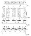
- FIG. 1 represents, very schematically, a flat display screen of the type to which the invention relates.
- This screen includes two plates.
- a first plate 1 commonly called a cathode plate, is disposed opposite a second plate 2 commonly called anode plate.
- These two plates are spaced apart from each other by spacers 3 regularly distributed in the surface of the screen, and a vacuum is formed in the zone delimited by the two plates and a peripheral sealing gasket 4.
- the cathode plate 1 comprises electron generating elements and pixel selection elements (not shown) which can be organized in various ways, for example, as described in US Pat. No. 4,940,916 to US Pat. Atomic Energy in the case of microtip screens.
- the anode plate 2 is, in the case a color screen, provided with alternating bands of phosphor elements, each band corresponding to a color (red, green, blue).
- Figures 2A and 2B show, very schematically, a front view of a portion of an anode plate and a sectional view of this portion.
- the face corresponding to the inner face of the screen is turned upwards.
- the anode comprises, for example, alternating bands 4R, 4G, 4B of phosphor elements respectively red, green and blue.
- the strips of phosphor elements are arranged on corresponding conductive strips 5R, 5G, 5B generally organized into combs, all the 5R bands being connected together as well as all the 5G bands and all the bands. 5B.
- the phosphor elements are divided into elementary patterns, each of which is generally a pixel (in fact, a sub-pixel of each color for a trichromatic screen). These "pixelated" phosphor elements can then always be addressed by polarization electrodes in conductive strips (5G, 5B and 5R) as described in relation to FIGS. 2A and 2B, but a particular mask is used for the deposition of the phosphor elements. .
- the light emitted by the phosphor elements propagates through the anode plate (downwards in Figure 2B).
- the material of the conductive strips 5R, 5G, 5B is then transparent, usually indium tin oxide (ITO).
- the transparent electrodes 5R, 5B, 5G are replaced by opaque and preferably reflecting electrodes, so that as much as possible of the light emitted by the phosphor elements 4R, 4G, 4B is returned to the cathode once these phosphors have been excited by electron bombardment.
- the electron generator plate 1 is then at least partially transparent and the observation takes place through this cathode plate.
- the sets of bands (for example, blue, red, green) are often alternately positively polarized with respect to the cathode 1, so that the electrons extracted from the emitting elements (for example, the microtips) of a pixel of the cathode are alternately directed towards the phosphor elements 4R, 4G, 4B with respect to each of the colors.
- the control in selecting the phosphor to be bombarded by the electrons imposes to control, selectively, the polarization of the phosphor elements of the anode, color by color.
- the bands 5R, 5G, 5B carrying phosphor elements to be excited are biased under a voltage of several hundred volts relative to the cathode, the other bands being at a zero potential.
- the choice of polarization potential values is related to the characteristics of the phosphor elements and the emissive means.
- the anode may, while consisting of several sets of strips of phosphor elements or the like, not be switched per set of bands. All the bands are then polarized at the same potential, at least during the duration of a display frame. This is called an unswitched anode.
- the potential difference between the anode and the cathode is essentially related to the inter-electrode distance, that is to say to the thickness of the internal space.
- a maximum potential difference is sought for reasons of brightness of the screen, which implies that an inter-electrode distance is sought which is as large as possible.
- the structure of the inter-electrode space, which has the spacers 3 may create shadow areas in the screen if they are too large, prevents increasing the inter-electrode distance.
- a resistive layer is provided in the case of microtip screens to receive these microtips and thus limit the formation of destructive short circuits between the microtips and a control grid associated with the cathode.
- arcs may occur not only between the cathode plate and those of the phosphor elements of the anode which are polarized to attract electrons emitted by the microtips, but also between two adjacent bands of phosphor elements. because of the potential difference between these two bands.
- the risk of arcs exists only between anode and cathode.
- interstitial strips 7 of an insulating material (usually silicon oxide).
- these strips are inoperative with respect to the formation of electric arcs between the anode and the cathode.
- the phosphor elements 4R, 4G, 4B significantly exceed the interstitial bands.
- the thickness bands of phosphor elements is generally of the order of about ten ⁇ m and the production of silicon oxide insulation strips of such a thickness is, in practice, incompatible with the technologies used for the manufacture of anodes, so that the thickness of the strips 7 is generally of the order of 1 to 2 ⁇ m , their width being of the order of 10 to 20 ⁇ m .
- a first known solution to try to reduce the appearance of arcs between the anode and the cathode is to provide, at the end of each conductive strip 5R, 5G, 5B, a resistance between the supply line and the strip . As soon as a strong current appears in the band, this resistance causes the voltage to drop. It follows that the potential difference between the conductive strip and the cathode decreases and eliminates the generating voltage of the arc.
- a disadvantage of such a solution is that it does not protect the formation of a lateral electric arc, that is to say between two neighboring bands 5R, 5G, 5B. It may indeed occur a local current flow between two bands which is then not avoided by the end resistors.
- resistors are generally made of ruthenium whose resistivity is stabilized by annealing.
- This annealing at high temperature (of the order of 600 ° C) necessary to stabilize the resistance poses compatibility problems with the screen manufacturing process which requires, in the case where the conductive strips are aluminum in the case of a transparent cathode, temperatures less than 600 °.
- such a method of manufacturing by annealing is difficult to control.
- this solution can give satisfactory results overall, it requires a large space between each band of phosphor elements to accommodate two polarization conductors respectively associated with two neighboring bands while spacing these polarization conductors sufficiently from each other in order to maintain a necessary lateral isolation between them.
- this solution is, in practice, more particularly intended for low resolution screens.
- the anode strips each have a width that is close to but less than 100.
- ⁇ m and the insulating strips 7 have a width of about ten ⁇ m.
- the implementation of a local protection solution resistive layer flanked laterally by polarization bands is not possible because of the small gap between the anode strips.
- the present invention aims at overcoming the drawbacks of conventional techniques by proposing a flat display screen anode which eliminates the risk of the appearance of an electric arc between the anode and the cathode plate, or between two neighboring strips of elements. phosphors of the anode, without impairing the brightness of the screen.
- the present invention also aims at providing a solution that is compatible with the conventional differences between two bands of phosphor elements.
- the present invention also aims at providing a solution that is particularly suitable for a "transparent" cathode screen, that is to say whose cathode plate constitutes the display surface of the screen.
- the invention also aims to propose a solution which respects the conventional manufacturing processes of the anodes and, in particular, the masks used during this manufacture.
- the present invention provides a flat display screen anode, comprising phosphor elements intended to be excited by an electron bombardment, these elements being deposited on at least one polarization electrode constituted, at least to the right of the elements.
- phosphors a stack comprising a resistive layer, itself deposited on a polarization conductive layer of the phosphor elements.
- the phosphor elements are deposited directly on the resistive layer.
- the phosphor elements are deposited on a conductive reflective layer, itself deposited on the resistive layer.
- said reflective layer is deposited in elementary patterns of small dimension in the surface of the anode.
- the phosphor elements are deposited according to the elementary pattern of deposition of the reflective layer.
- the resistive layer is deposited in full plate.
- the resistive layer has the same pattern as the reflective layer.
- the resistive layer has, at least in the active area of the screen, the same pattern as the polarization conductive layer.
- said conductive layer has a pattern of alternate bands interconnected in at least two sets.
- the present invention also provides a flat display screen comprising an electron bombardment cathode of a cathodoluminescent anode.
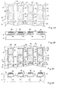
- FIG 3 shows a schematic sectional view of a flat screen anode according to a first embodiment of the present invention.
- This anode comprises, as before, a support plate 2, for example a glass plate. In the case of a monitor observable from the anode, this plate is clearly transparent.
- Anode conductive strips 5R, 5G, 5B are deposited, for example conventionally as illustrated by FIGS. 2A and 2B, and are interconnected by a set of bands assigned to one and the same color.
- a feature of the present invention is that these strips 5R, 5G, 5B are all coated with strips of resistive material 8.
- strips of phosphor elements 4R, 4G, 4B are then deposited on the resistive strips 8 and no longer, as in conventional screens, directly on the conductive strips 5.
- the polarization electrodes of the phosphor elements here consist of a stack of a conductive layer (in which are defined the strips 5R, 5G and 5B) and a resistive layer 8.
- the resistive layer 8 may, in the first embodiment, be deposited, at least in the active part of the screen, that is to say out of the interconnection zones of the sets of strips, with the same pattern as the conductive strips 5R, 5G, 5B anode, so by means of the same mask.
- Another important advantage of the present invention is that, while effectively shielding the screen against destructive electric arcs, the invention does not require any increase in the lateral deviation between the phosphor strips.
- the present invention is therefore particularly suitable for anodes of fine resolution.
- the anode strips 5R, 5G and 5B are preferably separated laterally by insulating interstitial strips 7.
- the invention provides protection against destructive electric arcs not only between the anode plate and the cathode plate, but also between neighboring strips of phosphor elements polarized at different potentials.
- This side protection is particularly effective insofar as it acts against any flow of current, even local.
- the material now accessible is the material of the resistive layer 8, which prevents the formation of destructive electric arcs.
- the choice of the constituent material of the resistive strips 8 depends on the application and, in particular, on the need for transparency (transparent anode) or reflectivity (transparent cathode) of these resistive strips.
- tin oxide or thin silicon, deposited with a thickness of preferably between one and two ⁇ m.
- the conductive strips 5R, 5G, 5B anode are, for example, made of ITO (transparent) or aluminum (reflective) with a thickness of about one tenth of ⁇ m.
- the present invention provides a significant improvement over ruthenium series resistors which must have a thickness of several tens of ⁇ m.
- the first embodiment of the present invention also applies to the case of a monochrome screen in which the anode consists of a plane of phosphor elements of the same color or in the case of a screen (color or monochrome) in which the anode consists of several sets of bands not switched.
- the resistive layer 8 is preferably deposited on the entire conductive anode layer.
- the structure of the phosphor elements of the anode can be very different.
- it may be elementary patterns each of which will correspond to a pixel.
- the present invention provides the additional advantage of being able to be implemented while a solution by lateral protection would take up too much space.
- FIGS. 4A and 4B show, respectively front view and in section, a second embodiment of a flat screen anode according to the invention. This embodiment is more particularly intended for an anode to reflect the light to the cathode plate (1, Figure 1) which then constitutes the surface of the screen.
- a characteristic of the second embodiment of the invention is that the polarization electrodes of the phosphor elements here consist of a stack of three layers.
- an additional conductive layer 10 is deposited on the resistive layer.
- a feature of this additional layer 10 is to be reflective to return light to the cathode.
- the second embodiment makes it possible to use a resistive layer having any optical properties ( transparent, absorbent or reflecting), the optical effect of reflection to the cathode being here ensured by the additional conductive layer 10.
- the second embodiment of the invention applies more particularly to the case where the elements phosphors are deposited by elementary patterns by means of a specific mask comprising apertures, for example, corresponding to the respective sizes of the pixels of the screen or sub-pixels of each color of the screen.
- This characteristic is related to the presence of the conductive layer 10 which must itself be deposited according to these elementary patterns to prevent propagation of charges along the electrode strips.
- the phosphor elements 4'B, 4'R and 4'G are deposited by small surfaces of elementary patterns (in this example, rectangular).
- elementary patterns in this example, rectangular.
- the color distribution of the phosphor elements always takes place in a strip in line with the polarization conducting strips 5B, 5R and 5G which are produced in accordance with FIG. pattern of alternate bands.
- the additional reflective conductive layer is deposited by means of the same mask as the phosphor elements and therefore consists of zones of elementary patterns 10 in line with the phosphor elements.
- An insulating layer 7 is optionally provided between the anode strips. This layer 7 is deposited, as in the first embodiment, on the resistive layer 8 '. However, when it is provided, the insulating layer 7 is then present not only between the anode strips but also between the different elementary patterns of definition of the reflective layer 10 and luminophoric element zones 4. It will be noted that the fact that the additional conductive layer is deposited according to the elementary patterns makes it possible to keep a floating potential at each pixel.
- the resistive layer 8 ' is deposited in full plate, that is to say that it extends at least over the entire active zone of the anode.
- An advantage of the second embodiment of the invention is that it applies particularly well to a screen with transparent cathode. Indeed, by dissociating the functions of reflective layer and resistive layer, there is a greater choice of material to achieve these different layers.
- a resistive layer 8 'of an optically absorbing material for example, silicon.
- the resistive layer will then form an opaque mesh (black matrix) wherever there is neither phosphor nor reflective layer 10. It will then absorb the light, which improves the contrast of the screen.
- the resistive layer if it is deposited full plate, and if it is made of a material with a low secondary emission coefficient (which is generally the case for resistive materials), will protect the underlying layer between the conductive tracks 5B, 5R and 5G which is generally made of a material with a high secondary emission coefficient, and will then protect the anode against charging effects which reduces the degassing of the screen.
- an advantage associated with the suppression of the end resistances of the anode conductive strips is on the one hand that space is gained on the anode but also that one distributes the thermal effects related to the presence of these resistances throughout the anode plate. This avoids localized heating that may be harmful.
- FIGS. 5A and 5B show, respectively front view and in section, an alternative embodiment of an anode according to the second embodiment of the invention.
- the resistive layer 8 " is itself deposited according to the elementary patterns of deposition of the phosphor elements 4 'For the sake of clarity, the differences in alignment between the elementary patterns of the elements have been exaggerated in FIGS. phosphors 4 ', the additional conductive layer 10 and the resistive layer 8 ". It will be noted, however, that these different elementary patterns are obtained by means of the same mask.
- the invention remains perfectly compatible with the processes conventional anodes manufacturing and, in particular, requires no additional mask regardless of the embodiment used.
- the polarization conductive strips 5B, 5R and 5G have again been represented in strips as in the first embodiment.
- the resistive layer provided in the second embodiment of the invention may also be deposited in the pattern of the polarization-conducting strips 5B, 5R and 5G. In this case, we retain the advantage of not using an additional mask for the deposition of this resistive layer as in the first embodiment.
- FIG. 5B illustrates a relatively thicker resistive layer 8 "than that illustrated in FIG. 4B: according to the invention and whatever the embodiment, the value of the resistor can be adjusted as a function of a given material, the thickness of the deposited resistive layer.
- the present invention is susceptible of various variations and modifications which will be apparent to those skilled in the art.
- provision may be made for the polarization conductive layer 5 and that the resistive layer 8 are deposited full plate.
- the reflective conductive layer 10 and the phosphor elements will then be deposited according to the elementary patterns of the pixels of the screen.
- the choice of materials for producing a flat screen anode according to the invention is within the abilities of those skilled in the art from the functional indications given above and applications. Note further that it will be able to adapt the thicknesses of the different layers and in particular the resistive layer according to the expected electrical characteristics.
- the polarization layer 5 may be a conductive plane as the resistive layer may be full plate. There is then only one polarization electrode of the anode.
Landscapes
- Cathode-Ray Tubes And Fluorescent Screens For Display (AREA)
- Devices For Indicating Variable Information By Combining Individual Elements (AREA)
Claims (10)
- Anode für einen flach-ebenen Anzeige- bzw Wiedergabe-Bildschirm, welcher zur Anregung durch ein Elektronenbombardement bestimmte Leuchtstoffelemente (4R, 4G, 4B; 4'R, 4'G, 4'B) aufweist, die auf wenigstens einer Vorspannelektrode abgeschieden sind, dadurch gekennzeichnet daß die genannte Vorspannelektrode wenigstens an den Stellen der Leuchtstoffelemente eine Schichtung aus einer Widerstandsschicht (8, 8', 8"), auf welcher eine Leiterschicht (5B, 5R, 5G) zur Vorspannung der Leuchtstoffelemente abgeschieden ist, aufweist.
- Anode nach Anspruch 1, dadurch gekenn zeichnet, daß die Leuchtstoffelemente (4B, 4R, 4G) direkt auf der Widerstandsschicht (8) abgeschieden sind.
- Anode nach Anspruch 1, dadurch gekennzeichnet, daß die Leuchtstoffelemente (4'B, 4'G, 4'R) auf einer reflektierenden Leiterschicht (10) abgeschieden sind, die ihrerseits auf der Widerstandsschicht (8', 8") abgeschieden ist.
- Anode nach Anspruch 3, dadurch gekennzeichnet, daß die genannte reflektierende Schicht (10) gemäß Elementarmotiven bzw Mustern geringer Abmessung in der Oberfläche der Anode abgeschieden sind.
- Anode nach Anspruch 4, dadurch gekennzeichnet, daß die Leuchtsloffelemente (4'B, 4'R, 4'G) gemäß dem Abscheidungs- Elementarmotiv bzw.-muster der reflektierenden Schicht (10) abgeschieden sind.
- Anode nach einem der Ansprüche 1 bis 5, dadurch gekennzeichnet, daß die Widerstandsschicht (8, 8', 8") ganzflächig abgeschieden ist.
- Anode nach einem der Ansprüche 3 bis 5, dadurch gekennzeichnet, daß die Widerstandsschicht (8") dasselbe Motiv bzw. Muster wie die reflektierende Schicht (10) besitzt.
- Anode nach einem der Ansprüche 1 bis 7, dadurch gekennzeichnet, daß die Widerstandsschicht (8) wenigstens in der aktiven Zone des Bildschirms dasselbe Motiv bzw Muster wie die leitende Vorspannschicht (5) besitzt.
- Anode nach einem der Ansprüche 1 bis 8, dadurch gekennzeichnet, daß die genannte Leiterschicht ein Motiv bzw, eine Musterung abwechselnder Streifen (5R, 5G, 5B), die miteinander in wenigstens zwei Gruppen bzw Ensembles verbunden sind, aufweist.
- Flach-ebener Anzeige- bzw. Wiedergabe- Bildschirm, der eine Kathode (1) zum Elektionenbombardement seitens einer Kathodolumineszenz- Anode (2) gemäß einem der Ansprüche 1 bis 9 besitzt.
Applications Claiming Priority (2)
| Application Number | Priority Date | Filing Date | Title |
|---|---|---|---|
| FR9902654 | 1999-02-26 | ||
| FR9902654A FR2790329B1 (fr) | 1999-02-26 | 1999-02-26 | Anode resistive d'ecran plat de visualisation |
Publications (2)
| Publication Number | Publication Date |
|---|---|
| EP1032017A1 EP1032017A1 (de) | 2000-08-30 |
| EP1032017B1 true EP1032017B1 (de) | 2006-04-26 |
Family
ID=9542780
Family Applications (1)
| Application Number | Title | Priority Date | Filing Date |
|---|---|---|---|
| EP00410018A Expired - Lifetime EP1032017B1 (de) | 1999-02-26 | 2000-02-25 | Anode mit Widerstand für einen flachen Bildschirm |
Country Status (5)
| Country | Link |
|---|---|
| US (1) | US6815885B1 (de) |
| EP (1) | EP1032017B1 (de) |
| JP (1) | JP2000251755A (de) |
| DE (1) | DE60027494T2 (de) |
| FR (1) | FR2790329B1 (de) |
Families Citing this family (4)
| Publication number | Priority date | Publication date | Assignee | Title |
|---|---|---|---|---|
| JP2002164007A (ja) * | 2000-11-24 | 2002-06-07 | Toshiba Corp | 表示装置 |
| JP2006120622A (ja) * | 2004-09-21 | 2006-05-11 | Canon Inc | 発光スクリーン構造及び画像形成装置 |
| JP2009295532A (ja) * | 2008-06-09 | 2009-12-17 | Canon Inc | 発光体基板及びそれを用いた画像表示装置 |
| JP2010015870A (ja) * | 2008-07-04 | 2010-01-21 | Canon Inc | 画像表示装置 |
Family Cites Families (10)
| Publication number | Priority date | Publication date | Assignee | Title |
|---|---|---|---|---|
| DE133615C (de) | ||||
| DD133615A1 (de) * | 1977-11-07 | 1979-01-10 | Hoff Siegfried Von | Anode fuer eine fluoreszenz-anzeigeroehre |
| JPS609039A (ja) * | 1983-06-28 | 1985-01-18 | Ise Electronics Corp | 螢光表示管 |
| JPH0326617Y2 (de) * | 1984-09-17 | 1991-06-10 | ||
| JPS62126528A (ja) * | 1985-11-26 | 1987-06-08 | Ise Electronics Corp | 螢光表示管 |
| KR950034365A (ko) * | 1994-05-24 | 1995-12-28 | 윌리엄 이. 힐러 | 평판 디스플레이의 애노드 플레이트 및 이의 제조 방법 |
| FR2732160B1 (fr) * | 1995-03-22 | 1997-06-13 | Pixtech Sa | Anode d'ecran plat de visualisation a bandes resistives |
| JP3066573B2 (ja) * | 1996-10-30 | 2000-07-17 | 双葉電子工業株式会社 | 電界放出型表示素子 |
| FR2756969B1 (fr) * | 1996-12-06 | 1999-01-08 | Commissariat Energie Atomique | Ecran d'affichage comprenant une source d'electrons a micropointes, observable a travers le support des micropointes, et procede de fabrication de cette source |
| JPH11185674A (ja) * | 1997-12-24 | 1999-07-09 | Futaba Corp | 表示管用陽極基板とその製造方法 |
-
1999
- 1999-02-26 FR FR9902654A patent/FR2790329B1/fr not_active Expired - Fee Related
-
2000
- 2000-02-17 JP JP2000039882A patent/JP2000251755A/ja not_active Withdrawn
- 2000-02-23 US US09/511,203 patent/US6815885B1/en not_active Expired - Fee Related
- 2000-02-25 DE DE60027494T patent/DE60027494T2/de not_active Expired - Fee Related
- 2000-02-25 EP EP00410018A patent/EP1032017B1/de not_active Expired - Lifetime
Also Published As
| Publication number | Publication date |
|---|---|
| DE60027494D1 (de) | 2006-06-01 |
| DE60027494T2 (de) | 2007-04-19 |
| FR2790329B1 (fr) | 2001-05-18 |
| JP2000251755A (ja) | 2000-09-14 |
| EP1032017A1 (de) | 2000-08-30 |
| FR2790329A1 (fr) | 2000-09-01 |
| US6815885B1 (en) | 2004-11-09 |
Similar Documents
| Publication | Publication Date | Title |
|---|---|---|
| EP0704877A1 (de) | Elektrischer Schutz von einer Anode eines flachen Bildschirms | |
| FR2679057A1 (fr) | Structure d'ecran a cristal liquide, a matrice active et a haute definition. | |
| EP1139374A1 (de) | Kathodenplatte für einen flachen Bildschirm | |
| FR2761523A1 (fr) | Pose d'espaceurs dans un ecran plat de visualisation | |
| EP1032017B1 (de) | Anode mit Widerstand für einen flachen Bildschirm | |
| EP0734042B1 (de) | Anode eines flachen Bildschirms mit Widerstandsstreifen | |
| EP0724771B1 (de) | Flacher bildschirm mit hoher spannung zwischen elektroden | |
| EP0806788A1 (de) | Anode eines flachen Bildschirms mit Schutzring | |
| EP0877407A1 (de) | Anode eines flachen Bildschirms | |
| EP0732723B1 (de) | Flaches Bildschirm mit hohem Inter-Elektrodenabstand | |
| EP1096542A1 (de) | Flasches Bildschirm mit Schutzgitter | |
| EP0649162B1 (de) | Flaches Kaltkathodeanzeigegerät mit geschalteter Anode | |
| EP0844642A1 (de) | Flaches Bildschirm mit fokussierenden Gittern | |
| EP0806787B1 (de) | Herstellung einer Anode eines flachen Bildschirms | |
| EP0844643A1 (de) | Flaches Bildschirm mit seitlicher Ablenkung | |
| EP0867908A1 (de) | Vergleichmässigung der potentiellen Elektronenemission einer Kathode eines flachen Mikrospitzen-Bildschirms | |
| EP0911858A1 (de) | Entfernung des moire-effekts eines flachen bildschirms | |
| EP0806790B1 (de) | Mikrospitzen-Farbbildschirm mit zwei Gittern | |
| EP0948026A1 (de) | Leitende Durchführung durch eine Dichtungswand eines flachen Bildschirms | |
| EP0905670A1 (de) | Vereinfachung einer Mikrospitzen-Anzeige mit einer Rücksetzungselektrode | |
| WO2000021112A1 (fr) | Source d'electrons comportant au moins une electrode de protection contre des emissions parasites | |
| FR2828956A1 (fr) | Protection locale d'une grille d'ecran plat a micropointes | |
| FR2859811A1 (fr) | Panneau electroluminescent d'eclairage ou de visualisation d'images dote d'electrodes superieures transparentes renforcees par des grilles | |
| FR2797092A1 (fr) | Procede de fabrication d'une anode d'un ecran plat de visualisation | |
| FR2800511A1 (fr) | Ecran plat de visualisation a grille de protection |
Legal Events
| Date | Code | Title | Description |
|---|---|---|---|
| PUAI | Public reference made under article 153(3) epc to a published international application that has entered the european phase |
Free format text: ORIGINAL CODE: 0009012 |
|
| AK | Designated contracting states |
Kind code of ref document: A1 Designated state(s): DE FR GB IT |
|
| AX | Request for extension of the european patent |
Free format text: AL;LT;LV;MK;RO;SI |
|
| 17P | Request for examination filed |
Effective date: 20010214 |
|
| AKX | Designation fees paid |
Free format text: DE FR GB IT |
|
| 19U | Interruption of proceedings before grant |
Effective date: 20020621 |
|
| 19W | Proceedings resumed before grant after interruption of proceedings |
Effective date: 20050502 |
|
| RAP1 | Party data changed (applicant data changed or rights of an application transferred) |
Owner name: LE COMMISSARIAT AE L'ENERGIE ATOMIQUE |
|
| GRAP | Despatch of communication of intention to grant a patent |
Free format text: ORIGINAL CODE: EPIDOSNIGR1 |
|
| GRAS | Grant fee paid |
Free format text: ORIGINAL CODE: EPIDOSNIGR3 |
|
| RAP1 | Party data changed (applicant data changed or rights of an application transferred) |
Owner name: COMMISSARIAT A L'ENERGIE ATOMIQUE |
|
| GRAA | (expected) grant |
Free format text: ORIGINAL CODE: 0009210 |
|
| AK | Designated contracting states |
Kind code of ref document: B1 Designated state(s): DE FR GB IT |
|
| PG25 | Lapsed in a contracting state [announced via postgrant information from national office to epo] |
Ref country code: IT Free format text: LAPSE BECAUSE OF FAILURE TO SUBMIT A TRANSLATION OF THE DESCRIPTION OR TO PAY THE FEE WITHIN THE PRE;WARNING: LAPSES OF ITALIAN PATENTS WITH EFFECTIVE DATE BEFORE 2007 MAY HAVE OCCURRED AT ANY TIME BEFORE 2007. THE CORRECT EFFECTIVE DATE MAY BE DIFFERENT FROM THE ONE RECORDED.SCRIBED TIME-LIMIT Effective date: 20060426 |
|
| REG | Reference to a national code |
Ref country code: GB Ref legal event code: FG4D Free format text: NOT ENGLISH |
|
| REF | Corresponds to: |
Ref document number: 60027494 Country of ref document: DE Date of ref document: 20060601 Kind code of ref document: P |
|
| GBT | Gb: translation of ep patent filed (gb section 77(6)(a)/1977) | ||
| PGFP | Annual fee paid to national office [announced via postgrant information from national office to epo] |
Ref country code: GB Payment date: 20070119 Year of fee payment: 8 |
|
| PGFP | Annual fee paid to national office [announced via postgrant information from national office to epo] |
Ref country code: DE Payment date: 20070222 Year of fee payment: 8 |
|
| PLBE | No opposition filed within time limit |
Free format text: ORIGINAL CODE: 0009261 |
|
| STAA | Information on the status of an ep patent application or granted ep patent |
Free format text: STATUS: NO OPPOSITION FILED WITHIN TIME LIMIT |
|
| 26N | No opposition filed |
Effective date: 20070129 |
|
| PGFP | Annual fee paid to national office [announced via postgrant information from national office to epo] |
Ref country code: IT Payment date: 20070622 Year of fee payment: 8 |
|
| PGFP | Annual fee paid to national office [announced via postgrant information from national office to epo] |
Ref country code: FR Payment date: 20070228 Year of fee payment: 8 |
|
| GBPC | Gb: european patent ceased through non-payment of renewal fee |
Effective date: 20080225 |
|
| REG | Reference to a national code |
Ref country code: FR Ref legal event code: ST Effective date: 20081031 |
|
| PG25 | Lapsed in a contracting state [announced via postgrant information from national office to epo] |
Ref country code: DE Free format text: LAPSE BECAUSE OF NON-PAYMENT OF DUE FEES Effective date: 20080902 |
|
| PG25 | Lapsed in a contracting state [announced via postgrant information from national office to epo] |
Ref country code: FR Free format text: LAPSE BECAUSE OF NON-PAYMENT OF DUE FEES Effective date: 20080229 |
|
| PG25 | Lapsed in a contracting state [announced via postgrant information from national office to epo] |
Ref country code: GB Free format text: LAPSE BECAUSE OF NON-PAYMENT OF DUE FEES Effective date: 20080225 |
|
| PG25 | Lapsed in a contracting state [announced via postgrant information from national office to epo] |
Ref country code: IT Free format text: LAPSE BECAUSE OF NON-PAYMENT OF DUE FEES Effective date: 20080225 |