EP1032031A2 - Monolithisch auf einem Halbleiter integriertes elektronisches Leistungsbauelement mit Strukturen zum Schutz der Ecken mit begrenzter Flächengrösse - Google Patents
Monolithisch auf einem Halbleiter integriertes elektronisches Leistungsbauelement mit Strukturen zum Schutz der Ecken mit begrenzter Flächengrösse Download PDFInfo
- Publication number
- EP1032031A2 EP1032031A2 EP99830532A EP99830532A EP1032031A2 EP 1032031 A2 EP1032031 A2 EP 1032031A2 EP 99830532 A EP99830532 A EP 99830532A EP 99830532 A EP99830532 A EP 99830532A EP 1032031 A2 EP1032031 A2 EP 1032031A2
- Authority
- EP
- European Patent Office
- Prior art keywords
- trench
- semiconductor
- junction
- region
- electronic device
- Prior art date
- Legal status (The legal status is an assumption and is not a legal conclusion. Google has not performed a legal analysis and makes no representation as to the accuracy of the status listed.)
- Granted
Links
Images


Classifications
-
- H—ELECTRICITY
- H10—SEMICONDUCTOR DEVICES; ELECTRIC SOLID-STATE DEVICES NOT OTHERWISE PROVIDED FOR
- H10D—INORGANIC ELECTRIC SEMICONDUCTOR DEVICES
- H10D62/00—Semiconductor bodies, or regions thereof, of devices having potential barriers
- H10D62/10—Shapes, relative sizes or dispositions of the regions of the semiconductor bodies; Shapes of the semiconductor bodies
- H10D62/113—Isolations within a component, i.e. internal isolations
- H10D62/115—Dielectric isolations, e.g. air gaps
- H10D62/116—Dielectric isolations, e.g. air gaps adjoining the input or output regions of field-effect devices, e.g. adjoining source or drain regions
-
- H—ELECTRICITY
- H10—SEMICONDUCTOR DEVICES; ELECTRIC SOLID-STATE DEVICES NOT OTHERWISE PROVIDED FOR
- H10D—INORGANIC ELECTRIC SEMICONDUCTOR DEVICES
- H10D62/00—Semiconductor bodies, or regions thereof, of devices having potential barriers
- H10D62/10—Shapes, relative sizes or dispositions of the regions of the semiconductor bodies; Shapes of the semiconductor bodies
- H10D62/102—Constructional design considerations for preventing surface leakage or controlling electric field concentration
- H10D62/103—Constructional design considerations for preventing surface leakage or controlling electric field concentration for increasing or controlling the breakdown voltage of reverse-biased devices
- H10D62/104—Constructional design considerations for preventing surface leakage or controlling electric field concentration for increasing or controlling the breakdown voltage of reverse-biased devices having particular shapes of the bodies at or near reverse-biased junctions, e.g. having bevels or moats
-
- H—ELECTRICITY
- H10—SEMICONDUCTOR DEVICES; ELECTRIC SOLID-STATE DEVICES NOT OTHERWISE PROVIDED FOR
- H10D—INORGANIC ELECTRIC SEMICONDUCTOR DEVICES
- H10D84/00—Integrated devices formed in or on semiconductor substrates that comprise only semiconducting layers, e.g. on Si wafers or on GaAs-on-Si wafers
-
- H—ELECTRICITY
- H10—SEMICONDUCTOR DEVICES; ELECTRIC SOLID-STATE DEVICES NOT OTHERWISE PROVIDED FOR
- H10W—GENERIC PACKAGES, INTERCONNECTIONS, CONNECTORS OR OTHER CONSTRUCTIONAL DETAILS OF DEVICES COVERED BY CLASS H10
- H10W10/00—Isolation regions in semiconductor bodies between components of integrated devices
- H10W10/01—Manufacture or treatment
- H10W10/011—Manufacture or treatment of isolation regions comprising dielectric materials
- H10W10/012—Manufacture or treatment of isolation regions comprising dielectric materials using local oxidation of silicon [LOCOS]
- H10W10/0121—Manufacture or treatment of isolation regions comprising dielectric materials using local oxidation of silicon [LOCOS] in regions recessed from the surface, e.g. in trenches or grooves
- H10W10/0123—Manufacture or treatment of isolation regions comprising dielectric materials using local oxidation of silicon [LOCOS] in regions recessed from the surface, e.g. in trenches or grooves using auxiliary pillars in the regions
-
- H—ELECTRICITY
- H10—SEMICONDUCTOR DEVICES; ELECTRIC SOLID-STATE DEVICES NOT OTHERWISE PROVIDED FOR
- H10W—GENERIC PACKAGES, INTERCONNECTIONS, CONNECTORS OR OTHER CONSTRUCTIONAL DETAILS OF DEVICES COVERED BY CLASS H10
- H10W10/00—Isolation regions in semiconductor bodies between components of integrated devices
- H10W10/01—Manufacture or treatment
- H10W10/031—Manufacture or treatment of isolation regions comprising PN junctions
-
- H—ELECTRICITY
- H10—SEMICONDUCTOR DEVICES; ELECTRIC SOLID-STATE DEVICES NOT OTHERWISE PROVIDED FOR
- H10W—GENERIC PACKAGES, INTERCONNECTIONS, CONNECTORS OR OTHER CONSTRUCTIONAL DETAILS OF DEVICES COVERED BY CLASS H10
- H10W10/00—Isolation regions in semiconductor bodies between components of integrated devices
- H10W10/10—Isolation regions comprising dielectric materials
- H10W10/13—Isolation regions comprising dielectric materials formed using local oxidation of silicon [LOCOS], e.g. sealed interface localised oxidation [SILO] or side-wall mask isolation [SWAMI]
-
- H—ELECTRICITY
- H10—SEMICONDUCTOR DEVICES; ELECTRIC SOLID-STATE DEVICES NOT OTHERWISE PROVIDED FOR
- H10W—GENERIC PACKAGES, INTERCONNECTIONS, CONNECTORS OR OTHER CONSTRUCTIONAL DETAILS OF DEVICES COVERED BY CLASS H10
- H10W10/00—Isolation regions in semiconductor bodies between components of integrated devices
- H10W10/30—Isolation regions comprising PN junctions
Definitions
- This invention relates to an electronic power device monolithically integrated on a semiconductor substrate and having edge protection structures of limited planar size.
- the invention specifically relates to a monolithic semiconductor device wherein P/N junctions are capable of sustaining high operating voltages, a base-collector junction of an NPN bipolar transistor being exemplary of these.
- the invention further relates to a method of manufacturing the protection structure of limited planar size.
- the invention relates, particularly but not exclusively, to a structure of limited planar size which functions as an edge structure for a VIPOWER type of power device, and the description to follow will make reference to this field of application for convenience of illustration only.
- most of the P/N junctions fabricated with planar technology comprise basically a first semiconductor region having a first type of conductivity and being diffused into a second semiconductor region with the opposite type of conductivity from the first.
- An insulating layer of silicon oxide is laid over both regions, and metal contacts are then formed to establish an electric connection to the two semiconductor regions.
- a depleted region is associated with the P/N junction.
- This depleted region can be regarded as formed of two regions: a first region along a planar region of the junction, and the second region at the edges of the planar region.
- the equipotential lines lie parallel to the junction, the peak electric field is centered at the junction, and the field breakdown occurs upon the field reaching its critical value.
- the equipotential lines curve and are more crowded together at the junction edges than in the planar region, due to the junction depth being finite. Consequently, the electric field at the edge region is increased; stronger electric fields being associated with smaller radii of curvature.
- the breakdown voltage of a finite P/N junction is usually lower than that associated with the corresponding planar junction because of the electric field being much stronger at the edge region.
- the breakdown voltage ratio between the edge and the planar portion is, therefore, smaller than unity.
- a first prior approach to filling this demand provided for the use of metal field plates located proximate to the structure edge.
- the field plates are not in direct contact with the silicon surface, but rest on the previously deposited, or grown, layer of silicon oxide.
- a major feature of metal layers immersed in an electric field is that they set at a single potential throughout their spread. Accordingly, the metal field plates, if suitably dimensioned, will force the depleted region to span a large area, thus preventing crowding of the equipotential lines.
- this first of the prior approaches has certain drawbacks.
- the surface electric field still remains high, and even if below the critical value, may be sensitive to the amount of surface charge brought about by the presence of moving charges or fixed charges at the oxide/silicon interface, introduced during the process steps for manufacturing the power devices.
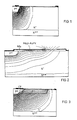
- a second prior approach disclosed in GB-A-216597, proposes high-resistivity rings placed in electric contact with the main junction to be protected. Referring to Figure 3, this approach, by forcing the depleted region to span broader regions, also results in thinned equipotential lines and, hence, a weaker surface electric field.
- the technical problem underlying this invention is to provide a device for high-voltage operation with protection structures effective to combine proper performance of the device through its operational range with reduced planar size, thereby overcoming the drawbacks of devices according to the prior art.
- the concept behind the present invention is that of providing an electronic power device with a protective structure of limited planar size by using trench structures of substantial thickness formed within the silicon substrate and completely filled with dielectric material.
- the presence of a trench in direct contact with the P/N junction is effective, in a reverse bias situation, to cause the equipotential lines to crowd together within the trench-filling dielectric material.
- the oxide-filled trench structure can be made much smaller than edge structures according to the prior art.
- a conventional edge structure for a power device which is to sustain a reverse bias voltage of 700V would account for approximately 40% of the device total area, whereas an edge structure according to this invention would be a planar size equal to about 10-15% of the device total area.
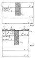
- An epitaxial layer 2 of the N - type is grown over the surface of an N + substrate 1.
- a region 3 of the P type, buried relative to the final surface of the device, is diffused into the epitaxial layer 2. Again by diffusion, a region 4 of the N + type is formed within the region 3 which will also be buried relative to the final surface of the device.
- a second epitaxial layer 5 of the N - type is grown over the surface of the epitaxial layer 2.
- the substrate 1 constitutes, with the epitaxial layer 2 and the epitaxial layer 5, the bulk region of the transistor.
- a thin oxide layer 6 is formed over the surface of the epitaxial layer, e.g. to a thickness of a few hundred ⁇ ngstrom.
- a layer 7 of a dielectric material specifically silicon nitride, e.g. to a thickness of about one thousand ⁇ ngstrom.
- a thick edge protection structure having a silicon oxide trench of suitable dimensions to sustain operating voltages of up to 700V.
- the trench is 30 ⁇ m deep and 30 ⁇ m wide.
- a plurality of small equispaced trenches 8 are formed in the layers 5 and 2, within the region where this protection structure is to be provided, as shown in Figure 6, using conventional photolithographic techniques and successive etching processes through the layers 7 and 6, the epitaxial layer 5, and a portion of the epitaxial layer 2.
- the small equispaced trenches 8 are parallel to one another.
- the regions of the small equispaced trenches 8 bound a plurality of walls 9 of semiconductor material.
- These walls 9 extend parallel to the small equispaced trenches 8 and exhibit an essentially comb-like profile when viewed in a vertical cross-section through at least two walls 9.
- the nitride layer 7 is then removed from the structure, and the semiconductor is subjected to a thermal treatment in an oxidising medium.
- the oxidising thermal treatment should be adequate to turn all the silicon walls that delimit the trenches into oxide.
- a dielectric layer with planarizing properties can be deposited to fill the vacant trench regions.
- these small equispaced trenches 8 are arranged to interrupt the buried region 3 of the P type, thereby providing a junction of the "mesa" type. In this way, the finished trench 10 will suppress the spiking effect.
- this advantageous embodiment can only be implemented with a finished trench 10 which has been obtained from the plural small equispaced trenches 8 according to this invention, and is impracticable with a single trench obtained by filling in as in the prior art.
- An anisotropic planarizing etch-back is then carried out which may be followed by a planarizing process, e.g. of a chemio-mechanical nature.
- the top surface of the oxide-filled trench 10 and the surface of the layer 5 are coplanar, thus allowing the process flow for forming the power device to be carried out conventionally.
- a region 11 of the P + type is formed by diffusion at the left-hand side of the oxide-filled trench which constitutes, in combination with the region 3, the base region of the NPN transistor. Furthermore, the region 11 locally improves the transistor base region such that the electric field can be reduced locally.
- this region 11 need not be in contact with the trench 10 for the device to perform correctly.
- this region 11 is not even strictly necessary; it has been introduced to establish a contact to the buried region P, and may be omitted where this contact is not required.
- the region 12 constitutes the emitter of the NPN transistor, and the region 13 constitutes the channel stopper.
- the whole surface area is then covered with an insulating oxide 14, wherewithin contact areas are formed to enable the metal strips 15, 16, 17 to contact the regions 18, 19, 20, respectively.
- the metallization layer 16 will not cover the trench 10, since it is not required to function as a field plate for straightening the field lines inside the junction.
- the metallization layer 17 extends to a distance short of the trench 10 which is dependent on the voltage sustaining specifications for the device.
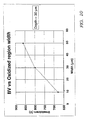
- Figures 9 and 10 illustrate graphically the dependence of the breakdown voltage of the junction on the varying depth ( Figure 9) and breadth ( Figure 10) of the trench structure.
Landscapes
- Semiconductor Integrated Circuits (AREA)
Priority Applications (2)
| Application Number | Priority Date | Filing Date | Title |
|---|---|---|---|
| EP99830532A EP1032031B1 (de) | 1998-10-23 | 1999-08-26 | Monolithisch auf einem Halbleiter integriertes elektronisches Leistungsbauelement mit Strukturen zum Schutz der Ecken mit begrenzter Flächengrösse und zugehöriges Herstellungsverfahren |
| US09/613,108 US6495423B1 (en) | 1999-08-26 | 2000-07-10 | Electronic power device monolithically integrated on a semiconductor and comprising edge protection structures having a limited planar dimension |
Applications Claiming Priority (3)
| Application Number | Priority Date | Filing Date | Title |
|---|---|---|---|
| EP98830638 | 1998-10-23 | ||
| EP98830638A EP0996158B9 (de) | 1998-10-23 | 1998-10-23 | Auf einem Halbleitersubstrat integrierte Hochspannungs-Widerstandsstruktur |
| EP99830532A EP1032031B1 (de) | 1998-10-23 | 1999-08-26 | Monolithisch auf einem Halbleiter integriertes elektronisches Leistungsbauelement mit Strukturen zum Schutz der Ecken mit begrenzter Flächengrösse und zugehöriges Herstellungsverfahren |
Publications (3)
| Publication Number | Publication Date |
|---|---|
| EP1032031A2 true EP1032031A2 (de) | 2000-08-30 |
| EP1032031A3 EP1032031A3 (de) | 2001-03-14 |
| EP1032031B1 EP1032031B1 (de) | 2007-10-10 |
Family
ID=26152178
Family Applications (1)
| Application Number | Title | Priority Date | Filing Date |
|---|---|---|---|
| EP99830532A Expired - Lifetime EP1032031B1 (de) | 1998-10-23 | 1999-08-26 | Monolithisch auf einem Halbleiter integriertes elektronisches Leistungsbauelement mit Strukturen zum Schutz der Ecken mit begrenzter Flächengrösse und zugehöriges Herstellungsverfahren |
Country Status (1)
| Country | Link |
|---|---|
| EP (1) | EP1032031B1 (de) |
Cited By (1)
| Publication number | Priority date | Publication date | Assignee | Title |
|---|---|---|---|---|
| JP7712730B1 (ja) * | 2024-12-31 | 2025-07-24 | ATI Japan 株式会社 | 酸化シリコン膜をもつシリコン基板の製造方法 |
Family Cites Families (7)
| Publication number | Priority date | Publication date | Assignee | Title |
|---|---|---|---|---|
| JPS58161342A (ja) * | 1982-03-18 | 1983-09-24 | Seiko Instr & Electronics Ltd | 半導体装置の製造方法 |
| JPS59112633A (ja) * | 1982-12-18 | 1984-06-29 | Toshiba Corp | 半導体装置 |
| IT1215024B (it) * | 1986-10-01 | 1990-01-31 | Sgs Microelettronica Spa | Processo per la formazione di un dispositivo monolitico a semiconduttore di alta tensione |
| US5308786A (en) * | 1993-09-27 | 1994-05-03 | United Microelectronics Corporation | Trench isolation for both large and small areas by means of silicon nodules after metal etching |
| JP3252569B2 (ja) * | 1993-11-09 | 2002-02-04 | 株式会社デンソー | 絶縁分離基板及びそれを用いた半導体装置及びその製造方法 |
| US5374583A (en) * | 1994-05-24 | 1994-12-20 | United Microelectronic Corporation | Technology for local oxidation of silicon |
| DE69533773D1 (de) * | 1995-03-31 | 2004-12-23 | Cons Ric Microelettronica | Verfahren zur Herstellung von Isolationsgraben |
-
1999
- 1999-08-26 EP EP99830532A patent/EP1032031B1/de not_active Expired - Lifetime
Cited By (1)
| Publication number | Priority date | Publication date | Assignee | Title |
|---|---|---|---|---|
| JP7712730B1 (ja) * | 2024-12-31 | 2025-07-24 | ATI Japan 株式会社 | 酸化シリコン膜をもつシリコン基板の製造方法 |
Also Published As
| Publication number | Publication date |
|---|---|
| EP1032031A3 (de) | 2001-03-14 |
| EP1032031B1 (de) | 2007-10-10 |
Similar Documents
| Publication | Publication Date | Title |
|---|---|---|
| US5648283A (en) | High density power device fabrication process using undercut oxide sidewalls | |
| US7696571B2 (en) | Method of manufacturing a trench transistor having a heavy body region | |
| US5387528A (en) | Method of manufacturing a semiconductor device comprising an insulated gate field effect device | |
| KR100816253B1 (ko) | 트렌치 게이트 전계 효과 트랜지스터 및 그의 제조 방법 | |
| EP1415334B1 (de) | Herstellung von halbleiteranordnungen mit schottky sperrschichten | |
| KR101336534B1 (ko) | 반도체 디바이스 및 그 형성 방법 | |
| EP1290735B1 (de) | Halbleiterbauelement | |
| WO2001057915A2 (en) | Trenched schottky rectifiers | |
| EP2118933A1 (de) | Halbleiterbauelement und verfahren zur herstellung eines halbleiterbauelements | |
| US8017494B2 (en) | Termination trench structure for mosgated device and process for its manufacture | |
| US20040018705A1 (en) | Semiconductor structure and method for processing such a structure | |
| US6133606A (en) | High voltage complementary semiconductor device (HV-CMOS) with gradient doping electrodes | |
| EP1032031A2 (de) | Monolithisch auf einem Halbleiter integriertes elektronisches Leistungsbauelement mit Strukturen zum Schutz der Ecken mit begrenzter Flächengrösse | |
| US6495423B1 (en) | Electronic power device monolithically integrated on a semiconductor and comprising edge protection structures having a limited planar dimension | |
| US6693019B2 (en) | Method of manufacturing an electronic power device monolithically integrated on a semiconductor and comprising a first power region, a second region, and an isolation structure of limited planar dimension | |
| US20040018704A1 (en) | Multirate circular buffer and method of operating the same | |
| EP1037274A2 (de) | Auf einem Halbleiter integriertes elektronisches Leistungsbauelement mit einem ersten Bereich für das Leistungsbauelement und mindestens einem zweiten Bereich und einer Isolationsstruktur mit begrenzter Flächengrösse | |
| US5184201A (en) | Static induction transistor |
Legal Events
| Date | Code | Title | Description |
|---|---|---|---|
| PUAI | Public reference made under article 153(3) epc to a published international application that has entered the european phase |
Free format text: ORIGINAL CODE: 0009012 |
|
| AK | Designated contracting states |
Kind code of ref document: A2 Designated state(s): DE FR GB IT |
|
| AX | Request for extension of the european patent |
Free format text: AL;LT;LV;MK;RO;SI |
|
| PUAL | Search report despatched |
Free format text: ORIGINAL CODE: 0009013 |
|
| AK | Designated contracting states |
Kind code of ref document: A3 Designated state(s): AT BE CH CY DE DK ES FI FR GB GR IE IT LI LU MC NL PT SE |
|
| AX | Request for extension of the european patent |
Free format text: AL;LT;LV;MK;RO;SI |
|
| RIC1 | Information provided on ipc code assigned before grant |
Free format text: 7H 01L 21/762 A, 7H 01L 27/06 B, 7H 01L 21/761 B |
|
| 17P | Request for examination filed |
Effective date: 20010628 |
|
| AKX | Designation fees paid |
Free format text: DE FR GB IT |
|
| GRAP | Despatch of communication of intention to grant a patent |
Free format text: ORIGINAL CODE: EPIDOSNIGR1 |
|
| RTI1 | Title (correction) |
Free format text: ELECTRONIC POWER DEVICE MONOLITHICALLY INTEGRATED ON A SEMICONDUCTOR AND COMPRISING EDGE PROTECTION STRUCTURES HAVING A LIMITED PLANAR DIMENSION AND ITS MANUFACTURING METHOD |
|
| GRAS | Grant fee paid |
Free format text: ORIGINAL CODE: EPIDOSNIGR3 |
|
| GRAA | (expected) grant |
Free format text: ORIGINAL CODE: 0009210 |
|
| AK | Designated contracting states |
Kind code of ref document: B1 Designated state(s): DE FR GB IT |
|
| REG | Reference to a national code |
Ref country code: GB Ref legal event code: FG4D |
|
| REF | Corresponds to: |
Ref document number: 69937285 Country of ref document: DE Date of ref document: 20071122 Kind code of ref document: P |
|
| EN | Fr: translation not filed | ||
| PLBE | No opposition filed within time limit |
Free format text: ORIGINAL CODE: 0009261 |
|
| STAA | Information on the status of an ep patent application or granted ep patent |
Free format text: STATUS: NO OPPOSITION FILED WITHIN TIME LIMIT |
|
| 26N | No opposition filed |
Effective date: 20080711 |
|
| PG25 | Lapsed in a contracting state [announced via postgrant information from national office to epo] |
Ref country code: FR Free format text: LAPSE BECAUSE OF FAILURE TO SUBMIT A TRANSLATION OF THE DESCRIPTION OR TO PAY THE FEE WITHIN THE PRESCRIBED TIME-LIMIT Effective date: 20080725 Ref country code: DE Free format text: LAPSE BECAUSE OF FAILURE TO SUBMIT A TRANSLATION OF THE DESCRIPTION OR TO PAY THE FEE WITHIN THE PRESCRIBED TIME-LIMIT Effective date: 20080111 |
|
| GBPC | Gb: european patent ceased through non-payment of renewal fee |
Effective date: 20080826 |
|
| PG25 | Lapsed in a contracting state [announced via postgrant information from national office to epo] |
Ref country code: IT Free format text: LAPSE BECAUSE OF NON-PAYMENT OF DUE FEES Effective date: 20080826 |
|
| PG25 | Lapsed in a contracting state [announced via postgrant information from national office to epo] |
Ref country code: GB Free format text: LAPSE BECAUSE OF NON-PAYMENT OF DUE FEES Effective date: 20080826 |