EP1032071B1 - Breitbandige Symmetrierschaltung für drahtlose und hochfrequente Anwendungen - Google Patents
Breitbandige Symmetrierschaltung für drahtlose und hochfrequente Anwendungen Download PDFInfo
- Publication number
- EP1032071B1 EP1032071B1 EP00301171A EP00301171A EP1032071B1 EP 1032071 B1 EP1032071 B1 EP 1032071B1 EP 00301171 A EP00301171 A EP 00301171A EP 00301171 A EP00301171 A EP 00301171A EP 1032071 B1 EP1032071 B1 EP 1032071B1
- Authority
- EP
- European Patent Office
- Prior art keywords
- transmission line
- balun transformer
- line elements
- signal coupler
- pairs
- Prior art date
- Legal status (The legal status is an assumption and is not a legal conclusion. Google has not performed a legal analysis and makes no representation as to the accuracy of the status listed.)
- Expired - Lifetime
Links
Images



Classifications
-
- H—ELECTRICITY
- H01—ELECTRIC ELEMENTS
- H01P—WAVEGUIDES; RESONATORS, LINES, OR OTHER DEVICES OF THE WAVEGUIDE TYPE
- H01P5/00—Coupling devices of the waveguide type
- H01P5/08—Coupling devices of the waveguide type for linking dissimilar lines or devices
- H01P5/10—Coupling devices of the waveguide type for linking dissimilar lines or devices for coupling balanced lines or devices with unbalanced lines or devices
Definitions
- the present invention is directed to a balun transformer for providing a single ended output signal from a pair of differential input signals, and more particularly to a transmission line balun implemented by a pair of inter-coupled transmission line signal couplers.
- RF wireless circuits utilize balanced outputs of signals to minimize the effect of ground inductance and to improve common mode rejection.
- Such circuitry include mixers, modulators, IF strips and voltage controlled oscillators.
- These balanced outputs moreover, consist of differential signals which must be combined to provide a single ended output signal.
- One known type of device for combining differential signals into a single ended output signal is referred to in the art as a "balun" (balanced input/unbalanced output).
- baluns are tightly coupled structures fabricated much like a conventional transformer utilizing discrete components; however, the turns are arranged physically to include the interwinding capacitances as components of the characteristic impedance of a transmission line.
- baluns have been implemented using distributed components. See, for example, GB-A-2 311 417 . When implemented with discrete components, they add excessive loss and increase the cost of fabrication. When implemented in distributed form they exhibit less loss, but at wireless frequencies require a relatively large amount of board space together with an inherent limitation of being narrow band devices.
- the present invention is directed to an improvement in apparatus for implementing a transmission line balun transformer for providing a single ended output signal from a pair of differential input signals. This is achieved by cross coupling the components of a pair of transmission line signal couplers in tandem. At least one of the couplers is designed to be a relatively loosely coupled device, typically having a coupling characteristic, i.e., coupling factor greater than 3dB. When desirable, both couplers can have the same or unequal coupling factor. However, the two couplers are coupled together with proper phase relationships so as to achieve a relatively tighter resulting coupling characteristic, preferably about 3dB, thereby resulting in an increase in bandwidth.
- each coupler comprises a microstrip transmission line coupler including pairs of mutually adjacent microstrip transmission line elements formed on opposite sides of a dielectric support member, such as a circuit board, and also including an intermediate ground plane for mutually isolating the couplers.
- the couplers are internally coupled together through apertures in the ground plane, with the pair of input signal ports and an output port being located on one outer edge surface of the printed circuit board.
- the transmission line elements can be elongated microstrips of constant width, in the form of a sawtooth or wiggly elements, and can be tapered either in width or separation.
- the coupler can be fabricated as a stripline device.
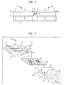
- FIG. 1 shown thereat is an electrical schematic diagram of a first embodiment of the invention which comprises two relatively loosely coupled transmission line couplers C 1 and C 2 .
- the couplers are implemented by pairs of mutually parallel microstrip transmission line elements a 1 , a 2 , and b 1 , b 2 of substantially equal length.
- the input ends of these elements are designated by reference numerals 1, 3, 5 and 7, while the output ends thereof are designated by reference numerals 2, 4, 6, and 8, as shown.
- the coupler C 1 in Figure 1 is connected to a pair of input ports P 1 and P 2 , which are respectively coupled to the input ends 1 and 5 of microwave transmission line elements a 1 and a 2 .
- the output ends 2 and 6 of elements a 1 and a 2 are respectively cross-coupled in tandem to input ends 7 and 3 of transmission line elements b 1 and b 2 by means of electrical connections 10 and 11.
- the output end 8 of coupler element b 2 of C 2 is connected back to the input end 1 of coupler element a 1 of C 1 by means of an electrical connection 9.
- the output end 4 of coupler element b 1 is connected to a single output port P 3 by means of electrical connection 12.
- connection 9, 10 and 11 operate to properly phase the two couplers C 1 and C 2 so as to provide an overall or resultant coupling characteristic, i.e. coupling factor which is tighter than the respective coupling factor provided by the individual couplers per se. While the overall coupling factor is at least greater than 3dB, it preferably is about 3dB. At least one of couplings C 1 and C 2 provides a coupling factor which is greater than 3dB; however, the coupling factors of the two couplers need not necessarily be the same, but can be when desired.
- a support member such as a circuit board comprised of dielectric material.
- a circuit board member 20 of a generally rectangular shape is comprised of upper and lower half sections 22 and 24, having respective outer faces 26 and 28.
- a layer of metallization 30 which operates as a ground plane to mutually isolate the two couplers C 1 and C 2 formed on the outer surfaces 26 and 28.
- the layer of metallization 30 includes at least one, but preferably two, apertures or openings 32 and 34 for interconnecting the couplers C 1 and C 2
- the two input ports P 1 and P 2 as well as the output port P 3 are located along a common edge 36 of the outer face 26 of the upper half section 22 of the printed circuit board member 20.
- the upper pair of microstrip transmission line elements a 1 and a 2 extend outwardly away from the input ports P 1 and P 2 .
- they consist of elongated elements having, for example, an electrical length L of, preferably but not limited to, about ⁇ /4, with a constant width of W 1 and a mutual separation of S 1 .
- the physical dimensions of a 1 , a 2 ; b 1 , b 2 ; W 1 , W 2 ; and S 1 , S 2 are application specific and thus may be equal or unequal depending on the required design.
- the electrical connections 9, 10, 11 and 12 shown in Figure 1 are physically implemented by electrical vias formed in the circuit board sections 22 and 24 in a well known manner. While the vias are shown schematically in Figure 2, a physical implementation by which the vias 9, 10, 11 and 12 can be formed by vertical columns of metallization are shown in Figure 4. Achieving this result, the bottom microstrip transmission elements b 1 and b 2 are configured to include a right angled elbow portion 38 and a generally angulated portion 40 in b 1 and b 2 includes a downwardly angulated portion 42 and to a right angled elbow section 44 which terminates at end 7. This type of configuration is easily attained; however, other types of designs may be resorted to when desired.
- FIG. 5 shown therein are four additional embodiments of the invention.
- the couplers C 1 and C 2 comprise what is referred to in the art as "wiggly" couplers where the transmission line elements a 1 , a 2 and b 1 , b 2 include opposing serrated or saw-tooth inner edges 46 and 48, respectively.
- the elements have an electrical length, preferably, but not necessarily limited to ⁇ /4.
- the interconnections remain the same as shown in Figure 1.
- FIGS. 6 and 7 disclose two variations of what is known as "tapered" couplers.
- the transition line elements a 1 , a 2 and b 1 and b 2 comprise elongated elements having a generally constant width, but whose mutual separation describes a taper.
- the embodiment shown in Figure 7, however, discloses a configuration where the transmission elements a 1 , a 2 and b 1 , b 2 comprise elements themselves which are tapered in width. In both instances, the electrical connections of the elements are the same as shown in Figure 1.
- the stripline embodiment of Figure 8 includes a pair of circuit board sections 22 and 24 being separated by a ground plane 30, with the transmission line elements a 1 and a 2 being formed on the top portion of circuit board section 22 and the transmission line elements b 1 and b 2 , being formed on the outer portion of the lower circuit board section 24.
- a pair of outer dielectric members 54 and 56 having substantially the same shape as the circuit board sections 22 and 24, are formed over the outer surfaces 26 and 28.
- the dielectric members 54 and 56 also include outer surfaces of metallization 58 and 60 as shown. Such a configuration can readily be fabricated using conventional techniques.
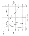
- Figure 9 depicts the frequency response of a 8.34dB edge-coupled microstrip coupler configured as a balun
- Figure 10 is illustrative of the frequency response of two 8.34dB couplers configured in a tandem configuration as shown in Figures 1-4.
- reference numeral 62 denotes the return loss
- reference numeral 64 denotes the insertion loss of each of the two couplers C 1 and C 2 .
- the return loss 62 peaks at around 1000MHz.
- the minimum insertion loss occurs at the same frequency, but falls off sharply on either side of about -0.2dB.
- the composite return loss as indicated by reference numeral 66 in Figure 10 dips to about -40dB at around 1500MHz.
- the composite insertion loss, as indicated by curve 68 of Figure 10 is indicative of a change of only about 0.25dB over a bandwidth of almost 1000MHz, thus illustrating the broadband result achieved by the subject invention.
Landscapes
- Coils Or Transformers For Communication (AREA)
- Near-Field Transmission Systems (AREA)
- Cable Transmission Systems, Equalization Of Radio And Reduction Of Echo (AREA)
- Transmitters (AREA)
- Waveguides (AREA)
Claims (26)
- Übertragungsleitungs-Symmetrieübertrager zum Bilden eines unsymmetrischen Ausgangssignals aus einem Paar von Differenzeingangssignalen, aufweisend:einen ersten Übertragungsleitungssignalkoppler (C1) und einen zweiten Übertragungsleitungssignalkoppler (C2) mit einer entsprechenden Kopplungscharakteristik, wobei die Koppler elektromagnetisch voneinander isoliert sind und Übertragungsleitungselemente (a1, a2, b1, b2) aufweisen,dadurch gekennzeichnet,
dass die Koppler überkreuz hintereinandergekoppelt sind (10, 11) und zwischen sich eine Rückkopplungsverbindung (9) aufweisen, um so eine vorbestimmte Signalphasenlage zu liefern, wodurch eine verbesserte Gesamtkopptungscharakteristik bezüglich der entsprechenden Kopplungscharakteristik des ersten und des zweiten Signalkopplers erzielt wird. - Symmetrieübertrager nach Anspruch 1, wobei die Kopplungscharakteristik beider Koppler im Wesentlichen dieselbe ist.
- Symmetrieübertrager nach Anspruch 1, wobei die Kopplungscharakteristiken beider Koppler beiderseits unterschiedlich sind.
- Symmetrieübertrager nach Anspruch 1, wobei die Kopplungscharakteristik von mindestens einem der Koppler mehr als 3dB beträgt.
- Symmetrieübertrager nach Anspruch 1, wobei die Kopplungscharakteristik von mindestens einem Koppler aus [der Gesamtheit aus] dem ersten Koppler und dem zweiten Koppler größer als 3dB ist, und wobei die Gesamtkopplungscharakteristik ungefähr gleich oder größer als 3dB ist.
- Symmetrieübertrager nach Anspruch 1, wobei das erste Paar von Übertragungsleitungselementen und das zweite Paar von Übertragungsleitungselementen für eine beabsichtigte Anwendung spezifische vorbestimmte körperliche Abmessungen sowie Beabstandungen aufweisen.
- Symmetrieübertrager nach Anspruch 1, wobei jeder der Koppler jeweils Paare von Übertragungsleitungselementen mit entsprechenden Eingangsenden (1, 3, 5, 7) und Ausgangsenden (2, 4, 6, 8) aufweist und wobei die Ausgangsenden des ersten Signalkopplers überkreuz mit den Eingangsenden des zweiten Signalkopplers gekoppelt sind und ein Ausgangsende des zweiten Signalkopplers mit dem einen Eingangsende des ersten Signalkopplers rückverbunden ist.
- Symmetrieübertrager nach Anspruch 6, wobei die Paare von Übertragungsleitungselementen eigenständige Längen von Leitermaterial beinhalten.
- Symmetrieübertrager nach Anspruch 8, wobei die Längen des Leitermaterials gegenseitig parallel zueinander angeordnet sind.
- Symmetrieübertrsger nach Anspruch 8, wobei die Längen des Halbleitermaterials gegenseitig gewinkelt sind, um so dazwischen eine sich verjüngende Beabstandung zu liefern.
- Symmetrieübertrager nach Anspruch 7, wobei die Paare von Übertragungsleitungselementen eigenständige Längen von Leitermaterial beinhalten, die von einem Ende zum anderen eine verjüngte Breitendimension aufweisen.
- Symmetrieübertrager nach Anspruch 7, wobei die Paare von Übertragungsleitungselementen eigenständige Längen von Leitermaterial beinhalten, die sich gegenseitig gegenüberstehende, gezackte Kanten aufweisen.
- Symmetrieübertrager nach Anspruch 1, wobei die Paare von Übertragungsleitungselementen Übertragungsleitungselemente mit einer Länge von ungefähr einem Viertel der Wellenlänge aufweisen.
- Symmetrieübertrager nach Anspruch 1, wobei die Paare von Übertragungsleitungselementen jeweils auf gegenüberliegenden Seitenbereichen (22, 24) eines dielektrischen Halterungselementes angeordnet sind.
- Symmetrieübertrager nach Anspruch 14, wobei das dielektrische Halterungselement ein Platinenelement einschließlich einer Zwischenschicht elektrisch leitfähigen Materials (30) zum Isolieren der Paare von Übertragungsleitungselementen aufweist.
- Symmetrieübertrager nach Anspruch 15, wobei die Zwischenschicht aus elektrisch leitfähigem Material mindestens einer Öffnung (32, 34) darin beinhaltet, um so elektrische Verbindungen zwischen den Paaren von Übertragungsleitungselementen zu erleichtern.
- Symmetrieübertrager nach Anspruch 16, der ferner Durchgangslöcher (9, 10, 11, 12) in dem Platinenelement aufweist, und die zum Überkreuzverbinden der Enden der Übertragungsleitungselemente und zum Verbinden des einen Ausgangsendes des zweiten Signalkopplers mit dem einen Eingangsende des ersten Signalkopplers durch die mindestens eine Öffnung in der Zwischenschicht aus leitfähigem Material hindurchtreten.
- Symmetrieübertrager nach Anspruch 15, ferner aufweisend ein Paar von Eingangsanschlüssen (P1, P2) und einen einzigen Ausgangsanschluss (P3), die gemeinsam entlang einer gemeinsamen Kante (36) des Platinenelementes zum Koppeln von Signalen zu und von dem Symmetrieübertrager angeordnet sind.
- Symmetrieübertrager nach Anspruch 15, wobei mindestens eines der Paare von Übertragungsleitungselementen auf einer äußeren Oberfläche des Platinenelementes angeordnet ist.
- Symmetrieübertrager nach Anspruch 14, wobei die Paare von Übertragungsleitungselementen Paare von parallelen Übertragungsleitungselementen aufweisen, die entsprechend auf einer äußeren Oberfläche (26, 28) der sich gegenüberstehenden Seitenbereiche des Platinenelementes angeordnet sind.
- Symmetrieübertrager nach Anspruch 14, wobei beide Paare von Übertragungsleitungselementen auf entsprechenden äußeren Oberflächen des Platinenelementes angeordnet sind.
- Symmetrieübertrager nach Anspruch 19, wobei die Übertragungsleitungselemente Mikrostreifenleiter umfassen.
- Symmetrieübertrager nach Anspruch 14, zusätzlich aufweisend ein Paar dielektrischer Elemente (54, 56), die entsprechend an gegenüberliegenden Seiten der dielektrischen Halterung angeordnet sind, welche den gegenüberstehenden Seitenbereichen und den entsprechenden Schichten elektrisch leitfähigen Materials (58, 60) auf einer oberen Oberfläche des Paares dielektrischer Elemente gemeinsam sind.
- Symmetrieübertrager nach Anspruch 21, wobei die Paare von Übertragungsleitungselementen Streifenleiter beinhalten.
- Symmetrieübertrager nach Anspruch 15,
wobei die Übertragungsleitungselemente Viertelwellenlängen-Mikrostreifenübertragungsleitungselemente beinhalten;
wobei jedes Paar von Übertragungsleitungselementen entsprechende erste und zweite Eingangsenden und erste und zweite Ausgangsenden aufweist, und
wobei auf einer Kante des Platinenelementes das erste Eingangsende und das zweite Eingangsende mit einem Paar von Eingangsanschlüssen verbunden sind, wobei das erste Ausgangsende und das zweite Ausgangsende des ersten Signalkopplers überkreuz mit dem zweiten Eingangsende und dem ersten Eingangsende des zweiten Signalkopplers verbunden ist, wobei das erste Ausgangsende des zweiten Signalkopplers mit einem auf der Kante des Platinenelementes angeordneten Ausgangsanschluss verbunden ist, und das zweite Ausgangsende des zweiten Signalkopplers mit dem ersten Eingangsende des ersten Signalkopplers verbunden ist. - Symmetrieübertrager nach Anspruch 15,
wobei die Übertragungsleitungselemente Viertelwellenlängen-Streifenleiterübertragungselemente beinhalten,
wobei entsprechende dielektrische Elemente eine äußere Metallisierungsschicht aufweisen, die über den Paaren von Übertragungsleitungselementen angeordnet ist;
wobei jedes Paar von Übertragungsleitungselementen entsprechend ein erstes Eingangsende und ein zweites Eingangsende und ein erstes Ausgangsende und ein zweites Ausgangsende aufweist; und wobei das erste Eingangsende und das zweite Eingangsende mit einem Paar von Eingangsanschlüssen auf einer Kante des Platinenelementes verbunden sind, wobei das erste Ausgangsende und das zweite Ausgangsende des ersten Signalkopplers überkreuz mit dem zweiten Eingangsanschluss und dem ersten Eingangsanschluss des zweiten Signalkopplers verbunden ist, wobei das erste Ausgangsende des zweiten Signalkopplers mit einem auf der Kante des Platinenelementes angeordneten Ausgangsanschlusses verbunden ist, und das zweite Ausgangsende des zweiten Signalkopplers mit dem ersten Eingangsende des ersten Signalkopplers verbunden ist.
Applications Claiming Priority (2)
| Application Number | Priority Date | Filing Date | Title |
|---|---|---|---|
| US257014 | 1999-02-25 | ||
| US09/257,014 US6140886A (en) | 1999-02-25 | 1999-02-25 | Wideband balun for wireless and RF application |
Publications (2)
| Publication Number | Publication Date |
|---|---|
| EP1032071A1 EP1032071A1 (de) | 2000-08-30 |
| EP1032071B1 true EP1032071B1 (de) | 2007-12-26 |
Family
ID=22974539
Family Applications (1)
| Application Number | Title | Priority Date | Filing Date |
|---|---|---|---|
| EP00301171A Expired - Lifetime EP1032071B1 (de) | 1999-02-25 | 2000-02-15 | Breitbandige Symmetrierschaltung für drahtlose und hochfrequente Anwendungen |
Country Status (6)
| Country | Link |
|---|---|
| US (1) | US6140886A (de) |
| EP (1) | EP1032071B1 (de) |
| JP (1) | JP3691710B2 (de) |
| CN (1) | CN1271976A (de) |
| CA (1) | CA2298223C (de) |
| DE (1) | DE60037550T2 (de) |
Families Citing this family (19)
| Publication number | Priority date | Publication date | Assignee | Title |
|---|---|---|---|---|
| JP3119250B2 (ja) * | 1998-10-26 | 2000-12-18 | 日本電気株式会社 | 180度移相器 |
| US6538614B2 (en) | 2001-04-17 | 2003-03-25 | Lucent Technologies Inc. | Broadband antenna structure |
| JP2003008311A (ja) * | 2001-06-22 | 2003-01-10 | Mitsubishi Electric Corp | バランおよび該バランを有する半導体装置 |
| SE522404C2 (sv) * | 2001-11-30 | 2004-02-10 | Ericsson Telefon Ab L M | Riktkopplare |
| US7138884B2 (en) * | 2002-08-19 | 2006-11-21 | Dsp Group Inc. | Circuit package integrating passive radio frequency structure |
| KR100526239B1 (ko) * | 2002-09-27 | 2005-11-08 | 삼성전기주식회사 | 3 라인 발룬 트랜스포머 |
| US7605672B2 (en) * | 2006-02-02 | 2009-10-20 | Anaren, Inc. | Inverted style balun with DC isolated differential ports |
| US20080018344A1 (en) * | 2006-07-21 | 2008-01-24 | Jachim Stephen P | RF Bridge Circuit Without Balun Transformer |
| US7728694B2 (en) * | 2007-07-27 | 2010-06-01 | Anaren, Inc. | Surface mount stripline devices having ceramic and soft board hybrid materials |
| US8232851B2 (en) * | 2009-03-16 | 2012-07-31 | International Business Machines Corporation | On-chip millimeter wave lange coupler |
| JP2011045008A (ja) * | 2009-08-24 | 2011-03-03 | Sony Corp | 結合器及び通信システム |
| US8611436B2 (en) * | 2011-07-19 | 2013-12-17 | Tektronix, Inc. | Wideband balun structure |
| US9130252B2 (en) * | 2013-02-26 | 2015-09-08 | Raytheon Company | Symmetric baluns and isolation techniques |
| US9625508B2 (en) * | 2014-01-27 | 2017-04-18 | Vayyar Imaging Ltd. | Vector network analyzer |
| CN104993206A (zh) * | 2015-07-29 | 2015-10-21 | 胡雨思 | 小型化定向耦合器 |
| CN104979611A (zh) * | 2015-07-29 | 2015-10-14 | 胡雨思 | 可调节定向耦合器 |
| CN109088137B (zh) * | 2018-08-31 | 2022-03-01 | 易力声科技(深圳)有限公司 | 一种应用于双面平行线的集总电路平衡转换器 |
| JP7434948B2 (ja) * | 2020-01-31 | 2024-02-21 | Tdk株式会社 | 積層型バラン |
| CN117497989B (zh) * | 2024-01-03 | 2024-03-08 | 南京迈矽科微电子科技有限公司 | 功率分配器及一种电子设备 |
Citations (1)
| Publication number | Priority date | Publication date | Assignee | Title |
|---|---|---|---|---|
| GB2311417A (en) * | 1996-03-22 | 1997-09-24 | Murata Manufacturing Co | Laminated balun transformer |
Family Cites Families (3)
| Publication number | Priority date | Publication date | Assignee | Title |
|---|---|---|---|---|
| US3991390A (en) * | 1975-07-31 | 1976-11-09 | Motorola, Inc. | Series connected stripline balun |
| US5774801A (en) * | 1995-08-23 | 1998-06-30 | Ericsson Inc. | High dynamic range mixer having low conversion loss, low local oscillator input power, and high dynamic range and a method for designing the same |
| FI103614B1 (fi) * | 1997-03-20 | 1999-07-30 | Nokia Mobile Phones Ltd | Vaiheistus- ja balansointielin |
-
1999
- 1999-02-25 US US09/257,014 patent/US6140886A/en not_active Expired - Lifetime
-
2000
- 2000-02-09 CA CA002298223A patent/CA2298223C/en not_active Expired - Fee Related
- 2000-02-15 DE DE60037550T patent/DE60037550T2/de not_active Expired - Lifetime
- 2000-02-15 EP EP00301171A patent/EP1032071B1/de not_active Expired - Lifetime
- 2000-02-24 CN CN00102607A patent/CN1271976A/zh active Pending
- 2000-02-25 JP JP2000048693A patent/JP3691710B2/ja not_active Expired - Fee Related
Patent Citations (1)
| Publication number | Priority date | Publication date | Assignee | Title |
|---|---|---|---|---|
| GB2311417A (en) * | 1996-03-22 | 1997-09-24 | Murata Manufacturing Co | Laminated balun transformer |
Also Published As
| Publication number | Publication date |
|---|---|
| CA2298223C (en) | 2002-10-15 |
| EP1032071A1 (de) | 2000-08-30 |
| DE60037550D1 (de) | 2008-02-07 |
| JP3691710B2 (ja) | 2005-09-07 |
| CN1271976A (zh) | 2000-11-01 |
| CA2298223A1 (en) | 2000-08-25 |
| US6140886A (en) | 2000-10-31 |
| DE60037550T2 (de) | 2009-01-08 |
| JP2000252710A (ja) | 2000-09-14 |
Similar Documents
| Publication | Publication Date | Title |
|---|---|---|
| EP1032071B1 (de) | Breitbandige Symmetrierschaltung für drahtlose und hochfrequente Anwendungen | |
| EP0885469B1 (de) | Hochfrequenz-symmetriereinrichtung in einem mehrschichtsubstrat | |
| US7138887B2 (en) | Coupler with lateral extension | |
| US7009467B2 (en) | Directional coupler | |
| US6133806A (en) | Miniaturized balun transformer | |
| US7190240B2 (en) | Multi-section coupler assembly | |
| US7605672B2 (en) | Inverted style balun with DC isolated differential ports | |
| US4737740A (en) | Discontinuous-taper directional coupler | |
| US4532484A (en) | Hybrid coupler having interlaced coupling conductors | |
| US5432487A (en) | MMIC differential phase shifter | |
| US4288761A (en) | Microstrip coupler for microwave signals | |
| EP0417590B1 (de) | Flaches magisches Tee in Luftstreifenleitungs-/Streifenleitungstechnik | |
| US6891448B2 (en) | Compact balun for 802.11a applications | |
| US4636754A (en) | High performance interdigitated coupler with additional jumper wire | |
| US9325051B1 (en) | Resonance-inhibiting transmission-line networks and junction | |
| KR20180047697A (ko) | 이중대역 합성 우좌향 전송선로 및 이를 이용한 이중 대역 브랜치 라인 하이브리드 커플러 | |
| EP1042843B1 (de) | Rf-dreiwegkombinierer/-verteiler | |
| WO2018128968A1 (en) | Transmission line transformers | |
| US9966646B1 (en) | Coupler with lumped components | |
| US5959509A (en) | Printed 180 degree differential phase shifter including a non-uniform non-regular line | |
| KR100317226B1 (ko) | 아이솔레이터 | |
| EP1987562A2 (de) | Symmetrierer des umgekehrten stils mit gleichstromisolierten differenzports |
Legal Events
| Date | Code | Title | Description |
|---|---|---|---|
| PUAI | Public reference made under article 153(3) epc to a published international application that has entered the european phase |
Free format text: ORIGINAL CODE: 0009012 |
|
| AK | Designated contracting states |
Kind code of ref document: A1 Designated state(s): AT BE CH CY DE DK ES FI FR GB GR IE IT LI LU MC NL PT SE |
|
| AX | Request for extension of the european patent |
Free format text: AL;LT;LV;MK;RO;SI |
|
| 17P | Request for examination filed |
Effective date: 20010222 |
|
| AKX | Designation fees paid |
Free format text: AT BE CH CY DE DK ES FI FR GB GR IE IT LI LU MC NL PT SE |
|
| 17Q | First examination report despatched |
Effective date: 20061121 |
|
| GRAP | Despatch of communication of intention to grant a patent |
Free format text: ORIGINAL CODE: EPIDOSNIGR1 |
|
| RBV | Designated contracting states (corrected) |
Designated state(s): DE FI FR SE |
|
| GRAS | Grant fee paid |
Free format text: ORIGINAL CODE: EPIDOSNIGR3 |
|
| GRAA | (expected) grant |
Free format text: ORIGINAL CODE: 0009210 |
|
| AK | Designated contracting states |
Kind code of ref document: B1 Designated state(s): DE FI FR SE |
|
| REF | Corresponds to: |
Ref document number: 60037550 Country of ref document: DE Date of ref document: 20080207 Kind code of ref document: P |
|
| PG25 | Lapsed in a contracting state [announced via postgrant information from national office to epo] |
Ref country code: SE Free format text: LAPSE BECAUSE OF FAILURE TO SUBMIT A TRANSLATION OF THE DESCRIPTION OR TO PAY THE FEE WITHIN THE PRESCRIBED TIME-LIMIT Effective date: 20080326 |
|
| PG25 | Lapsed in a contracting state [announced via postgrant information from national office to epo] |
Ref country code: FI Free format text: LAPSE BECAUSE OF FAILURE TO SUBMIT A TRANSLATION OF THE DESCRIPTION OR TO PAY THE FEE WITHIN THE PRESCRIBED TIME-LIMIT Effective date: 20071226 |
|
| ET | Fr: translation filed | ||
| PLBE | No opposition filed within time limit |
Free format text: ORIGINAL CODE: 0009261 |
|
| STAA | Information on the status of an ep patent application or granted ep patent |
Free format text: STATUS: NO OPPOSITION FILED WITHIN TIME LIMIT |
|
| 26N | No opposition filed |
Effective date: 20080929 |
|
| PGFP | Annual fee paid to national office [announced via postgrant information from national office to epo] |
Ref country code: FR Payment date: 20140211 Year of fee payment: 15 |
|
| PGFP | Annual fee paid to national office [announced via postgrant information from national office to epo] |
Ref country code: DE Payment date: 20140417 Year of fee payment: 15 |
|
| REG | Reference to a national code |
Ref country code: DE Ref legal event code: R082 Ref document number: 60037550 Country of ref document: DE Representative=s name: DILG HAEUSLER SCHINDELMANN PATENTANWALTSGESELL, DE |
|
| REG | Reference to a national code |
Ref country code: DE Ref legal event code: R119 Ref document number: 60037550 Country of ref document: DE |
|
| REG | Reference to a national code |
Ref country code: FR Ref legal event code: ST Effective date: 20151030 |
|
| PG25 | Lapsed in a contracting state [announced via postgrant information from national office to epo] |
Ref country code: DE Free format text: LAPSE BECAUSE OF NON-PAYMENT OF DUE FEES Effective date: 20150901 |
|
| PG25 | Lapsed in a contracting state [announced via postgrant information from national office to epo] |
Ref country code: FR Free format text: LAPSE BECAUSE OF NON-PAYMENT OF DUE FEES Effective date: 20150302 |