EP1032075A2 - Elektrischer Verbinder für Schleifenantennen - Google Patents
Elektrischer Verbinder für Schleifenantennen Download PDFInfo
- Publication number
- EP1032075A2 EP1032075A2 EP00103313A EP00103313A EP1032075A2 EP 1032075 A2 EP1032075 A2 EP 1032075A2 EP 00103313 A EP00103313 A EP 00103313A EP 00103313 A EP00103313 A EP 00103313A EP 1032075 A2 EP1032075 A2 EP 1032075A2
- Authority
- EP
- European Patent Office
- Prior art keywords
- connector
- block
- terminal
- face
- generally
- Prior art date
- Legal status (The legal status is an assumption and is not a legal conclusion. Google has not performed a legal analysis and makes no representation as to the accuracy of the status listed.)
- Withdrawn
Links
Images

Classifications
-
- H—ELECTRICITY
- H01—ELECTRIC ELEMENTS
- H01Q—ANTENNAS, i.e. RADIO AERIALS
- H01Q7/00—Loop antennas with a substantially uniform current distribution around the loop and having a directional radiation pattern in a plane perpendicular to the plane of the loop
-
- H—ELECTRICITY
- H01—ELECTRIC ELEMENTS
- H01R—ELECTRICALLY-CONDUCTIVE CONNECTIONS; STRUCTURAL ASSOCIATIONS OF A PLURALITY OF MUTUALLY-INSULATED ELECTRICAL CONNECTING ELEMENTS; COUPLING DEVICES; CURRENT COLLECTORS
- H01R13/00—Details of coupling devices of the kinds covered by groups H01R12/70 or H01R24/00 - H01R33/00
- H01R13/02—Contact members
- H01R13/10—Sockets for co-operation with pins or blades
- H01R13/11—Resilient sockets
- H01R13/113—Resilient sockets co-operating with pins or blades having a rectangular transverse section
-
- H—ELECTRICITY
- H01—ELECTRIC ELEMENTS
- H01R—ELECTRICALLY-CONDUCTIVE CONNECTIONS; STRUCTURAL ASSOCIATIONS OF A PLURALITY OF MUTUALLY-INSULATED ELECTRICAL CONNECTING ELEMENTS; COUPLING DEVICES; CURRENT COLLECTORS
- H01R2201/00—Connectors or connections adapted for particular applications
- H01R2201/02—Connectors or connections adapted for particular applications for antennas
-
- Y—GENERAL TAGGING OF NEW TECHNOLOGICAL DEVELOPMENTS; GENERAL TAGGING OF CROSS-SECTIONAL TECHNOLOGIES SPANNING OVER SEVERAL SECTIONS OF THE IPC; TECHNICAL SUBJECTS COVERED BY FORMER USPC CROSS-REFERENCE ART COLLECTIONS [XRACs] AND DIGESTS
- Y10—TECHNICAL SUBJECTS COVERED BY FORMER USPC
- Y10S—TECHNICAL SUBJECTS COVERED BY FORMER USPC CROSS-REFERENCE ART COLLECTIONS [XRACs] AND DIGESTS
- Y10S439/00—Electrical connectors
- Y10S439/94—Electrical connectors including provision for mechanical lifting or manipulation, e.g. for vacuum lifting
Definitions
- the present invention relates to an electrical connector for being mounted on a board and for connecting a loop antenna or the like to a circuit on the board.
- the present invention is for such an electrical connector comprising a connector block and first and second terminals mounted to the connector block.
- a relatively small loop antenna is connected to a circuit on a board within such pager.
- such loop antenna receives pager signals broadcast from a remote source, and couples such received signals to the circuit on the board within the pager.
- Such loop antenna may also transmit signals from the circuit on the board to the remote source.
- the present invention satisfies the aforementioned needs by providing an electrical connector for being mounted on a board and for connecting a loop antenna or the like to a circuit on the board.
- the connector has a connector block and first and second terminals.
- the connector block is constructed from a non-conductive material and has generally opposing top and bottom faces, first and second generally opposing side faces, and a center portion extending between the top face and bottom face.
- the center portion defines first and second bays isolated from each other, where the first and second bays are exposed at the top and bottom faces. The first bay is further exposed at the first side face, and the second bay is further exposed at the second side face.
- the first and second terminals are mounted in the first and second bays of the connector block.
- Each terminal is constructed from a conductive material and has an open jaw generally positioned at the top face of the connector block, and a contacting portion generally opposite the open jaw and generally positioned at the bottom face of the connector block.
- the antenna connector is mounted to the board such that the bottom face of the connector block faces the board, and such that the contacting portions of the first and second terminals are in electrical contact with corresponding pads on such board.
- the first terminal receives a first end of the loop antenna
- the second terminal receives a second end of the loop antenna
- Fig. 1 an electrical connector 10a in accordance with one embodiment of the present invention.
- the connector 10a is for being mounted on a printed circuit board 12 or the like, and is for connecting a loop antenna 14 or the like to a circuit on the board 12.
- the printed circuit board 12 may fit within a personal pager that requires a receiving and perhaps transmitting loop antenna 14. Since the typical personal pager is relatively small, the printed circuit board 12 is also relatively small as is the loop antenna 14.
- the loop antenna 14 may have a defined perimeter of about two inches by about one half inch.
- loop antenna 14 loops from a first end off and under the printed circuit board 12 and then back up and on to the printed circuit board 12 at a second end.
- loop antenna 14 loops from a first end off and under the printed circuit board 12 and then back up and on to the printed circuit board 12 at a second end.
- other antenna configurations may be employed without departing from the spirit and scope of the present invention.
- the connector 10a includes a connector block 16 flanked by first and second terminals 18. Note that the same connector 10a is shown in Fig. 1, although the connector block 16 is shown in phantom in Fig. 1 for purposes of clarity in viewing the first and second terminals 18 shown therein.
- the connector block 16 is preferably constructed from a non-conductive insulative material such as a polymer, a ceramic, an elastomeric material, or the like. However, other non-conductive materials may be employed without departing from the spirit and scope of the present invention.
- the connector block 16 has generally opposing top and bottom faces 20t, 20b, first and second generally opposing side faces 22a, 22b, and generally opposing back and front faces 24b, 24f.
- each face 20t, 20b, 22a, 22b, 24b, 24f corresponds to a presentation of a side of the connector block 16 and not necessarily to a particular physical aspect of such side.
- the connector block 16 has a center portion 26 that extends between the top face 20t and the bottom face 20b and that defines first and second bays 28a, 28b that are isolated from each other by such center portion 26. As also seen, the center portion 26 extends between the front face 24f and the back face 24b.
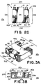
- first and second bays, 28a, 28b are exposed at the top and bottom faces 20t, 20b of the connector block 16. Moreover, the first bay 28a is exposed at the first side face 22a, and the second bay 28b is exposed at the second side face 22b. In fact in the embodiment shown in Figs. 2A-2C, such bays 28a, 28b are relatively largely exposed and relatively minimally defined by the connector block 16. However, and as will be seen below, in other embodiments of the present invention, such first and second bays 28a, 28b may be relatively minimally exposed and relatively largely defined by the connector block 16 while still being within the spirit and scope of the present invention.
- the first and second terminals 18 are mounted in the first and second bays 28a, 28b of the connector block 16. As seen, the first and second terminals 18 are generally identical, although it will be recognized that non-identical first and second terminals 18 may be employed without departing from the spirit and scope of the present invention.
- Each of the first and second terminals 18 is constructed from a conductive material, such as a brass material, a bronze material, a stainless steel material, a copper material, or the like.
- each terminal 18 has an open jaw 30 generally positioned at the top face 20t of the connector block 16.
- each terminal 18 has a contacting portion 32 generally opposite the open jaw 30 and generally positioned at the bottom face 20B of the connector block 16.
- the connector 10a is mounted to the board 12 such that the bottom face 20b of the connector block 16 faces the board 12 and such that the contacting portions 32 of the first and second terminals 18 are in electrical contact with corresponding pads (not shown) on such board 12.
- contacting portions 32 are soldered in place in the aforementioned electrical contact with the corresponding pads to secure the first and second terminals 18 to the board 12.
- soldering may be achieved by any known soldering process.
- other methods of securely electrically connecting the contacting portions 32 to the pads to secure the terminal 18 to the board may be employed without departing from the spirit and scope of the present invention. As but one example, brazing may be employed.
- the connector block 16 may also be secured to the board 12 by any appropriate means. As should be understood, and still referring to Fig. 1, the first terminal 18 receives the first end of the loop antenna 14 and the second terminal 18 receives the second end of the loop antenna 14.
- the top face 20t of the connector block 16 includes a generally flat top surface 34. More preferably, the flat top surface 34 is associated with the center portion 26 such that such center portion 26 extends between the flat top surface 34 of the top face 20t and the bottom face 20b.
- a vacuum pick-and-place machine (not shown) in an automated fashion and placed in mounting relation to the board 12. Accordingly, such placing operation may be automated.
- Such vacuum pick-and-place machines and their operation are known and therefore need not be further described herein any detail.
- non-vacuum pick-and-place machines may be employed to pick up and place the connector 10a in an automated manner without departing from the spirit and scope of the present invention.
- a grabber-type pick-and-place machine may be employed, and may user grabbers that grab at the front and back faces 24f, 24b of the connector 10a in the region of the center portion 26.
- Such grabber-type and other non-vacuum pick-and-place machines and their operation are known and therefore need not be further described herein any detail. If in fact such a non-vacuum machine is employed, the aforementioned top surface 34 need not necessarily be flat
- the bottom face 20b may also comprise a generally flat bottom surface 36 (Fig. 2B) such tat the connector 10a when placed in mounting relation to the board 12 is in intimate contact therewith.
- a generally flat bottom surface 36 Fig. 2B
- Such flat bottom surface 36 is not believed necessary to the present invention, and circumstances may in fact dictate that the bottom surface 36 have a predefined contour.
- such bottom surface 36 may have a series of alignment posts (not shown) keyed to a series of apertures (not shown) in the board 12 such that the posts and apertures precisely position the connector block 16 and connector 10a on the board 12.
- each contacting portion 32 of each terminal 18 be generally flat, that each contacting portion 32 reside in a plane generally parallel to the bottom surface 36 / bottom face 20b of the connector block 16.
- each contacting portion 32 is indeed generally coextensive with the bottom surface 20b / bottom face 36 of the connector block 16.
- each terminal 18 is preferably a snap-in terminal 18 such that the first end of the loop antenna 14 snaps into the first terminal 18 and the second end of the loop antenna 14 snaps into the second terminal 18. More preferably, each terminal 18 is generally U-shaped and has a pair of side portions 38 that extend from the contacting portion 32 and define the open jaw 30. Alternatively, each terminal 18 has only one side portion 38 which cooperates with an opposing body that is not part of the terminal 18 to define the open jaw 30 (not shown). In the preferred case of a pair of side portions, and as best seen in Figs.
- each side portion 38 generally exhibits an S-shape such that the part of the side portion 38 adjacent the top surface 34 of the connector block 16 flares out
- each side portion 38 is reasonably compliant and the bays 28a, 28b are sized to reasonably allow compliant movement of such side portions. Accordingly, and as should be evident, such flaring, such compliance, and such sizing all contribute to facilitate the snap-in function.
- the first and second ends of the loop antenna preferably maintain an interference fit within the respective first and second terminals 18. Accordingly, each end maintains good electrical contact with the respective terminal and cannot move around within such respective terminal.
- the connector block 16 has a front portion 40f that extends along the front face 24f between the first and second side faces. As should be appreciated, such front portion 40f further defines the first and second bays. As seen in Figs. 2A-2C, the front portion 40f includes a front part of the center portion 26, and has half-high wings that extend from such center portion 26 toward the first and second side faces 22a, 22b of the connector block 16.
- the front portion 40f may have another design without departing from the spirit and scope of the invention, as long as such other design is consistent with the function of such front portion 40f, as will be described below.
- the front portion 40f has an aperture 42 extending thereinto from each bay 28a, 28b, and each terminal 18 has an extending member 44 that extends into the aperture 42 to anchor such terminal 18 to the connector block 16.
- each aperture 42 and each extending member 44 extends through the front portion 40f in a direction generally perpendicular to the front face 24f of the connector block 16.
- the aperture 42 and extending member 44 may extend into the front portion 40f a shortened distance and at a slight upward inclination.
- the extending member 44 is keyed to the aperture 42 to the extent necessary to prevent rotation or other similar movement of the extending member 44 within the aperture 42.
- the extending member 44 may maintain an interference fit with the aperture 42.
- the extending member 44 may be secured in the aperture 42 by glue, epoxy, or other securing materials. If not secured as such, the connector block 16 could be removed (by machine or otherwise) after the terminals 18 have been soldered in place on the board 12. Note, though, that it may be preferable to leave the connector block 16 in place, such as to define and/or limit the placement of the loop antenna 14.
- the extending member 44 is separated from the adjacent side portion 38 of the terminal 18, and ten folded down and out.
- such adjacent side portion 38 is provided with a pair of slits to define a middle sub-portion between two exterior sub-portions, and the middle portion is bent down to form the extending member 44 while leaving the remaining exterior portions as such side portion 38.
- any appropriate method of formation may be employed to form the extending portion 44 without departing from the spirit and scope of the present invention.
- molding or bending may be employed in any of a variety of ways.
- an electrical connector 10b is shown in accordance with another embodiment of the present invention.
- the connector 10b is similar to the connector 10a except that the connector block 16 of the connector 10b has, in addition to a front portion 40f, a back portion 40b that extends along the back face 24b between the first and second side faces 22a, 22b.
- back portion 40b further defines the first and second bays 28a, 28b in combination with the front portion 40f.
- the front portion 40f and back portion 40b both include a part of the center portion 26, and have full-height wings that extend from such center portion 26 toward the first and second side faces 22a, 22b of the connector block 16.
- the front portion 40f and back portion 40b of the embodiment shown in Figs. 3A and 3B may have another design without departing from the spirit and scope of the invention, as long as such other design is consistent with the function of such front portion 40f and back portion 40b, as will be described below.
- each terminal 18 has the same general U-shape as before. However, no extending portion is provided. Rather, the side portions 38 of each terminal 18 extend generally along the front portion 40f and the back portion 40b, respectively, of the connector block 16. As should now be understood, such side portions 38 are arranged at an appropriate pitch with respect to the contacting portion 32 to allow such side portions 38 and such terminal 18 to maintain an interference fit in the respective bay 28a, 28b between the front portion 40f and the back portion 40b.
- each bay 28a, 28b includes front and back projections 46 that extend into the bay from the front portion 40f and back portion 40b, respectively. More preferably, the projections 46 extend toward the side portions 38 and cooperate with the bent area of the side portion 38 adjacent the flared out area thereof Accordingly, such projections 46 support each terminal, assist in maintaining the interference fit of each terminal, and prevent the terminal from moving in a direction perpendicular to the top face 20t of the connector block 16. Of course, such projections 46 should not impede the snap-in function of the terminals 18.
- the connector 10a could be symmetrical as between the first and second side faces 22a, 22b.
- the connector 10b could also be symmetrical as between the first and second side faces 22a, 22b; and in addition be symmetrical as between the front and back faces 24a, 24b.
- Such double symmetry could be useful in that either face 24a, 24b may be 'the front face 24a'.
- such double symmetry in the connector 10b, and the single symmetry in the connector 10a are not required for practicing the present invention.
- the first and second terminals 18 are ranged in the first and second bays 28a, 28b of the connector block 16 such that the loop antenna 14 extends away from the first side face 22a of the connector block 16 adjacent the first end of such loop antenna 14, and such that the loop antenna 14 extends away from the second side face 22b of the connector block 16 adjacent the second end of such loop antenna 14.
- the first end of the loop antenna 14 approaches toward the first side face 22a of the connector block 16 and the second end of the loop antenna 14 approaches toward the second side face 22b of the connector block 16.
- the first end may instead approach toward the front face 24a of the connector block 16 and the second end may instead approach toward the back face 24b of the connector block 16.
- the connector 10a, 10b is also relatively small.
- the center portion 26 of the connector block 16 has a width of about 0.08 inches and a depth of about 0.17 inches
- each terminal 18 has a width of about 0.06 inches and a depth of about 0.12 inches
- the center-lines of the terminals 18 are spaced apart about 0.14 inches.
- other dimensions may be employed without departing from the spirit and scope of the present invention.
- the present invention comprises a new and useful connector 10a, 10b for being mounted on a board 12 and for connecting a loop antenna 14 to a circuit on the board 12.
- such connector 10a, 10b can be machine mounted on a board via an appropriate pick-and place machine or the like, and the loop antenna 14 can likewise be machine connected to such connector 10a, 10b via appropriate machinery (not shown).
- multiple terminals 18 may be employed in the connector 10a, 10b for receiving each end of the loop antenna 14 (not shown).
- multiple extending members 44 may be peeled off from the adjacent side portion 38 of the terminal 18 of the connector 10a, thereby leaving a number interior sub-portions as well as two exterior sub-portions (not shown). In either case, retention of each end of the loop antenna 14 is improved, as is the electrical connection. It should be understood, therefore, that this invention is not limited to the particular embodiments disclosed, but it is intended to cover modifications within the spirit and scope of the present invention as defined by the appended claims.
Landscapes
- Coupling Device And Connection With Printed Circuit (AREA)
- Support Of Aerials (AREA)
- Connections Arranged To Contact A Plurality Of Conductors (AREA)
Applications Claiming Priority (2)
| Application Number | Priority Date | Filing Date | Title |
|---|---|---|---|
| US09/259,006 US6149470A (en) | 1999-02-26 | 1999-02-26 | Electrical connector for antenna or the like |
| US259006 | 1999-02-26 |
Publications (2)
| Publication Number | Publication Date |
|---|---|
| EP1032075A2 true EP1032075A2 (de) | 2000-08-30 |
| EP1032075A3 EP1032075A3 (de) | 2003-01-08 |
Family
ID=22983099
Family Applications (1)
| Application Number | Title | Priority Date | Filing Date |
|---|---|---|---|
| EP00103313A Withdrawn EP1032075A3 (de) | 1999-02-26 | 2000-02-18 | Elektrischer Verbinder für Schleifenantennen |
Country Status (6)
| Country | Link |
|---|---|
| US (1) | US6149470A (de) |
| EP (1) | EP1032075A3 (de) |
| JP (1) | JP2000251971A (de) |
| CN (1) | CN1266294A (de) |
| SG (1) | SG97848A1 (de) |
| TW (1) | TW461602U (de) |
Cited By (2)
| Publication number | Priority date | Publication date | Assignee | Title |
|---|---|---|---|---|
| EP1137099A3 (de) * | 2000-03-16 | 2003-09-03 | Nokia Corporation | Antennenverbinder |
| WO2009013027A1 (en) * | 2007-07-24 | 2009-01-29 | Sony Ericsson Mobile Communications Ab | Antenna assembly |
Families Citing this family (7)
| Publication number | Priority date | Publication date | Assignee | Title |
|---|---|---|---|---|
| FI108205B (fi) * | 1999-08-06 | 2001-11-30 | Nokia Mobile Phones Ltd | Korttimainen langaton viestin ja antennirakenne |
| US7079087B2 (en) * | 2004-09-27 | 2006-07-18 | Centurion Wireless Technologies, Inc. | Antenna joint connector |
| KR20060131248A (ko) * | 2005-06-15 | 2006-12-20 | 삼성전자주식회사 | 백라이트 어셈블리 및 이를 갖는 액정표시장치 |
| TWM319615U (en) * | 2007-02-16 | 2007-09-21 | Ks Terminals Inc | Antenna clip and its applications |
| CN101740851B (zh) * | 2008-11-10 | 2013-04-17 | 倚天资讯股份有限公司 | 环形天线 |
| CN202840021U (zh) * | 2012-08-14 | 2013-03-27 | 美国莫列斯股份有限公司 | 电连接器 |
| CN103715492A (zh) * | 2012-10-08 | 2014-04-09 | 环旭电子股份有限公司 | 天线模组 |
Family Cites Families (25)
| Publication number | Priority date | Publication date | Assignee | Title |
|---|---|---|---|---|
| GB552750A (en) * | 1941-11-07 | 1943-04-22 | David Grant Eardley Beswick | Improvements in and relating to clips for electric cartridge fuses |
| US2777118A (en) * | 1953-12-02 | 1957-01-08 | Sundt Engineering Company | Fuse holder |
| US2924809A (en) * | 1957-05-13 | 1960-02-09 | Northrop Corp | Transistor clip |
| GB1011997A (en) * | 1963-03-13 | 1965-12-01 | Lucas Industries Ltd | A clip for use in connecting a cartridge fuse or similarly shaped electrical component to an electrically insulating board |
| US3346863A (en) * | 1964-12-17 | 1967-10-10 | Gen Electric | Television antenna and connector apparatus |
| DE7538900U (de) * | 1975-12-05 | 1976-09-16 | Amp Incorp., Harrisburg, Pa. (V.St.A.) | Anschlußklemme zum Anschließen einer Zuleitung an eine Batterieklemme |
| US4556274A (en) * | 1983-12-21 | 1985-12-03 | Motorola, Inc. | Fuse and mounting arrangement for printed circuit board application |
| US4628322A (en) * | 1984-04-04 | 1986-12-09 | Motorola, Inc. | Low profile antenna on non-conductive substrate |
| US4631815A (en) * | 1985-12-18 | 1986-12-30 | Amp Incorporated | Pick-up head |
| JPH01245721A (ja) * | 1988-03-28 | 1989-09-29 | Matsushita Electric Works Ltd | 無線装置 |
| US4940992A (en) * | 1988-04-11 | 1990-07-10 | Nguyen Tuan K | Balanced low profile hybrid antenna |
| US5113196A (en) * | 1989-01-13 | 1992-05-12 | Motorola, Inc. | Loop antenna with transmission line feed |
| US5300937A (en) * | 1989-10-02 | 1994-04-05 | Motorola, Inc. | Loop antenna |
| FR2658359A1 (fr) * | 1990-02-15 | 1991-08-16 | Cehess Technologies | Porte-fusible. |
| JP2705392B2 (ja) * | 1991-09-04 | 1998-01-28 | 日本電気株式会社 | 携帯無線機 |
| US5258892A (en) * | 1992-01-22 | 1993-11-02 | Motorola, Inc. | Molded-in antenna with solderless interconnect |
| JPH071670B2 (ja) * | 1992-04-20 | 1995-01-11 | 協伸工業株式会社 | ヒューズクリップの取付方法及びヒューズクリップ組合せ体 |
| US5211581A (en) * | 1992-07-30 | 1993-05-18 | Motorola, Inc. | Electrical connector assembly and method therefor |
| US5300938A (en) * | 1992-12-07 | 1994-04-05 | Motorola, Inc. | Antenna system for a data communication receiver |
| JPH0737272Y2 (ja) * | 1993-06-16 | 1995-08-23 | 第一電装部品株式会社 | 接続具の取付け構成体 |
| JP3232895B2 (ja) * | 1994-08-05 | 2001-11-26 | 株式会社村田製作所 | 表面実装型アンテナ及びその周波数調整方法 |
| US5539417A (en) * | 1994-11-16 | 1996-07-23 | Kelly Communications Group, Inc. | Antenna clip assembly and antenna control circuit for cellular phone |
| DE19545394A1 (de) * | 1995-12-06 | 1997-06-12 | Ziegler Horst | Antenneneinheit |
| US6024585A (en) * | 1997-09-11 | 2000-02-15 | The Whitaker Corporation | Method for connecting a loop antenna |
| JPH11163612A (ja) * | 1997-09-11 | 1999-06-18 | Whitaker Corp:The | 電気素子接続装置及びそれに使用される端子 |
-
1999
- 1999-02-26 US US09/259,006 patent/US6149470A/en not_active Expired - Fee Related
-
2000
- 2000-02-15 TW TW089202460U patent/TW461602U/zh not_active IP Right Cessation
- 2000-02-18 EP EP00103313A patent/EP1032075A3/de not_active Withdrawn
- 2000-02-21 SG SG200000915A patent/SG97848A1/en unknown
- 2000-02-25 CN CN00102669A patent/CN1266294A/zh active Pending
- 2000-02-28 JP JP2000051938A patent/JP2000251971A/ja active Pending
Cited By (3)
| Publication number | Priority date | Publication date | Assignee | Title |
|---|---|---|---|---|
| EP1137099A3 (de) * | 2000-03-16 | 2003-09-03 | Nokia Corporation | Antennenverbinder |
| WO2009013027A1 (en) * | 2007-07-24 | 2009-01-29 | Sony Ericsson Mobile Communications Ab | Antenna assembly |
| US7671819B2 (en) | 2007-07-24 | 2010-03-02 | Sony Ericsson Mobile Communications Ab | Antenna assembly |
Also Published As
| Publication number | Publication date |
|---|---|
| US6149470A (en) | 2000-11-21 |
| EP1032075A3 (de) | 2003-01-08 |
| CN1266294A (zh) | 2000-09-13 |
| JP2000251971A (ja) | 2000-09-14 |
| SG97848A1 (en) | 2003-08-20 |
| TW461602U (en) | 2001-10-21 |
Similar Documents
| Publication | Publication Date | Title |
|---|---|---|
| CA2234536C (en) | Improvements in multi-pin electrical connectors | |
| EP1722448A1 (de) | Verbinderbaugruppe und verbinderbaugruppenherstellungsverfahren | |
| JPH02295077A (ja) | 表面実装型電気コネクタ | |
| JP3216050B2 (ja) | 低背型表面取付電気コネクタ | |
| EP0734598B1 (de) | Stecker für elektronische einheit mit hoher dichte | |
| CN100585953C (zh) | 板对板连接器 | |
| EP0017358B1 (de) | Elektrisches Steckergehäuse mit einem Befestigungsstift | |
| JPS61239574A (ja) | 積層式の電気コネクタ及びその製造方法 | |
| EP3213374A2 (de) | Kreisförmige leistungssteckverbinder | |
| WO1998028818A9 (en) | Miniature card edge clip | |
| EP0898792A1 (de) | Miniatur kartenrandklemme | |
| US6149470A (en) | Electrical connector for antenna or the like | |
| JP2003197299A (ja) | 表面実装型直角電気コネクタ | |
| US5938456A (en) | Low profile electrical connector | |
| US6450826B1 (en) | Contact of electrical connector | |
| JP2006179451A (ja) | 無接地型電気コネクタ | |
| JP3804925B2 (ja) | スピーカのコネクタ | |
| JP3087734U (ja) | カードエッジコネクタ | |
| US6508664B2 (en) | Connectors for circuit boards configured with foil on both sides | |
| JP4230489B2 (ja) | 導電性端子及び導電性端子を使用した電気コネクタ | |
| JPH10189176A (ja) | フレキシブル基板用コネクタ | |
| EP0037621A2 (de) | Elektrischer Verbinder zur Anwendung beim Herstellen von Verbindungen an einem rechteckigen flachen Substrat | |
| US20010000368A1 (en) | Method of manufacturing electrical connector contacts | |
| JPH09219265A (ja) | 入力/出力コネクタモジュール | |
| JP3875508B2 (ja) | バッテリーホルダー用部品及びバッテリーホルダーの実装方法 |
Legal Events
| Date | Code | Title | Description |
|---|---|---|---|
| PUAI | Public reference made under article 153(3) epc to a published international application that has entered the european phase |
Free format text: ORIGINAL CODE: 0009012 |
|
| AK | Designated contracting states |
Kind code of ref document: A2 Designated state(s): AT BE CH CY DE DK ES FI FR GB GR IE IT LI LU MC NL PT SE |
|
| AX | Request for extension of the european patent |
Free format text: AL;LT;LV;MK;RO;SI |
|
| RIC1 | Information provided on ipc code assigned before grant |
Free format text: 7H 01Q 7/00 A, 7H 01R 13/115 B, 7H 01R 24/10 B, 7H 01R 24/16 B, 7H 01R 43/20 B |
|
| PUAL | Search report despatched |
Free format text: ORIGINAL CODE: 0009013 |
|
| RIC1 | Information provided on ipc code assigned before grant |
Free format text: 7H 01Q 7/00 A, 7H 01R 13/115 B, 7H 01R 24/10 B, 7H 01R 24/16 B, 7H 01R 43/20 B, 7H 01Q 1/20 B, 7H 01Q 1/22 B, 7H 01R 12/16 B, 7H 01R 12/18 B, 7H 01R 12/04 B, 7H 01R 12/32 B |
|
| AK | Designated contracting states |
Kind code of ref document: A3 Designated state(s): AT BE CH CY DE DK ES FI FR GB GR IE IT LI LU MC NL PT SE |
|
| AX | Request for extension of the european patent |
Free format text: AL;LT;LV;MK;RO;SI |
|
| AKX | Designation fees paid |
Designated state(s): AT BE CH CY DE DK ES FI FR GB GR IE IT LI LU MC NL PT SE |
|
| STAA | Information on the status of an ep patent application or granted ep patent |
Free format text: STATUS: THE APPLICATION IS DEEMED TO BE WITHDRAWN |
|
| 18D | Application deemed to be withdrawn |
Effective date: 20030902 |