EP1032131A2 - Appareil et méthode pour attaquer la bobine d'une tête magnétique d'écriture - Google Patents
Appareil et méthode pour attaquer la bobine d'une tête magnétique d'écriture Download PDFInfo
- Publication number
- EP1032131A2 EP1032131A2 EP00301254A EP00301254A EP1032131A2 EP 1032131 A2 EP1032131 A2 EP 1032131A2 EP 00301254 A EP00301254 A EP 00301254A EP 00301254 A EP00301254 A EP 00301254A EP 1032131 A2 EP1032131 A2 EP 1032131A2
- Authority
- EP
- European Patent Office
- Prior art keywords
- circuit
- coupled
- voltage
- pull
- output
- Prior art date
- Legal status (The legal status is an assumption and is not a legal conclusion. Google has not performed a legal analysis and makes no representation as to the accuracy of the status listed.)
- Withdrawn
Links
Images

Classifications
-
- G—PHYSICS
- G11—INFORMATION STORAGE
- G11B—INFORMATION STORAGE BASED ON RELATIVE MOVEMENT BETWEEN RECORD CARRIER AND TRANSDUCER
- G11B5/00—Recording by magnetisation or demagnetisation of a record carrier; Reproducing by magnetic means; Record carriers therefor
- G11B5/02—Recording, reproducing, or erasing methods; Read, write or erase circuits therefor
- G11B5/022—H-Bridge head driver circuit, the "H" configuration allowing to inverse the current direction in the head
-
- G—PHYSICS
- G11—INFORMATION STORAGE
- G11B—INFORMATION STORAGE BASED ON RELATIVE MOVEMENT BETWEEN RECORD CARRIER AND TRANSDUCER
- G11B19/00—Driving, starting, stopping record carriers not specifically of filamentary or web form, or of supports therefor; Control thereof; Control of operating function ; Driving both disc and head
- G11B19/02—Control of operating function, e.g. switching from recording to reproducing
- G11B19/04—Arrangements for preventing, inhibiting, or warning against double recording on the same blank or against other recording or reproducing malfunctions
-
- G—PHYSICS
- G11—INFORMATION STORAGE
- G11B—INFORMATION STORAGE BASED ON RELATIVE MOVEMENT BETWEEN RECORD CARRIER AND TRANSDUCER
- G11B5/00—Recording by magnetisation or demagnetisation of a record carrier; Reproducing by magnetic means; Record carriers therefor
- G11B5/012—Recording on, or reproducing or erasing from, magnetic disks
-
- G—PHYSICS
- G11—INFORMATION STORAGE
- G11B—INFORMATION STORAGE BASED ON RELATIVE MOVEMENT BETWEEN RECORD CARRIER AND TRANSDUCER
- G11B5/00—Recording by magnetisation or demagnetisation of a record carrier; Reproducing by magnetic means; Record carriers therefor
- G11B5/02—Recording, reproducing, or erasing methods; Read, write or erase circuits therefor
- G11B5/09—Digital recording
-
- G—PHYSICS
- G11—INFORMATION STORAGE
- G11B—INFORMATION STORAGE BASED ON RELATIVE MOVEMENT BETWEEN RECORD CARRIER AND TRANSDUCER
- G11B5/00—Recording by magnetisation or demagnetisation of a record carrier; Reproducing by magnetic means; Record carriers therefor
- G11B5/02—Recording, reproducing, or erasing methods; Read, write or erase circuits therefor
- G11B5/027—Analogue recording
- G11B5/035—Equalising
Definitions
- This invention relates to circuits for driving inductive loads and more particularly to a bridge circuit for driving the inductive coil of a magnetic write head of a disk drive.
- disk drives which may be built into or external to the computer system.
- disk drives have at least one rotating magnetic medium and associated head mechanisms that are carried adjacent the magnetic material.
- the heads are radially positionable to selectively write information to, or read information from, precise positions on the disk medium.
- Such disk drives may be, for example, hard disk drives, floppy drives, or the like.
- Data is written to the associated data disk by applying a series of signals to a write head according to the digital information to be stored on the magnetic disk media.
- the write head has a coil and one or more associated pole pieces that are located in close proximity to the disk media.
- signals cause the magnetic flux to change in the head, the magnetic domains of the magnetic media of the disk are aligned in predetermined directions for subsequent read operations.
- a small space of unaligned magnetic media separates each magnetic domain transition to enable successive transitions on the magnetic media to be distinguished from each other.
- the write head assembly includes at least one coil, forcing the current to rise rapidly, or to reverse flux directions within the write head is difficult.
- data writing circuits used to supply such write signals to the heads included preamplifier circuits to drive the current through selected legs of an "H-bridge" circuit, which is capable of allowing relatively fast current reversals for accurate data reproduction.
- the rates at which the heads can accurately write the data to the magnetic media is limited by the speed at which the flux in the inductive coil of a write head (and its associated components) can be reversed.
- the maximum data rate is thus limited to the maximum physical flux reversal rate of the driver circuitry.
- a programmable voltage boost circuit for use with an H-bridge circuit.
- Two transistors are coupled to two respective nodes having an inductive element in between them, and all four transistors are driven by driver circuits.
- the programmable voltage boost circuit that has several logic gates, each independently enabled. Attached to the logic gates are capacitors that are connected to the boost circuit output. If the logic gates are enabled, they pull the output toward a pull-up voltage using the selected pull-up capacitors.
- the capacitors have different values and the values are chosen to be binary weighted.
- a method of providing a voltage boost to a circuit that drives a transistor in an H-bridge circuit and that has data and program signal inputs begins with providing enabling signals to the voltage boost circuit. Then the voltage boost circuit uses the enabling signals to selectively enable one or more logic gates within the voltage boost circuit and capacitively couples the output of the voltage boost circuit to a pull-up voltage when a valid data signal is received by an enabled logic gate
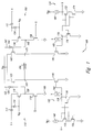
- FIG. 1 shows a bridge circuit 100 used to drive a coil 190 in a magnetic write head.
- the coil 190 is shown as an inductor, those skilled in the art will recognize that the coil behaves in a manner unlike an ideal inductor. This behavior is caused by such effects as. e.g ., parasitic capacitance of coil driving transistors, resistance effects in the coil 190 and other components of the bridge circuit 100, and various other factors.
- the bridge circuit 100 although described in this embodiment with reference to an inductive coil 190 for use in a magnetic write head, can be used to drive other components properly situated within the circuit 100, such as windings of a drive motor, an alternator used as a braking mechanism, or other compatible devices.
- the invention is not limited to the embodiment described herein nor the examples listed above, and is intended to be broad in scope.
- the coil 190 is driven by four bridge transistors including two upper transistors, 125 and 165, and two lower transistors, 145 and 185.
- the bridge circuit 100 is configured such that the upper transistor 125 and lower transistor 185 are both on hard when magnetic flux of a first direction is to be written by the coil 190 to the disk media. As seen in Figure 1, this causes the current flow from left to right across the coil 190. Conversely, when magnetic flux of a second direction is to be written to the disk media, the bridge circuit 100 turns on the upper transistor 165 and the lower transistor 145, thereby forcing the current from right to left across the coil 190.
- the upper transistors 125, 165 essentially serve as switching transistors, while the lower transistors 145, 185 serve as current control transistors dictating the magnitude of the current that flows through the coil 190.
- the individual driving circuits that drive the upper transistors 125, 165 and the lower transistors 145 and 185 are described below.
- a driving circuit 110 drives the upper transistor 125.
- a data signal X is coupled to one plate of a capacitor 112 and a data complement X is coupled to a gate of a transistor 118.
- a node 120 separates the transistor 118 from a transistor 116.
- the gate of the transistor 116 is coupled to a V DD voltage of, for example, 8 volts.
- the V DD voltage is also coupled to an anode of a diode 114, the cathode of which is coupled to a second plate of the capacitor 112 and to a source of the transistor 116.
- the anode of the diode 114 is coupled to the constant V DD voltage. Therefore, in a steady state, the plate of the capacitor 112 coupled to the cathode of the diode 114 is charged to a voltage of V DD minus the diode threshold voltage, typically around 0.7 volts. Therefore, if the V DD voltage is 8 volts, the second plate of the capacitor 112 charges to about 7.3 volts in the steady state.
- X in its steady state, has a value of 0 and is changing to 5 volts. This occurs when magnetic flux of the first direction is to be written by the coil 190.
- the second plate of the capacitor 112 rests at 7.3 volts.
- the capacitor 112 maintains the same voltage differential between the plates as it had previously, i.e ., 7.3 volts. Therefore, at the same time X changes from 0 to 5 volts, the second plate of the capacitor 112 escalates to approximately 12.3 volts.
- This voltage differential causes the transistor 116 to turn on and a voltage near 12 volts becomes present at the node 120.
- X changes from 0 volts to 5 volts X changes from 5 volts to 0 volts, turning the transistor 118 off, thereby isolating the node 120 from a reference voltage 105.
- a resistor 122 and diode 124 are coupled between the V DD voltage and the gate to the transistor 125. These components replenish any current leaking through the driving circuit 110 and thus keep the gate of transistor 125 above the V DD voltage less a diode drop voltage during the entire time the data signal X is at 5 volts.
- the driving circuit 150 is similar in configuration to the driving circuit 110, however, the signals are complemented. Thus, when one of the driving circuits 110, 150 is on, the other is off, and vice versa.
- the lower transistors 145 and 185 are also controlled by a symmetrical pair of driving circuits 130 and 170. Similar to the driving circuits described above, the driving circuit 130 is driven by data signals that are complementary to the driving circuit 170, so that one of the driving circuits 130, 170 is on while the other is off, and vice versa.
- a current source 140 is coupled in series to a transistor 132 and to a diode-connected transistor 134.
- the data signal X drives a gate of the transistor 132 as well as a gate of a transistor 136.
- the drain of the transistor 136 is coupled to a node 138, which couples the drain and gate of the diode-connected transistor 134 with a transistor 145 and a pull-up circuit 6 including a capacitor 142.
- the pull-up circuit 6 is driven by the data signal X .
- the transistor 136 turns on, pulling node 138 to ground. Because the data signal X is at 5 volts, the transistor 132 stays off. Additionally, any charge accumulated on the capacitor 142 is pulled to ground through the transistor 136. Therefore, when X changes from 0 to 5 volts, the lower transistor 145 is off.
- the driving circuit 170 that drives the gate of the lower transistor 185 is nearly identical to the driving circuit 130. However, it is driven by opposite signals. Specifically, it is the X data signal that drives the gates of transistors 176 and 172 and the data signal X that is coupled to a pull-up circuit 8.
- the node 178 couples the source of the transistor 172, the drain and gate of the transistor 174, the drain of the transistor 176, the pull-up circuit 8, and the gate for the transistor 185.
- the transistor 176 turns off, thus isolating the node 178 from the ground voltage.
- the transistor 172 begins conducting, and current flows from a current generator 180. The generated current that flows through the transistor 172 and the diode-connected transistor 174.
- the pull-up circuit 8 brings up the voltage at the node 178. This causes the transistor 185 to turn on hard.
- the upper transistor 125 and lower transistor 185 are both on hard. Thus, current flows through the transistor 125, across the transistor 190 from left to right and through the lower transistor 185 to ground.
- the other transistors, 145 and 165 are both off during this time.
- the data signal X changes from 5 volts to 0 volts
- the reverse is true. That is, the upper transistor 165 turns on, allowing current to flow from right to left through the coil 190 and through the transistor 145 to ground.
- Overshoot is a condition where greater than normal current is provided to the coil of an H-bridge circuit at the beginning of a data transmission to initiate a quick flux reversal in the coil. This allows the magnetic field surrounding the coil to switch directions faster than in a typical H-bridge circuit. Since the flux can reverse faster in coil having overshoot, a greater amount of data can be written to the recording media than with a conventional H-bridge circuit. Too much overshoot can be detrimental, however, because the excess current can overwrite data intended to be written to the recording media. Thus it is desirable to have an H-bridge circuit with a "programmable" overshoot, in order to exactly control the amount of current flowing through the coil at a time.
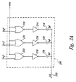
- Figure 2A shows a programmable circuit 200 that can be used as the pull-up circuits 6 and 8 of Figure 1.
- the programmable circuit 200 include three NOR gates, 210, 220 and 230. Of course, a greater or fewer number of gates could be used, the number of gates being determined by, among other factors, the amount of pull-up boost needed and the granularity of the boost, as later discussed.
- Each of the NOR gates 210, 220, and 230 has a pair of inputs, one for a respective programming signal, b0*, b1*,b2*, and one for a data signal common to all of the NOR gates within the programmable circuit 200.
- the output from the NOR gate 210 is coupled to an inverter 216, the output of which is coupled to a capacitor 218.
- the output from the NOR gate 220 is coupled to an inverter 226 which has its output coupled to a capacitor 228, and the output of the NOR gate 230 is coupled to an inverter 236 which has its output coupled to a capacitor 238.
- An OR gate could be used instead of a NOR gate followed by an inverter, however, in a preferred embodiment, the size of the transistors making the inverter are chosen to be large enough to drive the coupled capacitor.
- a pull-up voltage, such as 5 volts, placed on a first one of the plates of a capacitor will tend to pull the second plate of the capacitor to a voltage near that of the first plate.
- the rate at which the voltage of the second plate tends toward the voltage of the first plate is a function of the capacitance value of the capacitor, among other factors.
- a pull-up voltage output from any of the inverters will tend to pull up an output 250 of the programming circuit 200 toward the pull-up voltage of the inverter, for example, 5 volts.
- the rate at which the output 250 is pulled up toward 5 volts is related to the total capacitance of the capacitors 218, 228 and 238 that are coupled to the 5 volt source, as well as other factors.
- the signals b0*, b1*, and b2* are selected to couple at least one, and as many as all of the capacitors 218, 228, and 238 to the output 250. Higher values of total capacitance coupled to the output 250 will allow it to be pulled up toward the pull-up voltage faster than if lesser capacitance is applied.
- the capacitance values for the capacitors 218, 228, and 238 are binary weighted, so that the capacitor 228 has twice as much capacitance as the capacitor 218, and has one-half the capacitance as the capacitor 238.
- Figure 2B is a chart showing the output of one of the NOR gates, for instance the NOR gate 210, and its corresponding inverter 216.
- the chart shows that when the b0* input to the NOR gate is 1, the NOR gate output is always 0, and the inverter output signal is always 1, no matter what value the data input has. Therefore, the signal b0* must be 0 to enable the NOR gate.
- the output of the NOR gate is determined solely by the state of the data signal.
- the output of the NOR gate is 1 when the data signal is 0 and the output is 1 when the data signal is 0.
- the inverter output is 1, and when the output of the NOR gate is 1, the inverter output is 0.
- the NOR gates 210, 220, and 230 are selectively enabled to capacitively couple the output 250 to a pull-up voltage so that when the data signal goes from 0 volts to 5 volts, the output 250 is pulled up toward the pull-up voltage volts at the desired rate.
- Figure 2C is a chart showing the total capacitance coupled between the output 250 and the pull-up voltage, depending on which of the NOR gates are enabled. Shown in Figure 2C are eight different possibilities of the output from the inverters 216, 216 and 226 as well as the total capacitance coupled to the output 250.
- the capacitor 218 has a value of 2pF, the capacitor 228, 4pF and the capacitor 238, 8pF. Although other capacitance values are possible, in a preferred embodiment it is desirable to keep the capacitors in a binary-weighted relationship.
- the output of each of the inverters 216, 226, and 236 also changes towards a high value.
- the output of the inverters is applied to the first plate of each of the transistors 218, 228 and 238, the second plate of which is coupled to the output 250, which in this example is also node 178.
- the pull-up voltage begins pulling the second plate of the capacitors towards a high value.
- the capacitors 218, 228 and 238 appear as a short circuit.
- the voltage on the first plate is transferred immediately to the second plate.
- the value on the output line 250 and thus node 178 follows the output of the enabled inverters 216, 226, 236.
- the gate of 185 goes high, turning on transistor 185.
- the transistor 185 thus receives a high value transient pulse as a turn-on signal.
- the output of the inverters 216, etc. go towards five volts. It can, of course be selected to go to desired voltage, such as 8 volts, 3 volts, etc., at a desired rate.
- NOR gate 210 for capacitor 218, is enabled.
- the high voltage transient signal from boost circuit 182 is reduced as a programmable rate, depending on the selection of which gates are enabled.
- This secondary factor is the diode-coupled transistor 174, which operates as a voltage divider with the transistor 172.
- the diode-coupled transistor 174 will pull the node 178 down toward a static voltage of a value based on the threshold of 174 and 172 and currents from 180. Usually it will be midrange voltage of, for instance, slightly over 2 volts.
- the programmable circuit 200 enables the voltage applied to the gate of the transistor 185 to begin at 0, progress toward 5 volts and reach between 3 1/2-4 1/2 volts before it begins to be pulled down to the stable 2.2 volts as set by the divider circuit of transistors 174 and 172.
- This programmable circuit 200 not only allows the voltage on the gate of the transistor 185 to come up faster than it would have had the programmable circuit 200 not been present, it also holds this gate voltage on the gate of the transistor 185 for a time before being drained.
- the maximum pull-up voltage as well as the rate at which the pull-up voltage is drained away is selectable by the disk drive manufacturer.
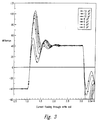
- Figure 3 shows simulation results from the embodiment of the invention described with respect to Figures 1 and 2.
- the graph shows current flowing through the coil 190, in milliamps during the time data is to be written to the magnetic media.
- seven separate waveforms are shown, corresponding to the seven allowable program settings of the programmable circuit 200 shown in Figure 2C. Since the bridge circuit 100 will not work unless external capacitance is applied to the output 250 of the programmable circuit 200, the waveform where no capacitance is added has been omitted in the graph. The other seven possibilities are shown in Figure 3.
- the capacitance values for the waveforms shown on Figure 3 maintain a logical progression.
- the waveform showing the lowest peak current (41 mA) is the condition where only 2pF is provided to the output 250 of the programmable circuit 200. Since the output 250 is directly coupled to one of the lower transistors 145 or 185 ( Figure 1), having the low capacitance value means it cannot turn the respective transistor on very hard and consequently little peak current flows through the coil 190.
- the waveform showing the highest peak current (112 mA) is the condition where all of the NOR gates 210, 220, and 230 are enabled, coupling 14pF to the output 250. This causes the output 250 to pull up hard when the data input of the programmable circuit 200 transitions to 1, thus turning on the respective lower transistor 145, 185 and sending a high peak current through the coil 190.
- the coil 190 does not behave as a pure inductor, however, but more like an RC circuit, due to the parasitic capacitance of the upper transistors 125, 165 and the lower transistors 145 and 185. This causes the current sent through the coil 190 to oscillate before it eventually becomes fixed.
- the value to which it finally fixes is unrelated to the additional capacitance added to bridge circuit 100 by the programmable circuit 200, as proven by all of the waveforms in Figure 3 settling at the same final value. Instead, as discussed above, this stable voltage value is determined by the resistance of the diode-coupled transistors 134 and 174.
- the disk drive is tested with various total capacitance values until an optimum value is determined. Then the proper codes that cause programming signals to be generated are permanently stored in a non-volatile memory, such as an EPROM or EEPROM. When the disk drive is turned on, these signals are fed to the programmable circuit 200, which enables one or more of the NOR gates.
- the programmable circuit 200 is programmed at the time a disk drive is initialized, usually when it is first powered, according to set parameters determined at manufacture. The optimum value of applied capacitance to the output 250 of the programmable circuit 200 may change as the disk drive 400 ages.
- this optimum capacitance value can be updated throughout the life of the disk drive.
- the program may direct circuitry within the disk drive to measure the output of the write coil 190. A new optimum capacitance value can be selected and restored to the non-volatile memory.
- This diagnostic program could be run as often as the operator chooses. Greater detail of the programming the programmable circuit 200 is provided with the description accompanying Figure 4.
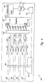
- Figure 4 is a diagram of a disk drive that can be used to store data in, for instance, a computer (not shown).
- the drive 400 includes a motor 402 for rotating a spindle 404 which in turn rotates platters of storage media 406. Although four platters 406 are shown in Figure 4, more or fewer platters could be used as is known in the art a motor controller 420 receives signals from a RAM interface 422 and uses those signals to control the motor 402.
- the drive 400 also contains an actuator 408 that provides support for a number of support arms 410.
- the number of support arms 410 will generally be twice the number of platters 406 contained in the disk drive 400, although more or fewer support arms 410 could be used.
- a write head 412 used to write data to a respective planer 406 and a read head 414 used to read data from the platter.
- the write head 412 and read head 414 may be embodied in one read/write head (not shown).
- the platters 406 have a magnetic storage medium on both sides, thus one read head 412 and one write head 414 will be positioned near each side of every planer 406. In operation, the heads 412, 414 float on a cushion of air very close to the spinning platters 406.
- the microprocessor 430 receives signals from the RAM interface unit 422.
- the interface unit 422 receives control and data signals from the computer system (not shown).
- the interface unit 422 is typically coupled to the computer system via a bus such as a PCI or SCSI bus (not shown), as is well known in the art.
- the microprocessor 430 is also coupled via a serial interface 440 to a preamplifier 444.
- the preamplifier 444 contains a bridge circuit 100 of Figure 1, including the programmable circuit 200 depicted in Figure 2 for each of the write heads in the drive 400, as well as other circuitry 434, known in the art.
- the preamplifier 444 is coupled to each write head 412 by a communication path 448.
- the drive 400 When the drive 400 is manufactured, the drive is tested to see which configuration, ( Figure 2C) of the programmable circuit 200 provides the optimum results for proper data transfer. This configuration is then stored into the ROM of the microprocessor 430.
- the codes stored in the ROM memory of the microprocessor 430 are sent along the serial bus 444 to the preamplifier 444, enabling the proper NOR gates of the programmable circuit 200.
- the heads 412 of the drive 400 operate at their optimum levels as data is written to the drive.
Landscapes
- Digital Magnetic Recording (AREA)
Applications Claiming Priority (2)
| Application Number | Priority Date | Filing Date | Title |
|---|---|---|---|
| US258100 | 1999-02-25 | ||
| US09/258,100 US6198335B1 (en) | 1999-02-25 | 1999-02-25 | Method and apparatus to drive the coil of a magnetic write head |
Publications (2)
| Publication Number | Publication Date |
|---|---|
| EP1032131A2 true EP1032131A2 (fr) | 2000-08-30 |
| EP1032131A3 EP1032131A3 (fr) | 2004-11-10 |
Family
ID=22979099
Family Applications (1)
| Application Number | Title | Priority Date | Filing Date |
|---|---|---|---|
| EP00301254A Withdrawn EP1032131A3 (fr) | 1999-02-25 | 2000-02-17 | Appareil et méthode pour attaquer la bobine d'une tête magnétique d'écriture |
Country Status (3)
| Country | Link |
|---|---|
| US (1) | US6198335B1 (fr) |
| EP (1) | EP1032131A3 (fr) |
| JP (1) | JP2000251209A (fr) |
Cited By (1)
| Publication number | Priority date | Publication date | Assignee | Title |
|---|---|---|---|---|
| DE10101074A1 (de) * | 2001-01-11 | 2002-08-01 | Infineon Technologies Ag | Schaltungsanordnung zur Ansteuerung einer Last |
Families Citing this family (10)
| Publication number | Priority date | Publication date | Assignee | Title |
|---|---|---|---|---|
| KR100468778B1 (ko) | 2002-12-13 | 2005-01-29 | 삼성전자주식회사 | 하드디스크 드라이브의 기록 전류 최적화 방법 및 기록밀도 설정 방법 |
| JP4680013B2 (ja) * | 2005-09-06 | 2011-05-11 | 三洋電機株式会社 | モータ駆動回路 |
| US7245536B1 (en) * | 2006-02-15 | 2007-07-17 | Catalyst Semiconductor, Inc. | Precision non-volatile CMOS reference circuit |
| US7817401B2 (en) | 2007-05-15 | 2010-10-19 | Extremely Ingenious Engineering LLC | Solid state tesla coil suit |
| WO2008156814A1 (fr) * | 2007-06-20 | 2008-12-24 | Extremely Ingenious Engineering, Llc | Système et procédé pour utiliser un résonateur supraconducteur à température élevée à noyau sous vide |
| US7960867B2 (en) * | 2007-11-27 | 2011-06-14 | Extremely Ingenious Engineering | Methods and systems for wireless energy and data transmission |
| US8411390B2 (en) * | 2009-10-16 | 2013-04-02 | Hitachi Global Storage Technologies Netherlands B.V. | Integrated half coil structure for write assist of high coercivity media |
| US8638527B2 (en) * | 2009-10-16 | 2014-01-28 | Hitachi Global Storage Technologies Netherlands B.V. | Signaling method and apparatus for write assist of high coercivity media using integrated half coil |
| US8493146B2 (en) * | 2011-03-10 | 2013-07-23 | Silicon Laboratories Inc. | Amplifier using fast discharging reference |
| US8508298B2 (en) * | 2011-03-10 | 2013-08-13 | Silicon Laboratories Inc. | Amplifier using master-slave control scheme |
Family Cites Families (11)
| Publication number | Priority date | Publication date | Assignee | Title |
|---|---|---|---|---|
| JPH0833974B2 (ja) * | 1987-08-19 | 1996-03-29 | ソニー株式会社 | 磁気ヘッド駆動回路 |
| IT1251205B (it) * | 1991-09-18 | 1995-05-04 | St Microelectronics Srl | Circuito a ponte ad h con protezione contro la conduzione incrociata durante l'inversione della corrente nel carico. |
| JP2755047B2 (ja) * | 1992-06-24 | 1998-05-20 | 日本電気株式会社 | 昇圧電位発生回路 |
| US5331479A (en) * | 1993-02-01 | 1994-07-19 | Seagate Technology, Inc. | Capacitor assisted low voltage write circuit |
| US5534819A (en) * | 1995-04-13 | 1996-07-09 | Motorola, Inc. | Circuit and method for reducing voltage error when charging and discharging a variable capacitor through a switch |
| FR2742280A1 (fr) * | 1995-12-06 | 1997-06-13 | Philips Electronics Nv | Circuit de commutation de courant dans une charge principalement inductive |
| US5990640A (en) * | 1996-03-29 | 1999-11-23 | Aim Controls, Inc. | Motor control apparatus |
| JP3665419B2 (ja) * | 1996-05-02 | 2005-06-29 | 新電元工業株式会社 | 誘導性負荷駆動方法、及びhブリッジ回路制御装置 |
| US5869988A (en) * | 1997-03-25 | 1999-02-09 | Marvell Technology Group, Ltd. | High speed write driver for inductive heads |
| US6011423A (en) * | 1997-05-23 | 2000-01-04 | International Business Machines Corporation | Virtual voltage power supply |
| US6366421B2 (en) * | 1998-12-17 | 2002-04-02 | Texas Instruments Incorporated | Adjustable writer overshoot for a hard disk drive write head |
-
1999
- 1999-02-25 US US09/258,100 patent/US6198335B1/en not_active Expired - Lifetime
-
2000
- 2000-02-17 EP EP00301254A patent/EP1032131A3/fr not_active Withdrawn
- 2000-02-25 JP JP2000048610A patent/JP2000251209A/ja active Pending
Cited By (2)
| Publication number | Priority date | Publication date | Assignee | Title |
|---|---|---|---|---|
| DE10101074A1 (de) * | 2001-01-11 | 2002-08-01 | Infineon Technologies Ag | Schaltungsanordnung zur Ansteuerung einer Last |
| DE10101074B4 (de) * | 2001-01-11 | 2005-05-19 | Infineon Technologies Ag | Schaltungsanordnung zur Ansteuerung einer Last |
Also Published As
| Publication number | Publication date |
|---|---|
| JP2000251209A (ja) | 2000-09-14 |
| EP1032131A3 (fr) | 2004-11-10 |
| US6198335B1 (en) | 2001-03-06 |
Similar Documents
| Publication | Publication Date | Title |
|---|---|---|
| US6052017A (en) | Method and circuit for enabling rapid flux reversal in the coil of a write head associated with a computer disk drive, or the like | |
| US6198335B1 (en) | Method and apparatus to drive the coil of a magnetic write head | |
| US7474553B2 (en) | Device writing to a plurality of rows in a memory matrix simultaneously | |
| US6970316B2 (en) | Write head driver circuit and method for writing to a memory disk | |
| US6831800B2 (en) | Boost system and method to facilitate driving a load | |
| US6456148B2 (en) | Circuit and method for writing to a memory disk | |
| US6259305B1 (en) | Method and apparatus to drive the coil of a magnetic write head | |
| US6366421B2 (en) | Adjustable writer overshoot for a hard disk drive write head | |
| EP1113423B1 (fr) | Améliorations à des entraînements pour disques | |
| US6512645B1 (en) | Circuit and method for writing to a memory disk with a boosted voltage | |
| US6128146A (en) | Undershoot active damping circuit for write drivers | |
| EP1187102A2 (fr) | Méthode pour l'enregistrement différentiel sur un disque de mémoire | |
| US7688536B2 (en) | Variable power write driver circuit | |
| KR20200144495A (ko) | 전압 발생 회로, 반도체 스토리지 디바이스 및 그 비트 라인 충전 방법 | |
| JP2001211686A (ja) | アクテイブ減衰回路 | |
| US6580575B1 (en) | Process and temperature resistant active damping circuit for inductive write drivers | |
| US6297919B1 (en) | Write head with switchable impedance and method for operating same | |
| US6580238B2 (en) | Motor driver | |
| US6867936B2 (en) | Driving circuit for a magnetic head and magnetic recording apparatus | |
| JP2001057036A (ja) | 磁気ディスク駆動装置用の信号処理回路装置及び磁気ディスク駆動装置 |
Legal Events
| Date | Code | Title | Description |
|---|---|---|---|
| PUAI | Public reference made under article 153(3) epc to a published international application that has entered the european phase |
Free format text: ORIGINAL CODE: 0009012 |
|
| AK | Designated contracting states |
Kind code of ref document: A2 Designated state(s): AT BE CH CY DE DK ES FI FR GB GR IE IT LI LU MC NL PT SE |
|
| AX | Request for extension of the european patent |
Free format text: AL;LT;LV;MK;RO;SI |
|
| PUAL | Search report despatched |
Free format text: ORIGINAL CODE: 0009013 |
|
| AK | Designated contracting states |
Kind code of ref document: A3 Designated state(s): AT BE CH CY DE DK ES FI FR GB GR IE IT LI LU MC NL PT SE |
|
| AX | Request for extension of the european patent |
Extension state: AL LT LV MK RO SI |
|
| RIC1 | Information provided on ipc code assigned before grant |
Ipc: 7G 11B 5/02 B Ipc: 7G 11B 5/012 B Ipc: 7G 11B 19/02 B Ipc: 7G 11B 5/09 B Ipc: 7H 03K 17/64 A |
|
| 17P | Request for examination filed |
Effective date: 20050419 |
|
| AKX | Designation fees paid |
Designated state(s): DE FR GB IT |
|
| GRAP | Despatch of communication of intention to grant a patent |
Free format text: ORIGINAL CODE: EPIDOSNIGR1 |
|
| STAA | Information on the status of an ep patent application or granted ep patent |
Free format text: STATUS: THE APPLICATION IS DEEMED TO BE WITHDRAWN |
|
| 18D | Application deemed to be withdrawn |
Effective date: 20090721 |