EP1032883B1 - Wiederabtastungssystem für datenverarbeitung - Google Patents
Wiederabtastungssystem für datenverarbeitungInfo
- Publication number
- EP1032883B1 EP1032883B1 EP98957839A EP98957839A EP1032883B1 EP 1032883 B1 EP1032883 B1 EP 1032883B1 EP 98957839 A EP98957839 A EP 98957839A EP 98957839 A EP98957839 A EP 98957839A EP 1032883 B1 EP1032883 B1 EP 1032883B1
- Authority
- EP
- European Patent Office
- Prior art keywords
- data
- address
- memory
- registers
- cache
- Prior art date
- Legal status (The legal status is an assumption and is not a legal conclusion. Google has not performed a legal analysis and makes no representation as to the accuracy of the status listed.)
- Expired - Lifetime
Links
Images



Classifications
-
- G—PHYSICS
- G06—COMPUTING OR CALCULATING; COUNTING
- G06T—IMAGE DATA PROCESSING OR GENERATION, IN GENERAL
- G06T3/00—Geometric image transformations in the plane of the image
- G06T3/40—Scaling of whole images or parts thereof, e.g. expanding or contracting
- G06T3/4007—Scaling of whole images or parts thereof, e.g. expanding or contracting based on interpolation, e.g. bilinear interpolation
Definitions
- This invention relates to data processing systems and more particularly, to a data resampler and data resampling method for a data processing system for processing a stream of data containing logically adjacent or related data samples such as in a machine vision system.
- Machine vision systems (or other systems processing 2-dimensional data) often need to resample images to adjust scale, rotation, or other distortions in the original data prior to further processing.
- This operation is referred to herein as warping.
- a well known computationally efficient technique uses bilinear interpolation for this purpose. This algorithm reads four neighboring samples surrounding the sub-sample location in the source image to be rendered (2x2 aperture).
- the hardware described is easily extended to higher-order interpolation kernel techniques which nonetheless fetch a fixed number of surrounding samples.
- the location to be rendered may be determined by a number of well-known techniques.
- One technique suitable for efficient hardware implementation iteratively computes horizontal and vertical difference equations which cause the sampling point to move through the source image at successive sub-sample points. In the current embodiment, these difference equations compute a linear path. This is commonly known as a linear DDA (Digital Differential Analyzer).
- Various other techniques such as higher order DDAs or a data structure containing pre-computed sub-sample points to be rendered could also benefit from the techniques to be described.
- a second problem occurs in the rendering process due to the nature of burst-mode memories (e.g. SDRAM, SGRAM). This is because all four neighboring pixels which must be fetched on each step do not generally lie on the same memory row. This can degrade performance as memory addressing repeatedly crosses (thrashes) memory row boundaries during the fetch process.
- burst-mode memories e.g. SDRAM, SGRAM
- JP 08 212 357 A One example of a prior art method and apparatus for resampling and interpolating images is disclosed in JP 08 212 357 A in which a single mapping address generator generates coordinates of texture that are provided to an interpolator.
- the current invention addresses the speed problem of the prior art by making a continuous stream of new parameters available to the DDA hardware.
- the current invention uses three mechanisms to address the memory thrashing problem.
- address and data caches are employed for re-using pixels which may already have been fetched in a previous step.
- the invention exploits SDRAM/SGRAM architecture by placing odd and even image rows in opposite internal banks and pre-activating the next bank address to anticipate the next row address required.
- the FIFO technique described in co-pending Patent No. 6,208,772 is extended to mitigate the address to data latency of the burst-mode memories.
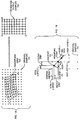
- FIG. 1A is an overview of a resampling process according to the present invention.
- a 2-dimensional array of adjacent image data samples 701 is stored in memory. Typically these are taken directly from the data source.
- the resampling grid 702 represents points at which samples are to be rendered. For each point in the resampling grid 702, a result is generated (rendered) and stored in the 2-dimensional rendered output sample array 703.
- the resampling grid or array 702 consists of a series of straight line segments. These segments can piecewise approximate any type of warp distortion.
- Each rendering sequence involves moving along one of these lines at equally spaced, arbitrary sized steps. Thus, in the illustration, moving along the six resampling grid steps from A to B generates the seven rendered output values from A' though B'.
- Fig. 1B details the process of rendering one of the linear segments (e.g. A to B).
- the initial sampling point 704 (e.g. A) is represented as an initial whole pixel address in the original sample array 701, and x and y subpixel offsets from that address.
- a new sampling point is computed by adding the delta-x and delta-y steps to the present x-y position with full subpixel precision.
- Each sampling location can be expressed as a pair of mixed fractions for X and Y.
- the integer parts representing pixel address and the fractional parts representing subpixel fractions. Interpolation is required except when the sampling location is exactly at an original sample point (both fractional parts are zero).
- Bilinear interpolation involves fetching the four pixels surrounding the sampling point. Note that movement in the Y direction involves the "stride" constant (the distance between the rows in the original sample array 701. The rendered output result is computed by considering all four neighboring pixels and the inverse distance of the sampling point from each of the four original samples.
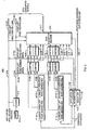
- the DDA unit 401 Fig. 2, generates a corner address and a set of interpolation coefficients for each sample to be rendered.
- a linear DDA requires the following parameters which are loaded into working parameter registers 401a:
- these parameters are loaded into DDA unit registers prior to each operation.
- the DDA unit 401 generates an interpolation corner address 503.
- the fetch unit 402 uses the generated interpolation corner address 503 to generate four source addresses 505 of samples to be fetched from the source array via memory subsystem 0 120a.
- the DDA unit 401 also generates a set of interpolation fractions 507 (x and y fractions) for each point to be rendered. Because of memory read latency (as described elsewhere herein), there is some delay before valid data is available.
- the interpolation fractions 507 are held in a first, first-in, first-out memory 90d (FIFO Q), permitting the DDA unit 401 and fetch unit 402 to continue to operate during the memory read latency period.
- An interpolation unit 403 receives pixel data 509 from a second FIFO memory unit, FIFO A 90a and interpolation fractions 507 from FIFO Q 90d. The interpolation unit then computes the rendered result pixels, assembles them into memory words 17, and outputs the words to the destination memory subsystem 1 120b via a third FIFO memory unit, FIFO C 90c.
- the destination address 511 is supplied by address generator C 41c.
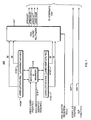
- parameter registers are double-buffered as shown in Figure 3B.
- Two sets of registers 420a-420b are used. During a warping operation, one set of registers 420a/420b supplies the working values to the DDA circuit while the other is available to be loaded from data buffer 102 under control of sequencer 421. In this way, no parameter loading delay need be encountered when one DDA run terminates and another starts.
- an address cache 404 and a data cache 405 are added as shown in Figure 4.
- the width of FIFO Q 90d is also increased to carry a data descriptor 513 along with each set of interpolation fractions 507.
- the data cache 405 consists of two cache lines (register sets) each holding two four (4) pixel memory words 17.
- the contents of the data cache registers represent an 8x2 pixel neighborhood.
- the address cache 404 has two cache lines comprising upper and lower cache lines. Each cache line is comprised of two address registers. Each address register, when valid, holds the address of a word in source memory 120a. Data from the two words thus points to eventually become the contents of the corresponding data cache 405 cache line.
- the present invention is described in connection with four (4) pixel words per memory word, this is not a limitation of the present invention as it also applies to wider or narrower memory words as will be appreciated by those skilled in the art.
- Address cache 404 computes the four required addresses based on the incoming DDA corner address. It then compares these with all valid addresses currently resident in the address cache 404 and determines if any new data needs to be fetched from memory. It then instructs the fetch unit 402 to supply the required addresses to the source memory subsystem 120a. At the same time, it encodes and outputs a data descriptor 513 containing instructions for the data cache unit 405. The data descriptor specifies how the data cache 405 is to update its registers from FIFO A 90a if required, and how to form the required interpolation neighborhood once its registers contain valid data.
- two memory words are always fetched whenever a cache line is re-filled, exploiting the efficient burst mode capability of SDRAM/SGRAM.
- the data descriptor 513 can also instruct the data cache 405 to load the upper cache line from the lower cache line or vice versa.
- the address cache 404 can reload the upper from the lower address cache line or vice versa as the addresses are processed.
- the required four pixels are supplied to the interpolation unit 403 using information from the data descriptor 513, along with the interpolation fractions 507 from FIFO Q 90d.
- the operation of the address cache 404 is detailed in Figure 5.
- the lower-left pixel address 516 is generated by adding the stride 514 to the corner pixel (upper-left) address 515 using adder 410.
- the most significant bits of these addresses represent a memory address containing the desired pixel. In the present example, there are four pixels in each memory word 17, and there are 26 bits of pixel address corresponding to 24 bits of memory address 515a and 516a and 2 bits of pixel position 515b and 516b within the memory word.
- the first line comprises registers 411a and 411b.
- the second cache line includes registers 411c and 411d.
- one register for example the left registers
- 411a and 411c holds the address of the memory word containing the left pixel
- one register for example the right registers
- 411b and 411d holds the address of the next word. This means that both the left and right pixels are contained within the two words pointed to by the left and right address registers. This is illustrated by the examples in Figure 6.
- the p00 2x2 neighborhood 602 lies entirely within the cache.
- both cache lines must be updated.
- four new memory words are fetched in this case. Note that words 01 605 and 11, 607 could have been reused. This was not deemed necessary due to the high SDRAM/SGRAM burst bandwidth.
- the lower cache line (words 10, 603 and 11, 607), are transferred to the upper cache line (words 00, 601 and 01 605), and the lower registers 411c and 411d are updated from the incoming lower-left word address 516a. Whenever a cache line is updated, the incrementer 412 generates the right address or addresses.
- Data descriptor encoder 414 generates a data cache update descriptor 517, which enters FIFO Q (90d of Figure 3A) along with the pixel location bits 515b and 516b as data descriptor 513, along with the interpolation fractions 507.
- the encoder 414 also instructs the incrementer 412 to update the address cache working registers 411a-411d using data switch 418 and sequencer 419.
- the sequencer 417 also requests words to be fetched from memory via the fetch unit 402, via a fetch signal 518.
- the data descriptor 517 includes the sign of the vertical DDA (y-sign) 519, Fig. 5. This determines the order in which the fetch unit will request and the data cache will receive data from the upper and lower memory rows.
- the y-sign 519 also instructs the source memory controller (40 in Figure 5 of co-pending US Patent
- the encoder 414 also receives a clip input signal 520 from the DDA unit 401. When this is asserted, the DDA unit has determined that at least one source address is invalid. In this case, no data is fetched and the data cache forwards the signal to the interpolate unit 403 which outputs a default value to the result-C bus 17 for the corresponding pixel.
- the data cache 405, Fig. 7, has four (4) working registers 415a-415d each holding a memory word. Pairs of registers, 415a/415b and 415c/415d left and right, each comprise a data cache line holding eight pixels.
- the data switch and sequencer 416 updates working registers 415a-415d based on the data descriptor 513 from the output of FIFO Q 90d. When working register update is required, data is taken from FIFO A 90a.
- the data switch 416 can also move data between the upper and lower cache lines when required.
- the data descriptor 513 insures that the sequence of updates corresponds to the sequence of addresses issued to the source data memory subsystem 120a.
- Pixel output multiplexer 417 selects the four pixels forming the required 2x2 neighborhood for interpolation using the corresponding FIFO Q pixel select fields.
- the corresponding interpolation fractions 507 from the FIFO Q are passed directly to the interpolation unit 403 which forms four coefficients based on the interpolation fractions; multiplies each by the corresponding pixel value to provide four products; sums the four products; and normalizes the result, producing the rendered pixel value.
- clip 520 from the DDA 401 is asserted, the interpolation unit outputs a default value.
- the rendered pixel output values are packed into a memory word and output to the destination bus. In the current embodiment, four pixels are rendered for each memory word written out.
- the present invention provides a novel data resampler for processing logically adjacent data samples.
Landscapes
- Physics & Mathematics (AREA)
- General Physics & Mathematics (AREA)
- Engineering & Computer Science (AREA)
- Theoretical Computer Science (AREA)
- Image Processing (AREA)
- Image Input (AREA)
- Separation By Low-Temperature Treatments (AREA)
- Saccharide Compounds (AREA)
- Preparation Of Compounds By Using Micro-Organisms (AREA)
- Measurement Of Velocity Or Position Using Acoustic Or Ultrasonic Waves (AREA)
Claims (24)
- Datenwiederabtaster für ein Datenverarbeitungssystem, das logisch benachbarte Datenabtastwerte (701) verarbeitet, wobei der Datenabtaster folgendes umfaßt:ein Speichersubsystem (120a) zum Speichern mindestens einer Vielzahl von wiederzugebenden Datenabtastwerten (701);einen digitalen Differenzanalysator (DDA) (401), der auf DDA-Parametermengen reagiert, zum Erzeugen einer Interpolationseckenadresse (503) für die wiederzugebende Vielzahl von Datenabtastwerten und außerdem zum Erzeugen einer Menge von Interpolationsbrüchen (507);eine Abrufeinheit (402) zum Empfangen der erzeugten Interpolationseckenadresse (503) und zum Erzeugen von vier Quellenadressen (505) von aus dem Speichersubsystem (120a) abzurufenden Datenabtastwerten;dadurch gekennzeichnet, daß der Datenabtaster folgendes umfaßt:einen ersten FIFO-Speicher (90d) zum Halten der Interpolationsbrüche (507) und zur Ermöglichung eines fortgesetzten Betriebes des DDA (401) und der Abrufeinheit (402) während Speicherleselatenzperioden;einen zweiten FIFO-Speicher (90a) zum Halten von Pixeldaten;einen ersten Adressengenerator (41c);einen Adressen-Cache (404) und einen Daten-Cache (405), wobei der Daten-Cache (405) mindestens zwei Cache-Linien umfaßt, die jeweils zwei Speicherwörter halten, und wobei der Adressen-Cache mindestens zwei Cache-Linien umfaßt, die jeweils aus zwei Adressenregistern bestehen, wobei jedes Adressenregister zum Halten einer Adresse eines Worts (17) in dem Speichersubsystem (120a) dient; undeine Interpolationseinheit (403) zum Empfangen von Pixeldaten (509) aus dem zweiten FIFO-Speicher (90a) und von Interpolationsbrüchen (507) aus dem ersten FIFO-Speicher (90d) zum Berechnen wiedergegebener Ergebnispixel (703), zum Zusammenstellen der Ergebnispixel zu Speicherwörtern (17) und zum Ausgeben der Speicherwörter (17) an eine Zielspeicheradresse (511), die von dem Adressengenerator (41c) in einem Zielspeichersubsystem (120b) über einen dritten FIFO (90c) zugeführt wird.
- Datenwiederabtaster nach Anspruch 1, ferner umfassend:einen Datenpuffer (102) zum Halten von DDA-Parametermengen in DDA-Parameterregistern (401a), wobei die DDA-Parametermengen immer dann, wenn der Datenpuffer (102) leer ist, aus dem Speichersubsystem (120a) abgerufen werden; undeinen zweiten Adressengenerator zum Liefern von Speichersubsystemadressen an das Speichersubsystem (120a) für aus dem Speichersubsystem (120a) abzurufende DDA-Parametermengen.
- Datenwiederabtaster nach Anspruch 2, ferner mit einem vierten FIFO zum Erweitern der Kapazität des Datenpuffers (102) und wobei die DDA-Parameterregister (401a) doppelt gepuffert sind und zwei Mengen von Registern (420a, 420b) umfassen, wobei eine erste Menge davon Arbeitswerte an den DDA (401) liefert und eine zweite Menge davon für ein Laden aus dem vierten FIFO unter der Kontrolle eines Sequenzers (421) verfügbar ist, um Parameterladeverzögerungen zu beseitigen.
- Datenwiederabtaster nach einem der vorhergehenden Ansprüche, wobei die Breite des ersten FIFO (90d) vergrößert ist, um zusammen mit jeder Menge von Interpolationsbrtichen (507) einen Datendeskriptor (513) zu führen.
- Datenwiederabtaster nach einem der vorhergehenden Ansprüche, ferner mit einem Addierer (410) zum Erzeugen einer unteren linken Pixeladresse (516) aus einer oberen linken Pixeladresse (515) durch Addieren eines Schritts (514) zu der oberen linken Pixeladresse (515).
- Datenwiederabtaster nach einem der vorhergehenden Ansprüche, ferner mit vier Arbeitsadressenregistern (411a - 411d), die als zwei Addressencache-Linien jeweils mit einem linken und einem rechten Register zum Halten von Adressen von Speicherwörtern (17) organisiert sind, wobei in jeder Linie das linke Register die Adresse des Speicherworts (17), das das linke Pixel enthält und das rechte Register die Adresse des nächsten Worts (17) enthält.
- Datenwiederabtaster nach Anspruch 6, ferner mit einem Inkrementierer (412) zum Erzeugen von korrekten Speicheradressen immer dann, wenn eine Cache-Linie aktualisiert wird.
- Datenwiederabtaster nach Anspruch 7, ferner mit mindestens einem Komparator (413a - 413h) zum Vergleichen der Speicheradressen des oberen linken (515) und des unteren linken (516) Pixel mit dem Inhalt aller vier Arbeitsadressenregister (411a - 411d) .
- Datenwiederabtaster nach Anspruch 8, ferner mit einem Datendeskriptorcodierer (414) und einem Datenschalter (418) und -sequenzer (419), wobei der Deskriptorcodierer (414) zum Erzeugen eines Daten-Cache-Aktualisierungsdeskriptors (517) und zum Anweisen des Datenschalters und -sequenzers zum Aktualisieren der Adressenarbeitsregister (441a - 411d) dient, und zum Anfordern von aus dem Speicher über die Abrufeinheit (402) abzurufenden Wörtern.
- Datenwiederabtaster nach Anspruch 1, wobei der Daten-Cache (405) vier Arbeitsregister (441a - 411d) umfaßt, die jeweils ein Speicherwort (17) halten, wobei die Register zu linken und rechten Paaren angeordnet sind, wobei jedes Paar eine Daten-Cache-Linie umfaßt, die zweimal die Anzahl von Pixeln pro Speicherwort hält.
- Datenwiederabtaster nach Anspruch 10, ferner mit einem zweiten Datenschalter und -sequenzer, der Arbeitsregister auf der Basis eines Datendeskriptors (513) aus der Ausgabe des ersten FIFO (90d) und eines Pixelausgabemultiplexers aktualisiert.
- Verfahren zum Wiederabtasten von Daten für ein Datenverarbeitungssystem für logisch benachbarte Datenabtastwerte, wobei das Verfahren die folgenden Schritte umfaßt:Speichern mindestens einer ersten Vielzahl von wiederzugebenden Datenabtastwerten in einem Speichersubsystem (120a);als Reaktion auf in DDA-Parametermengenregistern (401a) gespeicherten Parametermengen eines digitalen Differenz-Analysators (DDA), Erzeugen einer Interpolationseckenadresse (503) für einen wiederzugebenden Abtastwert und einer Menge von Interpolationsbrüchen unter Verwendung eines digitalen Differenz-Analysators (DDA) (401);Empfangen der erzeugten Interpolationseckenadresse (503), und als Reaktion auf die empfangene Interpolationseckenadresse, Erzeugen von vier Quellenadressen (505) von aus dem Speichersubsystem (120a) abzurufenden Abtastwerten unter Verwendung eines Adressen-Cache (404);Vergleichen der vier Quellenadressen (505) mit allen in vier Arbeitsadressenregistern (411a- 411d) des Adressen-Cache (404) residenten Adressen;dadurch gekennzeichnet, daß das Verfahren die folgenden Schritte umfaßt:Bestimmen, ob eine etwaige neue Adresse aus dem Speichersubsystem (120a) abgerufen werden muß, und Abrufen einer etwaigen erforderlichen Adresse aus dem Speichersubsystem;Halten der Interpolationsbrüche (507) in einem ersten FIFO-Speicher (90d), um es dem DDA (401) zu ermöglichen, während Speicherleselatenzperioden weiter zu arbeiten;Halten von Pixeldaten in einem zweiten FIFO (90a); undEmpfangen von Pixeldaten aus dem zweiten FIFO (90a) und von Interpolationsbrüchen (507) aus dem ersten FIFO (90d) und Berechnen wiedergegebener Ergebnispixel (703), Zusammenstellen der Ergebnispixel in Speicherwörter (17), Ausgeben der Wörter (17) an eine Zielspeicheradresse (511), die von einem Adressengenerator (41c) in einem Zielspeichersubsystem (120d) über ein drittes FIFO (90c) zugeführt wird, und Wiederladen von DDA-Parametermengenregistern (401a) nach jedem DDA-Wiedergabezyklus.
- Verfahren zum Wiederabtasten von Daten nach Anspruch 12, ferner mit dem Schritt des Vorabrufens von Blöcken von Parametern in DDA-Parameterregistern (401c) eines Datenpuffers (102).
- Verfahren zum Wiederabtasten von Daten nach Anspruch 13, ferner mit dem Schritt des Doppelpufferns (102) der Parameterregister (401a) in zwei Mengen von Registern (420a, 420b), wobei eine erste Registermenge der beiden Mengen von Registern davon Arbeitswerte an den DDA (401) liefert und eine zweite Registermenge davon für ein Laden aus dem vierten FIFO unter der Kontrolle eines Sequenzers (421) verfügbar ist, um Parameterladeverzögerungen zu beseitigen.
- Verfahren zum Wiederabtasten von Daten nach Anspruch 14, ferner mit dem Schritt des Bereitstellens eines Daten-Cache mit zwei Cache-Linien und des Haltens zweier Speicherwörter (17) in jeder der Cache-Linien.
- Verfahren zum Wiederabtasten von Daten nach Anspruch 12, ferner mit dem Schritt des Codierens und Ausgebens eines Datendeskriptors (513), der spezifiziert, wie der Daten-Cache seine Register aus dem zweiten FIFO (90a) aktualisieren soll.
- Verfahren zum Wiederabtasten von Daten nach Anspruch 16, ferner mit dem Schritt des Abrufens zweier Speicherwörter immer dann, wenn eine Cache-Linie wieder gefüllt wird.
- Verfahren zum Wiederabtasten von Daten nach Anspruch 17, wobei der Datendeskriptor (513) außerdem den Daten-Cache anweist, eine obere Cache-Linie aus einer unteren Cache-Linie zu laden.
- Verfahren zum Wiederabtasten von Daten nach Anspruch 17, wobei der Datendeskriptor (513) außerdem den Daten-Cache anweist, eine untere Cache-Linie aus einer oberen Cache-Linie zu laden.
- Verfahren zum Wiederabtasten von Daten nach Anspruch 12, wobei durch Addieren eines Schritts (514) zu einer oberen linken Pixeladresse (515) unter Verwendung eines Addierers (410) eine untere linke Pixeladresse (516) erzeugt wird.
- Verfahren zum Wiederabtasten von Daten nach Anspruch 12, ferner mit dem Schritt des Organisierens von vier Arbeitsadressenregistern (411a - 411d) als zwei Addressencache-Linien, die jeweils ein linkes und ein rechtes Adressenregister enthalten, die die Adresse des Speicherworts (17), das das linke Pixel enthält, in dem linken Register und die Adresse des nächsten Worts in dem rechten Adressenregister halten.
- Verfahren zum Wiederabtasten von Daten nach Anspruch 21, ferner mit dem Schritt des Erzeugens korrekter Speicheradressen immer dann, wenn eine Cache-Linie aktualisiert wird, unter Verwendung eines Inkrementierers (412).
- Verfahren zum Wiederabtasten von Daten nach Anspruch 22, ferner mit dem Schritt des Vergleichens der Speicheradresse des oberen linken (515) und des unteren linken (516) Pixels mit dem Inhalt aller vier Arbeitsadressenregister (411a - 411d).
- Verfahren zum Wiederabtasten von Daten nach Anspruch 23, ferner mit dem Schritt des Erzeugens eines Daten-Cache-Aktualisierungsdeskriptors (517) und des Anweisens eines Datenschalters (418) und - sequenzers (419), die Adressenarbeitsregister (411a - 411d) zu aktualisieren, und des Anforderns von aus dem Speicher abzurufenden Wörtern.
Applications Claiming Priority (5)
| Application Number | Priority Date | Filing Date | Title |
|---|---|---|---|
| US6634897P | 1997-11-21 | 1997-11-21 | |
| US66348P | 1997-11-21 | ||
| US09/025,938 US5977994A (en) | 1997-10-17 | 1998-02-19 | Data resampler for data processing system for logically adjacent data samples |
| US25938 | 1998-02-19 | ||
| PCT/US1998/024063 WO1999027455A1 (en) | 1997-11-21 | 1998-11-12 | Data resampler for data processing system |
Publications (3)
| Publication Number | Publication Date |
|---|---|
| EP1032883A1 EP1032883A1 (de) | 2000-09-06 |
| EP1032883A4 EP1032883A4 (de) | 2004-04-28 |
| EP1032883B1 true EP1032883B1 (de) | 2006-08-16 |
Family
ID=26700492
Family Applications (1)
| Application Number | Title | Priority Date | Filing Date |
|---|---|---|---|
| EP98957839A Expired - Lifetime EP1032883B1 (de) | 1997-11-21 | 1998-11-12 | Wiederabtastungssystem für datenverarbeitung |
Country Status (7)
| Country | Link |
|---|---|
| EP (1) | EP1032883B1 (de) |
| JP (1) | JP2002509298A (de) |
| AT (1) | ATE336759T1 (de) |
| AU (1) | AU748471B2 (de) |
| CA (1) | CA2310276A1 (de) |
| DE (1) | DE69835617T2 (de) |
| WO (1) | WO1999027455A1 (de) |
Families Citing this family (3)
| Publication number | Priority date | Publication date | Assignee | Title |
|---|---|---|---|---|
| US7451502B2 (en) | 2005-08-23 | 2008-11-18 | Wcm Industries, Inc. | Bath drain closure assembly |
| EP2811454B1 (de) * | 2013-06-06 | 2019-08-07 | Socionext Inc. | Bildumwandlung |
| CN109976660B (zh) * | 2019-02-25 | 2022-08-12 | 安徽白鹭电子科技有限公司 | 基于线性插值的任意信号采样率重构方法和数据采样系统 |
Family Cites Families (3)
| Publication number | Priority date | Publication date | Assignee | Title |
|---|---|---|---|---|
| JP3071387B2 (ja) * | 1994-11-25 | 2000-07-31 | 松下電器産業株式会社 | 補間装置および補間方法、並びに画像生成装置 |
| US5889526A (en) * | 1994-11-25 | 1999-03-30 | Matsushita Electric Industrial Co., Ltd. | Interpolation apparatus and method, and image generation apparatus including such an apparatus |
| US5784047A (en) * | 1995-04-28 | 1998-07-21 | Intel Corporation | Method and apparatus for a display scaler |
-
1998
- 1998-11-12 EP EP98957839A patent/EP1032883B1/de not_active Expired - Lifetime
- 1998-11-12 WO PCT/US1998/024063 patent/WO1999027455A1/en not_active Ceased
- 1998-11-12 AU AU14002/99A patent/AU748471B2/en not_active Ceased
- 1998-11-12 CA CA002310276A patent/CA2310276A1/en not_active Abandoned
- 1998-11-12 AT AT98957839T patent/ATE336759T1/de not_active IP Right Cessation
- 1998-11-12 DE DE69835617T patent/DE69835617T2/de not_active Expired - Fee Related
- 1998-11-12 JP JP2000522527A patent/JP2002509298A/ja active Pending
Also Published As
| Publication number | Publication date |
|---|---|
| ATE336759T1 (de) | 2006-09-15 |
| JP2002509298A (ja) | 2002-03-26 |
| AU1400299A (en) | 1999-06-15 |
| CA2310276A1 (en) | 1999-06-03 |
| DE69835617T2 (de) | 2007-08-16 |
| EP1032883A1 (de) | 2000-09-06 |
| AU748471B2 (en) | 2002-06-06 |
| EP1032883A4 (de) | 2004-04-28 |
| DE69835617D1 (de) | 2006-09-28 |
| WO1999027455B1 (en) | 1999-07-08 |
| WO1999027455A1 (en) | 1999-06-03 |
Similar Documents
| Publication | Publication Date | Title |
|---|---|---|
| US5977994A (en) | Data resampler for data processing system for logically adjacent data samples | |
| US4611232A (en) | Video processing system for picture rotation | |
| EP0093429B1 (de) | Verfahren und Vorrichtung zur Vergrösserung/Verkleinerung von zweidimensionalen Bildern | |
| US6801674B1 (en) | Real-time image resizing and rotation with line buffers | |
| EP0302930A1 (de) | Schnelle zwei-ton zu grauwert-bildskalierung. | |
| JPH0628485A (ja) | テクスチャーアドレス生成器、テクスチャーパターン生成器、テクスチャー描画装置及びテクスチャーアドレス生成方法 | |
| US5561750A (en) | Z-buffer tag memory organization | |
| US5930407A (en) | System and method for efficiently generating cubic coefficients in a computer graphics system | |
| US5621866A (en) | Image processing apparatus having improved frame buffer with Z buffer and SAM port | |
| US6539128B1 (en) | Method and apparatus for interpolation | |
| EP3101622B1 (de) | Bilderfassungssystem | |
| US7492376B2 (en) | Graphics resampling system and method for use thereof | |
| EP1032883B1 (de) | Wiederabtastungssystem für datenverarbeitung | |
| JPS61136177A (ja) | 像データを計算する為に使う装置 | |
| US5732248A (en) | Multistep vector generation for multiple frame buffer controllers | |
| JPH08251400A (ja) | 複数の補間カーネルを備えたデジタル画像補間回路 | |
| EP0397807A1 (de) | Vorrichtung zum gleichzeitigen filtrieren und wiederbemustern von rechnerdaten | |
| EP0576696A1 (de) | Einrichtung und Verfahren zur schnellen Transformation und zum Anzeigen von zwei- oder dreidimensionalen Bildern mit Anwendung einer Pipelinevorrichtung | |
| US6670965B1 (en) | Single-pass warping engine | |
| US6028969A (en) | System and method of additive interpolation for affine transformations | |
| US5745123A (en) | Method for resizing an image by a factor of two | |
| EP0775973B1 (de) | Datentransponierverfahren und -computerprogrammprodukt | |
| EP4432212A1 (de) | Bildverarbeitungsverfahren, chip, elektronische vorrichtung und speichermedium | |
| JP3214389B2 (ja) | データ変換装置 | |
| JP2005149001A (ja) | 画像処理装置及び画像処理プログラム |
Legal Events
| Date | Code | Title | Description |
|---|---|---|---|
| PUAI | Public reference made under article 153(3) epc to a published international application that has entered the european phase |
Free format text: ORIGINAL CODE: 0009012 |
|
| 17P | Request for examination filed |
Effective date: 20000621 |
|
| AK | Designated contracting states |
Kind code of ref document: A1 Designated state(s): AT BE CH CY DE DK ES FI FR GB GR IE IT LI LU MC NL PT SE |
|
| A4 | Supplementary search report drawn up and despatched |
Effective date: 20040315 |
|
| RIC1 | Information provided on ipc code assigned before grant |
Ipc: 7G 06T 1/60 B Ipc: 7G 06T 3/00 A |
|
| GRAP | Despatch of communication of intention to grant a patent |
Free format text: ORIGINAL CODE: EPIDOSNIGR1 |
|
| RAP1 | Party data changed (applicant data changed or rights of an application transferred) |
Owner name: SIEMENS ENERGY & AUTOMATION, INC. |
|
| GRAS | Grant fee paid |
Free format text: ORIGINAL CODE: EPIDOSNIGR3 |
|
| GRAA | (expected) grant |
Free format text: ORIGINAL CODE: 0009210 |
|
| AK | Designated contracting states |
Kind code of ref document: B1 Designated state(s): AT BE CH CY DE DK ES FI FR GB GR IE IT LI LU MC NL PT SE |
|
| PG25 | Lapsed in a contracting state [announced via postgrant information from national office to epo] |
Ref country code: NL Free format text: LAPSE BECAUSE OF FAILURE TO SUBMIT A TRANSLATION OF THE DESCRIPTION OR TO PAY THE FEE WITHIN THE PRESCRIBED TIME-LIMIT Effective date: 20060816 Ref country code: LI Free format text: LAPSE BECAUSE OF FAILURE TO SUBMIT A TRANSLATION OF THE DESCRIPTION OR TO PAY THE FEE WITHIN THE PRESCRIBED TIME-LIMIT Effective date: 20060816 Ref country code: IT Free format text: LAPSE BECAUSE OF FAILURE TO SUBMIT A TRANSLATION OF THE DESCRIPTION OR TO PAY THE FEE WITHIN THE PRESCRIBED TIME-LIMIT;WARNING: LAPSES OF ITALIAN PATENTS WITH EFFECTIVE DATE BEFORE 2007 MAY HAVE OCCURRED AT ANY TIME BEFORE 2007. THE CORRECT EFFECTIVE DATE MAY BE DIFFERENT FROM THE ONE RECORDED. Effective date: 20060816 Ref country code: FI Free format text: LAPSE BECAUSE OF FAILURE TO SUBMIT A TRANSLATION OF THE DESCRIPTION OR TO PAY THE FEE WITHIN THE PRESCRIBED TIME-LIMIT Effective date: 20060816 Ref country code: CH Free format text: LAPSE BECAUSE OF FAILURE TO SUBMIT A TRANSLATION OF THE DESCRIPTION OR TO PAY THE FEE WITHIN THE PRESCRIBED TIME-LIMIT Effective date: 20060816 Ref country code: BE Free format text: LAPSE BECAUSE OF FAILURE TO SUBMIT A TRANSLATION OF THE DESCRIPTION OR TO PAY THE FEE WITHIN THE PRESCRIBED TIME-LIMIT Effective date: 20060816 Ref country code: AT Free format text: LAPSE BECAUSE OF FAILURE TO SUBMIT A TRANSLATION OF THE DESCRIPTION OR TO PAY THE FEE WITHIN THE PRESCRIBED TIME-LIMIT Effective date: 20060816 |
|
| REG | Reference to a national code |
Ref country code: GB Ref legal event code: FG4D |
|
| REG | Reference to a national code |
Ref country code: CH Ref legal event code: EP |
|
| REG | Reference to a national code |
Ref country code: IE Ref legal event code: FG4D |
|
| REF | Corresponds to: |
Ref document number: 69835617 Country of ref document: DE Date of ref document: 20060928 Kind code of ref document: P |
|
| PG25 | Lapsed in a contracting state [announced via postgrant information from national office to epo] |
Ref country code: IE Free format text: LAPSE BECAUSE OF NON-PAYMENT OF DUE FEES Effective date: 20061113 |
|
| PG25 | Lapsed in a contracting state [announced via postgrant information from national office to epo] |
Ref country code: SE Free format text: LAPSE BECAUSE OF FAILURE TO SUBMIT A TRANSLATION OF THE DESCRIPTION OR TO PAY THE FEE WITHIN THE PRESCRIBED TIME-LIMIT Effective date: 20061116 Ref country code: DK Free format text: LAPSE BECAUSE OF FAILURE TO SUBMIT A TRANSLATION OF THE DESCRIPTION OR TO PAY THE FEE WITHIN THE PRESCRIBED TIME-LIMIT Effective date: 20061116 |
|
| PGFP | Annual fee paid to national office [announced via postgrant information from national office to epo] |
Ref country code: FR Payment date: 20061122 Year of fee payment: 9 |
|
| PG25 | Lapsed in a contracting state [announced via postgrant information from national office to epo] |
Ref country code: ES Free format text: LAPSE BECAUSE OF FAILURE TO SUBMIT A TRANSLATION OF THE DESCRIPTION OR TO PAY THE FEE WITHIN THE PRESCRIBED TIME-LIMIT Effective date: 20061127 |
|
| PG25 | Lapsed in a contracting state [announced via postgrant information from national office to epo] |
Ref country code: MC Free format text: LAPSE BECAUSE OF NON-PAYMENT OF DUE FEES Effective date: 20061130 |
|
| PGFP | Annual fee paid to national office [announced via postgrant information from national office to epo] |
Ref country code: IT Payment date: 20061130 Year of fee payment: 9 |
|
| PG25 | Lapsed in a contracting state [announced via postgrant information from national office to epo] |
Ref country code: PT Free format text: LAPSE BECAUSE OF FAILURE TO SUBMIT A TRANSLATION OF THE DESCRIPTION OR TO PAY THE FEE WITHIN THE PRESCRIBED TIME-LIMIT Effective date: 20070116 |
|
| NLV1 | Nl: lapsed or annulled due to failure to fulfill the requirements of art. 29p and 29m of the patents act | ||
| REG | Reference to a national code |
Ref country code: CH Ref legal event code: PL |
|
| ET | Fr: translation filed | ||
| PG25 | Lapsed in a contracting state [announced via postgrant information from national office to epo] |
Ref country code: DE Free format text: LAPSE BECAUSE OF NON-PAYMENT OF DUE FEES Effective date: 20070601 |
|
| PLBE | No opposition filed within time limit |
Free format text: ORIGINAL CODE: 0009261 |
|
| STAA | Information on the status of an ep patent application or granted ep patent |
Free format text: STATUS: NO OPPOSITION FILED WITHIN TIME LIMIT |
|
| 26N | No opposition filed |
Effective date: 20070518 |
|
| GBPC | Gb: european patent ceased through non-payment of renewal fee |
Effective date: 20061116 |
|
| PG25 | Lapsed in a contracting state [announced via postgrant information from national office to epo] |
Ref country code: GB Free format text: LAPSE BECAUSE OF NON-PAYMENT OF DUE FEES Effective date: 20061116 |
|
| PG25 | Lapsed in a contracting state [announced via postgrant information from national office to epo] |
Ref country code: GR Free format text: LAPSE BECAUSE OF FAILURE TO SUBMIT A TRANSLATION OF THE DESCRIPTION OR TO PAY THE FEE WITHIN THE PRESCRIBED TIME-LIMIT Effective date: 20061117 |
|
| PG25 | Lapsed in a contracting state [announced via postgrant information from national office to epo] |
Ref country code: LU Free format text: LAPSE BECAUSE OF NON-PAYMENT OF DUE FEES Effective date: 20061112 |
|
| REG | Reference to a national code |
Ref country code: FR Ref legal event code: ST Effective date: 20080930 |
|
| PG25 | Lapsed in a contracting state [announced via postgrant information from national office to epo] |
Ref country code: CY Free format text: LAPSE BECAUSE OF FAILURE TO SUBMIT A TRANSLATION OF THE DESCRIPTION OR TO PAY THE FEE WITHIN THE PRESCRIBED TIME-LIMIT Effective date: 20060816 |
|
| PG25 | Lapsed in a contracting state [announced via postgrant information from national office to epo] |
Ref country code: FR Free format text: LAPSE BECAUSE OF NON-PAYMENT OF DUE FEES Effective date: 20071130 |
|
| PG25 | Lapsed in a contracting state [announced via postgrant information from national office to epo] |
Ref country code: IT Free format text: LAPSE BECAUSE OF NON-PAYMENT OF DUE FEES Effective date: 20071112 |