EP1032931B1 - Impulssteuervorrichtung für plasmaanzeigetafel zur verhinderung von verschiebungen der unterrahmensposition - Google Patents
Impulssteuervorrichtung für plasmaanzeigetafel zur verhinderung von verschiebungen der unterrahmensposition Download PDFInfo
- Publication number
- EP1032931B1 EP1032931B1 EP98957193A EP98957193A EP1032931B1 EP 1032931 B1 EP1032931 B1 EP 1032931B1 EP 98957193 A EP98957193 A EP 98957193A EP 98957193 A EP98957193 A EP 98957193A EP 1032931 B1 EP1032931 B1 EP 1032931B1
- Authority
- EP
- European Patent Office
- Prior art keywords
- subfield
- light emission
- weighted
- subfields
- field
- Prior art date
- Legal status (The legal status is an assumption and is not a legal conclusion. Google has not performed a legal analysis and makes no representation as to the accuracy of the status listed.)
- Expired - Lifetime
Links
Images




Classifications
-
- G—PHYSICS
- G09—EDUCATION; CRYPTOGRAPHY; DISPLAY; ADVERTISING; SEALS
- G09G—ARRANGEMENTS OR CIRCUITS FOR CONTROL OF INDICATING DEVICES USING STATIC MEANS TO PRESENT VARIABLE INFORMATION
- G09G3/00—Control arrangements or circuits, of interest only in connection with visual indicators other than cathode-ray tubes
- G09G3/20—Control arrangements or circuits, of interest only in connection with visual indicators other than cathode-ray tubes for presentation of an assembly of a number of characters, e.g. a page, by composing the assembly by combination of individual elements arranged in a matrix no fixed position being assigned to or needed to be assigned to the individual characters or partial characters
- G09G3/22—Control arrangements or circuits, of interest only in connection with visual indicators other than cathode-ray tubes for presentation of an assembly of a number of characters, e.g. a page, by composing the assembly by combination of individual elements arranged in a matrix no fixed position being assigned to or needed to be assigned to the individual characters or partial characters using controlled light sources
- G09G3/28—Control arrangements or circuits, of interest only in connection with visual indicators other than cathode-ray tubes for presentation of an assembly of a number of characters, e.g. a page, by composing the assembly by combination of individual elements arranged in a matrix no fixed position being assigned to or needed to be assigned to the individual characters or partial characters using controlled light sources using luminous gas-discharge panels, e.g. plasma panels
- G09G3/288—Control arrangements or circuits, of interest only in connection with visual indicators other than cathode-ray tubes for presentation of an assembly of a number of characters, e.g. a page, by composing the assembly by combination of individual elements arranged in a matrix no fixed position being assigned to or needed to be assigned to the individual characters or partial characters using controlled light sources using luminous gas-discharge panels, e.g. plasma panels using AC panels
- G09G3/296—Driving circuits for producing the waveforms applied to the driving electrodes
-
- G—PHYSICS
- G09—EDUCATION; CRYPTOGRAPHY; DISPLAY; ADVERTISING; SEALS
- G09G—ARRANGEMENTS OR CIRCUITS FOR CONTROL OF INDICATING DEVICES USING STATIC MEANS TO PRESENT VARIABLE INFORMATION
- G09G3/00—Control arrangements or circuits, of interest only in connection with visual indicators other than cathode-ray tubes
- G09G3/20—Control arrangements or circuits, of interest only in connection with visual indicators other than cathode-ray tubes for presentation of an assembly of a number of characters, e.g. a page, by composing the assembly by combination of individual elements arranged in a matrix no fixed position being assigned to or needed to be assigned to the individual characters or partial characters
- G09G3/2007—Display of intermediate tones
- G09G3/2018—Display of intermediate tones by time modulation using two or more time intervals
- G09G3/2022—Display of intermediate tones by time modulation using two or more time intervals using sub-frames
-
- G—PHYSICS
- G09—EDUCATION; CRYPTOGRAPHY; DISPLAY; ADVERTISING; SEALS
- G09G—ARRANGEMENTS OR CIRCUITS FOR CONTROL OF INDICATING DEVICES USING STATIC MEANS TO PRESENT VARIABLE INFORMATION
- G09G3/00—Control arrangements or circuits, of interest only in connection with visual indicators other than cathode-ray tubes
- G09G3/20—Control arrangements or circuits, of interest only in connection with visual indicators other than cathode-ray tubes for presentation of an assembly of a number of characters, e.g. a page, by composing the assembly by combination of individual elements arranged in a matrix no fixed position being assigned to or needed to be assigned to the individual characters or partial characters
- G09G3/22—Control arrangements or circuits, of interest only in connection with visual indicators other than cathode-ray tubes for presentation of an assembly of a number of characters, e.g. a page, by composing the assembly by combination of individual elements arranged in a matrix no fixed position being assigned to or needed to be assigned to the individual characters or partial characters using controlled light sources
- G09G3/28—Control arrangements or circuits, of interest only in connection with visual indicators other than cathode-ray tubes for presentation of an assembly of a number of characters, e.g. a page, by composing the assembly by combination of individual elements arranged in a matrix no fixed position being assigned to or needed to be assigned to the individual characters or partial characters using controlled light sources using luminous gas-discharge panels, e.g. plasma panels
- G09G3/2803—Display of gradations
-
- G—PHYSICS
- G09—EDUCATION; CRYPTOGRAPHY; DISPLAY; ADVERTISING; SEALS
- G09G—ARRANGEMENTS OR CIRCUITS FOR CONTROL OF INDICATING DEVICES USING STATIC MEANS TO PRESENT VARIABLE INFORMATION
- G09G3/00—Control arrangements or circuits, of interest only in connection with visual indicators other than cathode-ray tubes
- G09G3/20—Control arrangements or circuits, of interest only in connection with visual indicators other than cathode-ray tubes for presentation of an assembly of a number of characters, e.g. a page, by composing the assembly by combination of individual elements arranged in a matrix no fixed position being assigned to or needed to be assigned to the individual characters or partial characters
- G09G3/22—Control arrangements or circuits, of interest only in connection with visual indicators other than cathode-ray tubes for presentation of an assembly of a number of characters, e.g. a page, by composing the assembly by combination of individual elements arranged in a matrix no fixed position being assigned to or needed to be assigned to the individual characters or partial characters using controlled light sources
- G09G3/28—Control arrangements or circuits, of interest only in connection with visual indicators other than cathode-ray tubes for presentation of an assembly of a number of characters, e.g. a page, by composing the assembly by combination of individual elements arranged in a matrix no fixed position being assigned to or needed to be assigned to the individual characters or partial characters using controlled light sources using luminous gas-discharge panels, e.g. plasma panels
- G09G3/288—Control arrangements or circuits, of interest only in connection with visual indicators other than cathode-ray tubes for presentation of an assembly of a number of characters, e.g. a page, by composing the assembly by combination of individual elements arranged in a matrix no fixed position being assigned to or needed to be assigned to the individual characters or partial characters using controlled light sources using luminous gas-discharge panels, e.g. plasma panels using AC panels
- G09G3/291—Control arrangements or circuits, of interest only in connection with visual indicators other than cathode-ray tubes for presentation of an assembly of a number of characters, e.g. a page, by composing the assembly by combination of individual elements arranged in a matrix no fixed position being assigned to or needed to be assigned to the individual characters or partial characters using controlled light sources using luminous gas-discharge panels, e.g. plasma panels using AC panels controlling the gas discharge to control a cell condition, e.g. by means of specific pulse shapes
- G09G3/294—Control arrangements or circuits, of interest only in connection with visual indicators other than cathode-ray tubes for presentation of an assembly of a number of characters, e.g. a page, by composing the assembly by combination of individual elements arranged in a matrix no fixed position being assigned to or needed to be assigned to the individual characters or partial characters using controlled light sources using luminous gas-discharge panels, e.g. plasma panels using AC panels controlling the gas discharge to control a cell condition, e.g. by means of specific pulse shapes for lighting or sustain discharge
- G09G3/2942—Control arrangements or circuits, of interest only in connection with visual indicators other than cathode-ray tubes for presentation of an assembly of a number of characters, e.g. a page, by composing the assembly by combination of individual elements arranged in a matrix no fixed position being assigned to or needed to be assigned to the individual characters or partial characters using controlled light sources using luminous gas-discharge panels, e.g. plasma panels using AC panels controlling the gas discharge to control a cell condition, e.g. by means of specific pulse shapes for lighting or sustain discharge with special waveforms to increase luminous efficiency
-
- G—PHYSICS
- G09—EDUCATION; CRYPTOGRAPHY; DISPLAY; ADVERTISING; SEALS
- G09G—ARRANGEMENTS OR CIRCUITS FOR CONTROL OF INDICATING DEVICES USING STATIC MEANS TO PRESENT VARIABLE INFORMATION
- G09G2320/00—Control of display operating conditions
- G09G2320/02—Improving the quality of display appearance
- G09G2320/0266—Reduction of sub-frame artefacts
Definitions
- the present invention relates to a display apparatus, and more particularly, to a display apparatus of a plasma display panel (PDP), and digital micromirror device (DMD).
- PDP plasma display panel
- DMD digital micromirror device
- a display apparatus of a PDP and a DMD makes use of a subfield method, which has binary memory, and which displays a dynamic image possessing half tones by temporally superimposing a plurality of binary images that have each been weighted.
- a subfield method which has binary memory, and which displays a dynamic image possessing half tones by temporally superimposing a plurality of binary images that have each been weighted.
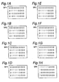
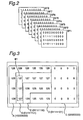
- the PDP subfield method is explained using Fig.'s 1, 2, 3.
- the portion indicated by A in Fig. 3 has a brightness signal level of 128. If this is represented in binary, a (1000 0000) signal level is added to each pixel in the portion indicated by A.
- the portion indicated by B has a brightness of 127, and a (0111 1111) signal level is added to each pixel.
- the portion indicated by C has a brightness of 126, and a (0111 1110) signal level is added to each pixel.
- the portion indicated by D has a brightness of 125, and a (0111 1101) signal level is added to each pixel.
- the portion indicated by E has a brightness of 0, and a (0000 0000) signal level is added to each pixel.
- subfield SF8 is formed by collecting and lining up the most significant bits.
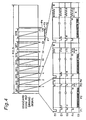
- Fig. 4 shows the standard form of 1 field of a PDP driving signal.
- the processing of each subfield is explained using Fig. 4.
- the processing of each subfield is comprised of setup period P1, write period P2, sustain period P3, and erase period P4.
- setup period P1 a single pulse is applied to a holding electrode E0, and a single pulse is also applied to each scanning electrode E1, E2, E4 (There are only up to 4 scanning electrodes indicated in Fig. 4 because there are only 4 scanning lines shown in the example in Fig. 3, but in reality, there are a plurality of scanning electrodes, 480, for example.).
- preliminary discharge is performed.
- a horizontal-direction scanning electrode scans sequentially, and a prescribed write is performed only to a pixel that received a pulse from a data electrode E5. For example, when processing subfield SF1, a write is performed for a pixel represented by "1" in subfield SF1 depicted in Fig. 2, and a write is not performed for a pixel represented by "0.”
- a sustaining electrode (drive pulse) is outputted in accordance with the weighted value of each subfield.
- a plasma discharge is performed for each sustaining electrode, and the brightness of a predetermined pixel is achieved with one plasma discharge.
- a brightness level of "1” is achieved.
- a brightness level of "2” is achieved. That is, write period P2 is the time when a pixel which is to emit light is selected, and sustain period P3 is the time when light is emitted a number of times that accords with the weighting quantity.
- subfields SF1, SF2, SF3, SF4, SF5, SF6, SF7, SF8 are weighted at 1, 2, 4, 8, 16, 32, 64, 128, respectively. Therefore, the brightness level of each pixel can be adjusted using 256 gradations, from 0 to 255.
- Fig. 5 shows a 2-times mode PDP driving signal.
- the PDP driving signal shown in Fig. 4 is a 1-times mode.
- the number of sustaining pulses comprising sustain period P3 in subfields SF1 through SF8, that is, the weighting values were 1, 2, 4, 8, 16, 32, 64, 128, respectively, but for the 2-times mode of Fig. 5, the number of sustaining pulses comprising sustain period P3 in subfields SF1 through SF8 become 2, 4, 8, 16, 32, 64, 128, 256, respectively, with all subfields being doubled.
- a 2-times mode PDP driving signal can display an image with 2 times the brightness.
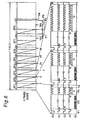
- Fig. 6 shows a 3-times mode PDP driving signal. Therefore, the number of sustaining pulses comprising sustain period P3 in subfields SF1 through SF8 becomes 3, 6, 12, 24, 48, 96, 192, 384, respectively, with all subfields being tripled.
- a mode multiplier is generally expressed as N times. Furthermore, this N can also be expressed as a weighting multiplier N.
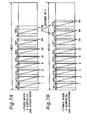
- Fig. 7 (A) shows a standard form PDP driving signal
- Fig. 7 (B) shows a variation of a PDP driving signal, which, by adding 1 subfield comprises subfields SF1 through SF9.
- the final subfield SF8 is weighted by a sustaining pulse of 128, and for the variation in Fig. 7 (B), each of the last 2 subfields SF8, SF9 is weighted by a sustaining pulse of 64.
- a brightness level of 130 is represented, with the standard form of Fig. 7 (A), this can be achieved using both subfield SF2 (weighted 2) and subfield SF8 (weighted 128), whereas with the variation of Fig.
- this brightness level can be achieved using 3 subfields, subfield SF2 (weighted 2), subfield SF8 (weighted 64), and subfield SF9 (weighted 64).
- subfield SF2 weighted 2
- subfield SF8 weighted 64
- subfield SF9 weighted 64
- the number of subfields is generally expressed as Z.
- the subfield number Z is 8, and 1 pixel is represented by 8 bits.
- the subfield number Z is 9, and 1 pixel is represented by 9 bits. That is, in the case of the subfield number Z, 1 pixel is represented by Z bits.
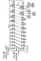
- Fig. 8 shows the development of a PDP driving signal in the past.
- a PDP driving signal changed from a certain field to the next field, if the subfield number Z changed, or the mode number N changed, the light emission center point of the subfield with the largest number of light emissions in each field (hereinafter referred to as the most-weighted subfield) moved.
- the light emission center point refers to the center point between the point in time of light emission start, which is the leading edge of sustain period for a certain subfield, and the point in time of light emission end, which is the trailing edge of sustain period for a certain subfield.
- Fig. 8A shows a field, in which the subfield number Z is 12, and the light emission center point of the most-weighted subfield SF12 is C1.
- Fig. 8B shows a field, in which the subfield number Z is 11, and the light emission center point of the most-weighted subfield SF11 is C2.
- light emission is performed sequentially from the subfield with the smallest number of light emissions to the subfield with the largest number of light emissions.
- the most-weighted subfield undertakes the largest number of light emissions for the field in which this subfield exists, it greatly effects the brightness of that field.
- the length of 1 field for example, is 16.666msec. If the light emission center points of the most-weighted subfields appear at the same cycle (for example, 16.666msec) for a plurality of fields, this can be seen as a natural brightness change, but if the light emission center points of the most-weighted subfields appear as either contiguous or separate, a person viewing the screen will sense an unnatural brightness fluctuation.
- JP-A-06259034 discloses an image display panel in which the subfield weighting is reduced as the subfield number Z is increased in order to fit the increased number of subfields within one field period.
- WO-A-9527970 discloses a display device in which the center of illumination of the various subfields within a field is kept at approximately the same position in time in consecutive fields, each having the same number Z of subfields, by rearranging the order of the subfields within each field and/or by splitting subfields.
- the present invention proposes a PDP display drive pulse controller for preventing light emission center fluctuation, by which the light emission center point of a most-weighted subfield does not fluctuate even when a subfield number Z changes, and/or a mode number N, that is, a weighting multiplier N changes.
- the invention consists in a display drive pulse controller in accordance with that claimed in claim 1.
- the light emission time data which is held in said time data source, is the light emission end point of a most-weighted subfield for different Z values.
- the light emission time data which is held in said time data source, is the light emission start point and the light emission end point of a most-weighted subfield for different Z values.
- said means for calculating said delay time calculates the time difference between the light emission end point of a most-weighted subfield and the end point of the most weighted subfield in a field and the end points of the most-weighted subfields within consecutive fields having different determined subfield numbers Z are located substantially at the same time within their respective fields.
- said means for calculating said delay time calculates the time difference between the light emission center point, which is in the center between the light emission start point and light emission end point, and a predetermined point within a field and the center points of the most-weighted subfields within consecutive fields having different determined subfield numbers Z are located substantially at the same time within their respective fields.
- the invention consists in a display device in accordance with that claimed in claim 6.
- Fig. 9 shows a first embodiment of a PDP display drive pulse controller for preventing light emission center fluctuation, related to the present invention.
- a parameter setting device 1 sets a subfield 'number Z and weighting multiplier N on the basis of brightness and various other data.
- An AID (Analog-to-Digital) converter 2 converts an inputted picture signal to an 8-bit digital signal.
- a picture signal-subfield corresponding device 4 receives a subfield number Z and a weighting multiplier N, and changes the 8-bit signal sent from the A/D converter 2 to a Z-bit signal.
- a subfield unit pulse number setting device 6 receives a subfield number Z and a weighting multiplier N, and specifies the weighting, that is, the number of sustaining pulses required for each subfield.
- a subfield processor 8 outputs a sustaining pulse for sustain period P3 in accordance with data from the subfield unit pulse number setting device 6 for a "1" bit of Z bits.
- setup period P1 for example, 140 ⁇ s
- write period P2 for example, 340 ⁇ s
- an erase period P4 for example, 40 ⁇ s
- 1 cycle of a sustaining pulse is 5 ⁇ s, for example.
- a PDP driving signal created in this way is delayed by a delay circuit 10, and a picture is displayed on a plasma display panel 18.
- Table 1 lists the light emission start point Ls and light emission end point Le of a 1-times mode most-weighted subfield when the subfield number Z is 8, 9, 10, 11, 12, 13, 14, respectively.
- the unit of the numerals in the table is milliseconds. The same holds true for the other tables.
- a light emission start point Ls is expressed as the temporal duration from the leading edge of a field to the light emission start point, and is calculated by using the following formula (1).
- Ls (P1+P2) x SFM + ⁇ f(SFM-1) x P3 + P4 x (SFM-1)
- P1 is setup period (for example, 140 ⁇ s)
- P2 is write period (for example, 340 ⁇ s)
- P3 is 1 cycle time of a sustaining pulse (for example, 5 ⁇ s)
- P4 is erase period (for example, 40 ⁇ s)
- SFM is the subfield number of the most-weighted subfield
- ⁇ f(SFM-1) is the total number of sustaining pulses from subfield SF1 to the subfield immediately prior to the most-weighted subfield. Since the most-weighted subfield appears last in each field, SFM is equivalent to the subfield number in a table.
- the light emission end point Le is expressed as the temporal duration from the leading edge of a field to the light emission end point, and is calculated by using the following formula (2).
- Le Ls + f(SFM) x P3
- f(SFM) is the total number of sustaining pulses in the most-weighted subfield.
- Table 2 Table 3, Table 4, Table 5, Table 6 list the light emission start point Ls and light emission end point Le for each of a 2-times, 3-times, 4-times, 5-times, 6-times mode most-weighted subfield when the subfield number Z is 8, 9, 10, 11, 12, 13, 14, respectively.
- a table selector 14 receives a subfield number Z and weighting multiplier N, and, in addition to selecting a table that accords with the multiplier N, obtains from the selected table the light emission end point Le of a most-weighted subfield that accords with the subfield number Z. Furthermore, since data on the light emission start point Ls of a most-weighted subfield is not required in the embodiment shown in Fig. 9, Fig. 10, the light emission start point row in each table can be omitted, and the data quantity of the table can be reduced.
- a computing unit 16 performs the operation of the following formula (3), calculating delay time Dx.
- Dx Ft - (Le + P4)
- Ft is 1 field time (for example, 16.666ms).
- This delay time Dx is equivalent to the time length of the blank space portion shown at the right end of the PDP driving signal shown in Fig. 8.
- the calculated delay time Dx is sent to a delay device 10, arid a PDP driving signal sent from the subfield processor 8 is delayed by the delay time Dx.
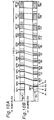
- Fig. 10 shows a PDP driving signal outputted from the delay device 10.
- a signal outputted from the delay device 10 constitutes a signal that is delayed by the delay time Dx of the PDP driving signal of Fig. 8, that is, a signal, for which the light emission end point Le of the most-weighted subfield corresponds to the end point of each field time.
- This is achieved by making use of the fact that, in addition to subfields being arranged in order in each field from the subfield with the least number of light emissions to the subfield with the most, the most-weighted subfield appears last, and by moving to the left end of the PDP driving signal the time length of the blank space portion shown at the right end of the PDP driving signal prior to delay.
- Fig. 11 shows a second embodiment of a PDP display drive pulse controller for preventing light emission center fluctuation, related to the present invention.
- the parameter setting device 1, AID converter 2, picture signal-subfield corresponding device 4, subfield unit pulse number setting device 6, and subfield processor 8 are the same as the first embodiment shown in Fig. 9.
- the subfield time data table 12 also holds the above-described Table 1, Table 2, Table 3, Table 4, Table 5 similar to the above-described first embodiment.
- the table selector 14 receives a subfield number Z and a weighting multiplier N, and, in addition to selecting a table that accords with the multiplier N, obtains from the selected table the light emission start point Ls and light emission end point Le of a most-weighted subfield that accords with the subfield number Z.
- a center point calculating unit 20 finds the light emission center point C of the light emission start point Ls and light emission end point Le using the following formula (4).
- C (Ls + Le)/2
- a center point location setting device 22 sets the location Kc, where the light emission center point of the most-weighted subfield should be, for all possible fields.
- Cmax is the light emission center point C when the light emission end point Le of the most-weighted subfield takes the largest value (in the above-described example, this would be 14.530 for subfield number 14 of Table 6). Further, ⁇ becomes the value that satisfies the following formula (6). Cmax + Max ⁇ f(SFM) x P3 ⁇ /2 + P4 + ⁇ Ft
- Max ⁇ f(SFM) x P3 ⁇ represents the maximum light emission length.
- the maximum light emission length in the above-described example is 3.840ms when the subfield number in Table 6 is 8.
- a subtracting unit 24 subtracts the light emission center point C calculated from location Kc, and calculates a delay time Dx' using the following formula (7).
- Dx' Kc - C
- the subtraction result Dx' is inputted to the delay device 10, and the PDP driving signal is outputted by delaying it by the subtraction result Dx'.
- Fig. 12 shows a PDP driving signal outputted from the delay device 10 of Fig. 11.
- the light emission center point C of the most-weighted subfield can be matched up with location Kc for all fields. In accordance with this, it becomes possible to prevent an unnatural fluctuation in brightness.
- location Kc is accommodated inside a field no matter what most-weighted subfield appears at the end of the field.
Landscapes
- Engineering & Computer Science (AREA)
- Physics & Mathematics (AREA)
- Computer Hardware Design (AREA)
- General Physics & Mathematics (AREA)
- Theoretical Computer Science (AREA)
- Plasma & Fusion (AREA)
- Power Engineering (AREA)
- Control Of Indicators Other Than Cathode Ray Tubes (AREA)
- Control Of Gas Discharge Display Tubes (AREA)
Claims (6)
- Anzeigeimpulssteuervorrichtung für eine Anzeigeeinrichtung (18), wobei die Steuervorrichtung ein Steuersignal in Erwiderung auf ein Bildeingabesignal erzeugt, um die Anzeigeeinrichtung zu veranlassen, Bilder in einer solchen Weise anzuzeigen, dass eine Abstufungsanzeige erzeugt wird, wobei jedes Feld eines Bildeingabesignals durch die Steuervorrichtung in mehrere gewichtete Subfelder unterteilt wird, wobei jedes Feld Daten für Pixel der Anzeigeeinrichtung enthält und eine konstante Dauer unabhängig von der Zahl der gewichteten Subfelder besitzt, wobei die Impulssteuervorrichtung enthält:gekennzeichnet durch eine Zeitdatenquelle (12) zum Halten der Lichtemissionszeitdaten für unterschiedliche Z-Werte, wobei die Lichtemissions-Zeitdaten für jeden Wert von Z die Zeit kennzeichnen, in der das am stärksten gewichtete Subfeld, welches die größte Zahl an Halteimpulsen aller Z Subfelder eines Feldes aufweist, innerhalb jeden Feldes angeordnet ist,Mittel (1) zum Bestimmen der Anzahl Z der Subfelder für jedes Feld des Bildeingabesignals,eine Bildsignal-Subfeldentsprechungseinrichtung (4) zum Ändern des Bildeingabesignals in ein Z-Bit-Helligkeitssignal,eine Subfeldeinheit-Impulszahl-Einstelleinrichtung (6) zum Spezifizieren einer Zahl an Halteimpulsen für jedes der Z Subfelder innerhalb eines Feldes undeinen Subfeldprozessor (8) zum Erzeugen des Steuersignals für jedes Feld basierend auf jedem Subfeld des Z-Bit-Helligkeitssignals und der entsprechenden Zahl an Halteimpulsen,Mittel (14) zum Auswählen der Lichtemissions-Zeitdaten des am stärksten gewichteten Subfeldes eines Feldes, basierend auf der festgelegten Anzahl Z an Subfelder,Mittel (16, 20, 22, 24) zum Berechnen einer Verzögerungszeit (Dx) zum Positionieren des am stärksten gewichteten Subfeldes zu einem vorbestimmten Zeitpunkt in dem Feld basierend auf den gewählten Lichtemissions-Zeitdaten in der Weise, dass innerhalb aufeinander folgender Felder, die eine unterschiedliche Anzahl Z an vorbestimmten Subfeldern aufweisen, das am stärksten gewichtete Subfeld im Wesentlichen zum gleichen relativen Zeitpunkt innerhalb der aufeinander folgenden Felder angeordnet ist, undVerzögerungsmittel (10) zum Verzögern der Ausgabe des Steuersignals an die Anzeigeeinrichtung in Übereinstimmung mit der kalkulierten Verzögerungszeit (Dx).
- Anzeigeimpuls-Steuervorrichtung nach Anspruch 1, bei der die Lichtemissions-Zeitdaten, die in der Zeitdatenquelle gehalten werden, der Lichtemissions-Endpunkt (Le) des am stärksten gewichteten Subfelds für unterschiedliche Z-Werte sind.
- Anzeigeimpuls-Steuervorrichtung nach Anspruch 1, bei der die Lichtemissions-Zeitdaten, die in der Zeitdatenquelle gehalten werden, der Lichtemissions-Startpunkt (Ls) und der Lichtemissions-Endpunkt (Le) des am stärksten gewichteten Subfelds für unterschiedliche Z-Werte ist.
- Anzeigeimpuls-Steuervorrichtung nach Anspruch 2, bei der die Mittel (16) zum Berechnen der Verzögerungszeit (Dx) die Zeitdifferenz zwischen dem Lichtemissions-Endpunkt (Le) des am stärksten gewichteten Subfeldes und dem Endpunkt des am stärksten gewichteten Subfeldes in einem Feld berechnet, wobei die Endpunkte der am stärksten gewichteten Subfelder innerhalb aufeinander folgender Felder mit einer unterschiedlichen vorbestimmten Anzahl Z an Subfeldern im Wesentlichen in der gleichen Zeit innerhalb ihrer entsprechenden Felder angeordnet sind.
- Anzeigeimpuls-Steuervorrichtung nach Anspruch 3, bei der die Mittel (20, 22, 24) zum Berechnen der Verzögerungszeit (Dx) den Zeitunterschied zwischen dem Lichtemissionsmittenpunkt (C), der in der Mitte zwischen dem Lichtemissionsstartpunkt (Ls) und dem Lichtemissionsendpunkt (Le) liegt, und einem vorbestimmten Punkt (Kc) innerhalb eines Feldes berechnet, der sich dort befindet, wo der Lichtemissions-Mittenpunkt des am stärksten gewichteten Subfelds für alle möglichen Werte von Z sein sollte, so dass die Mittenpunkte (C) der am stärksten gewichteten Subfelder innerhalb aufeinander folgender Felder mit einer unterschiedlich Anzahl Z an vorbestimmten Subfeldern im Wesentlichen in der gleichen Relativzeit innerhalb ihrer entsprechenden Felder, basierend auf dem berechneten Unterschied, anordenbar sind.
- Anzeigevorrichtung (18) mit mehreren Pixeln, wobei die Anzeigevorrichtung ein Bildeingangssignal empfängt, welches anschließend in eine Vielzahl von gewichteten Subfeldern unterteilt wird, von denen jedes aufeinander folgend durch die Pixel dargestellt wird, um ein gestuftes Bild zu erzeugen, wobei die Anzeigevorrichtung eine Anzeigeimpuls-Steuervorrichtung gemäß einem der vorstehenden Ansprüche zum Erzeugen eines Steuersignals enthält, welches die Helligkeit jedes Pixels der Anzeigevorrichtung steuert, so dass das am stärksten gewichtete Subfeld für jedes Feld im Wesentlichen zur gleichen Relativzeit innerhalb aufeinander folgender Felder angeordnet ist, wobei die Felder in eine unterschiedliche Anzahl an Subfeldern aufgeteilt worden sind.
Applications Claiming Priority (3)
| Application Number | Priority Date | Filing Date | Title |
|---|---|---|---|
| JP10271999A JP2994632B1 (ja) | 1998-09-25 | 1998-09-25 | 発光中心変動防止のためのpdp表示の駆動パルス制御装置 |
| JP27199998 | 1998-09-25 | ||
| PCT/JP1998/005509 WO2000019400A1 (en) | 1998-09-25 | 1998-12-07 | Plasma display panel drive pulse controller for preventing fluctuation in subframe location |
Publications (2)
| Publication Number | Publication Date |
|---|---|
| EP1032931A1 EP1032931A1 (de) | 2000-09-06 |
| EP1032931B1 true EP1032931B1 (de) | 2002-08-07 |
Family
ID=17507746
Family Applications (1)
| Application Number | Title | Priority Date | Filing Date |
|---|---|---|---|
| EP98957193A Expired - Lifetime EP1032931B1 (de) | 1998-09-25 | 1998-12-07 | Impulssteuervorrichtung für plasmaanzeigetafel zur verhinderung von verschiebungen der unterrahmensposition |
Country Status (8)
| Country | Link |
|---|---|
| US (2) | US6317104B1 (de) |
| EP (1) | EP1032931B1 (de) |
| JP (1) | JP2994632B1 (de) |
| KR (1) | KR100465255B1 (de) |
| CN (1) | CN1128432C (de) |
| DE (1) | DE69807109T2 (de) |
| TW (1) | TW407253B (de) |
| WO (1) | WO2000019400A1 (de) |
Families Citing this family (33)
| Publication number | Priority date | Publication date | Assignee | Title |
|---|---|---|---|---|
| EP1026655A1 (de) * | 1999-02-01 | 2000-08-09 | Deutsche Thomson-Brandt Gmbh | Verfahren zur Leistungspegelsteuerung einer Anzeigeanordnung und Vorrichtung zur Durchführung des Verfahrens |
| WO2002011111A2 (en) * | 2000-07-28 | 2002-02-07 | Thomson Licensing S.A. | Method and apparatus for power level control of a display device |
| JP3876600B2 (ja) * | 2000-09-08 | 2007-01-31 | セイコーエプソン株式会社 | 電気光学装置の駆動方法、電気光学装置の駆動回路、電気光学装置および電子機器 |
| KR100363169B1 (ko) * | 2000-11-17 | 2002-12-05 | 삼성전자 주식회사 | 영상 처리 시스템에 있어서 의사윤곽 보상장치 및 방법 |
| EP1256924B1 (de) * | 2001-05-08 | 2013-09-25 | Deutsche Thomson-Brandt Gmbh | Verfahren und Vorrichtung zur Bearbeitung von Videobildern |
| KR100849002B1 (ko) | 2001-06-12 | 2008-07-30 | 마츠시타 덴끼 산교 가부시키가이샤 | 플라즈마 디스플레이 패널 표시장치 및 그 구동방법 |
| KR100420023B1 (ko) * | 2001-09-25 | 2004-02-25 | 삼성에스디아이 주식회사 | 플라즈마 디스플레이 패널의 계조 표시 장치 및 그 방법 |
| KR100472359B1 (ko) * | 2001-11-28 | 2005-02-21 | 엘지전자 주식회사 | 평균 휘도 레벨 설정방법 |
| EP1331624A1 (de) * | 2002-01-23 | 2003-07-30 | Koninklijke Philips Electronics N.V. | Methode und Vorrichtung zur Ansteuerung eines Plasmabildschirms |
| CN101118722B (zh) * | 2002-03-12 | 2010-10-06 | 日立等离子显示器股份有限公司 | 等离子体显示装置 |
| JP4308488B2 (ja) * | 2002-03-12 | 2009-08-05 | 日立プラズマディスプレイ株式会社 | プラズマディスプレイ装置 |
| JP4064268B2 (ja) * | 2002-04-10 | 2008-03-19 | パイオニア株式会社 | サブフィールド法を用いた表示装置及び表示方法 |
| KR100503603B1 (ko) * | 2003-03-11 | 2005-07-26 | 엘지전자 주식회사 | 플라즈마 디스플레이 패널의 구동방법 |
| EP1667095B1 (de) * | 2003-08-07 | 2009-10-14 | Panasonic Corporation | Display device |
| KR100521471B1 (ko) * | 2004-05-28 | 2005-10-13 | 삼성에스디아이 주식회사 | 서브필드 위치 변동 방지를 위한 플라즈마 디스플레이패널의 구동 방법 및 그 장치 |
| JPWO2005119637A1 (ja) * | 2004-06-02 | 2008-04-03 | 松下電器産業株式会社 | プラズマディスプレイパネル駆動装置及びプラズマディスプレイ |
| US7710361B2 (en) * | 2005-10-18 | 2010-05-04 | Lg Electronics Inc. | Plasma display apparatus and method of driving the same |
| JP5046355B2 (ja) * | 2005-12-26 | 2012-10-10 | 東北パイオニア株式会社 | 映像信号の表示制御装置および表示制御方法 |
| US8111271B2 (en) * | 2006-04-27 | 2012-02-07 | Jasper Display Corporation | Gray scale drive sequences for pulse width modulated displays |
| JP2008096802A (ja) * | 2006-10-13 | 2008-04-24 | Matsushita Electric Ind Co Ltd | プラズマディスプレイパネルの駆動方法およびプラズマディスプレイ装置 |
| US20100103161A1 (en) * | 2006-12-05 | 2010-04-29 | Panasonic Corporation | Plasma display device and method of driving the same |
| US11030942B2 (en) | 2017-10-13 | 2021-06-08 | Jasper Display Corporation | Backplane adaptable to drive emissive pixel arrays of differing pitches |
| TW201928934A (zh) * | 2017-12-26 | 2019-07-16 | 瑞鼎科技股份有限公司 | 應用於有機發光二極體面板之顯示驅動電路及亮度控制方法 |
| US10951875B2 (en) | 2018-07-03 | 2021-03-16 | Raxium, Inc. | Display processing circuitry |
| US11710445B2 (en) | 2019-01-24 | 2023-07-25 | Google Llc | Backplane configurations and operations |
| US11637219B2 (en) | 2019-04-12 | 2023-04-25 | Google Llc | Monolithic integration of different light emitting structures on a same substrate |
| US11238782B2 (en) | 2019-06-28 | 2022-02-01 | Jasper Display Corp. | Backplane for an array of emissive elements |
| US11626062B2 (en) | 2020-02-18 | 2023-04-11 | Google Llc | System and method for modulating an array of emissive elements |
| US12107072B2 (en) | 2020-04-06 | 2024-10-01 | Google Llc | Display backplane including an array of tiles |
| US11538431B2 (en) | 2020-06-29 | 2022-12-27 | Google Llc | Larger backplane suitable for high speed applications |
| US12573349B2 (en) | 2020-06-29 | 2026-03-10 | Google Llc | Efficient image data delivery for an array of pixel memory cells |
| KR102890923B1 (ko) | 2020-12-21 | 2025-11-26 | 구글 엘엘씨 | 자동시청 3d 디스플레이용 고밀도 픽셀 어레이 |
| EP4371104A4 (de) | 2021-07-14 | 2025-06-11 | Google LLC | Rückwandplatine und verfahren zur pulsweitenmodulation |
Family Cites Families (9)
| Publication number | Priority date | Publication date | Assignee | Title |
|---|---|---|---|---|
| JPS6198389A (ja) | 1984-10-20 | 1986-05-16 | 富士通株式会社 | プラズマデイスプレイパネルの輝度補償方法および回路 |
| JP2720607B2 (ja) * | 1990-03-02 | 1998-03-04 | 株式会社日立製作所 | 表示装置、階調表示方法及び駆動回路 |
| JP2795124B2 (ja) * | 1993-03-03 | 1998-09-10 | 株式会社富士通ゼネラル | ディスプレイパネルの中間調画像表示方法 |
| JP3844013B2 (ja) | 1994-04-12 | 2006-11-08 | テキサス インスツルメンツ インコーポレイテツド | ディスプレイ装置 |
| US6025818A (en) * | 1994-12-27 | 2000-02-15 | Pioneer Electronic Corporation | Method for correcting pixel data in a self-luminous display panel driving system |
| JP3891499B2 (ja) | 1995-04-14 | 2007-03-14 | パイオニア株式会社 | プラズマディスプレイパネルにおける輝度調整装置 |
| JP3375473B2 (ja) | 1995-10-31 | 2003-02-10 | 富士通株式会社 | 表示装置及びその駆動方法 |
| JPH10207426A (ja) | 1997-01-21 | 1998-08-07 | Victor Co Of Japan Ltd | プラズマディスプレイパネル表示装置の駆動方法及び駆動制御装置 |
| JPH10222121A (ja) * | 1997-02-03 | 1998-08-21 | Mitsubishi Electric Corp | 画像表示装置及び画像表示方法 |
-
1998
- 1998-09-25 JP JP10271999A patent/JP2994632B1/ja not_active Expired - Fee Related
- 1998-12-07 DE DE69807109T patent/DE69807109T2/de not_active Expired - Lifetime
- 1998-12-07 KR KR10-1999-7006772A patent/KR100465255B1/ko not_active Expired - Fee Related
- 1998-12-07 US US09/355,331 patent/US6317104B1/en not_active Expired - Lifetime
- 1998-12-07 EP EP98957193A patent/EP1032931B1/de not_active Expired - Lifetime
- 1998-12-07 CN CN98802401A patent/CN1128432C/zh not_active Expired - Fee Related
- 1998-12-07 WO PCT/JP1998/005509 patent/WO2000019400A1/en not_active Ceased
- 1998-12-09 TW TW087120467A patent/TW407253B/zh not_active IP Right Cessation
-
2001
- 2001-07-27 US US09/915,505 patent/US6462721B2/en not_active Expired - Fee Related
Also Published As
| Publication number | Publication date |
|---|---|
| WO2000019400A1 (en) | 2000-04-06 |
| DE69807109D1 (de) | 2002-09-12 |
| JP2000098958A (ja) | 2000-04-07 |
| US20010054995A1 (en) | 2001-12-27 |
| US6462721B2 (en) | 2002-10-08 |
| DE69807109T2 (de) | 2003-05-08 |
| CN1266524A (zh) | 2000-09-13 |
| EP1032931A1 (de) | 2000-09-06 |
| CN1128432C (zh) | 2003-11-19 |
| KR100465255B1 (ko) | 2005-01-13 |
| KR20000070527A (ko) | 2000-11-25 |
| TW407253B (en) | 2000-10-01 |
| JP2994632B1 (ja) | 1999-12-27 |
| US6317104B1 (en) | 2001-11-13 |
Similar Documents
| Publication | Publication Date | Title |
|---|---|---|
| US6462721B2 (en) | PDP display drive pulse controller for preventing light emission center fluctuation | |
| KR100359980B1 (ko) | 플라즈마 패널 디스플레이 장치 | |
| JP2994630B2 (ja) | 明るさによるサブフィールド数調整可能な表示装置 | |
| US6476875B2 (en) | Method and apparatus for processing video pictures, especially for false contour effect compensation | |
| JP3425083B2 (ja) | 画像表示装置及び画像評価装置 | |
| AU738827B2 (en) | Dynamic image correction method and dynamic image correction circuit for display Device | |
| KR20090011036A (ko) | 비디오 화상 처리를 위한 방법 및 장치 | |
| KR100603390B1 (ko) | 디스플레이 장치에서의 디스플레이를 위한 비디오 화상을처리하기 위한 방법 및 상기 방법을 수행하기 위한 장치 | |
| KR100286823B1 (ko) | 플라즈마 디스플레이 패널 구동 방법 | |
| JPH09258688A (ja) | ディスプレイ装置 | |
| JP2005165312A (ja) | プラズマディスプレイパネルの駆動装置,プラズマディスプレイパネルの画像処理方法,及びプラズマディスプレイパネル | |
| JP3246217B2 (ja) | ディスプレイパネルの中間調画像表示方法 | |
| JPH0854852A (ja) | ディスプレイパネルの中間調画像表示方法 | |
| EP1732055B1 (de) | Anzeigevorrichtung | |
| JP3493864B2 (ja) | 表示装置の駆動方法及び駆動回路 | |
| JPH08278767A (ja) | ディスプレイ装置の駆動方法 | |
| KR100425486B1 (ko) | 플라즈마 디스플레이 패널의 영상신호 처리 장치 | |
| JPH10161586A (ja) | 表示装置の駆動方法及び駆動回路 | |
| KR100432667B1 (ko) | 플라즈마 디스플레이 패널의 계조 표시 방법 및 그 장치 | |
| JP2003255886A (ja) | 表示装置及び階調表示方法 | |
| JPH1039833A (ja) | ディスプレイ装置の階調歪み補正回路 | |
| EP0987675A1 (de) | Vorrichtung und Verfahren zur Video-Bildbearbeitung, insbesondere zur Kompensation des Falschkontureneffekts |
Legal Events
| Date | Code | Title | Description |
|---|---|---|---|
| PUAI | Public reference made under article 153(3) epc to a published international application that has entered the european phase |
Free format text: ORIGINAL CODE: 0009012 |
|
| 17P | Request for examination filed |
Effective date: 20000526 |
|
| AK | Designated contracting states |
Kind code of ref document: A1 Designated state(s): DE FR GB |
|
| 17Q | First examination report despatched |
Effective date: 20001120 |
|
| GRAG | Despatch of communication of intention to grant |
Free format text: ORIGINAL CODE: EPIDOS AGRA |
|
| GRAG | Despatch of communication of intention to grant |
Free format text: ORIGINAL CODE: EPIDOS AGRA |
|
| GRAG | Despatch of communication of intention to grant |
Free format text: ORIGINAL CODE: EPIDOS AGRA |
|
| GRAH | Despatch of communication of intention to grant a patent |
Free format text: ORIGINAL CODE: EPIDOS IGRA |
|
| GRAH | Despatch of communication of intention to grant a patent |
Free format text: ORIGINAL CODE: EPIDOS IGRA |
|
| GRAA | (expected) grant |
Free format text: ORIGINAL CODE: 0009210 |
|
| AK | Designated contracting states |
Kind code of ref document: B1 Designated state(s): DE FR GB |
|
| REG | Reference to a national code |
Ref country code: GB Ref legal event code: FG4D |
|
| REF | Corresponds to: |
Ref document number: 69807109 Country of ref document: DE Date of ref document: 20020912 |
|
| ET | Fr: translation filed | ||
| PLBE | No opposition filed within time limit |
Free format text: ORIGINAL CODE: 0009261 |
|
| STAA | Information on the status of an ep patent application or granted ep patent |
Free format text: STATUS: NO OPPOSITION FILED WITHIN TIME LIMIT |
|
| 26N | No opposition filed |
Effective date: 20030508 |
|
| REG | Reference to a national code |
Ref country code: GB Ref legal event code: 746 Effective date: 20100127 |
|
| PGFP | Annual fee paid to national office [announced via postgrant information from national office to epo] |
Ref country code: DE Payment date: 20121205 Year of fee payment: 15 |
|
| PGFP | Annual fee paid to national office [announced via postgrant information from national office to epo] |
Ref country code: GB Payment date: 20121205 Year of fee payment: 15 |
|
| PGFP | Annual fee paid to national office [announced via postgrant information from national office to epo] |
Ref country code: FR Payment date: 20130107 Year of fee payment: 15 |
|
| REG | Reference to a national code |
Ref country code: DE Ref legal event code: R119 Ref document number: 69807109 Country of ref document: DE |
|
| GBPC | Gb: european patent ceased through non-payment of renewal fee |
Effective date: 20131207 |
|
| REG | Reference to a national code |
Ref country code: FR Ref legal event code: ST Effective date: 20140829 |
|
| REG | Reference to a national code |
Ref country code: DE Ref legal event code: R119 Ref document number: 69807109 Country of ref document: DE Effective date: 20140701 |
|
| PG25 | Lapsed in a contracting state [announced via postgrant information from national office to epo] |
Ref country code: DE Free format text: LAPSE BECAUSE OF NON-PAYMENT OF DUE FEES Effective date: 20140701 |
|
| PG25 | Lapsed in a contracting state [announced via postgrant information from national office to epo] |
Ref country code: GB Free format text: LAPSE BECAUSE OF NON-PAYMENT OF DUE FEES Effective date: 20131207 Ref country code: FR Free format text: LAPSE BECAUSE OF NON-PAYMENT OF DUE FEES Effective date: 20131231 |