EP1033593A1 - Dispositif de routage ayant un réseau optique formé par un guide d'ondes à spectre d'amplitude composite prédéterminé - Google Patents
Dispositif de routage ayant un réseau optique formé par un guide d'ondes à spectre d'amplitude composite prédéterminé Download PDFInfo
- Publication number
- EP1033593A1 EP1033593A1 EP00301585A EP00301585A EP1033593A1 EP 1033593 A1 EP1033593 A1 EP 1033593A1 EP 00301585 A EP00301585 A EP 00301585A EP 00301585 A EP00301585 A EP 00301585A EP 1033593 A1 EP1033593 A1 EP 1033593A1
- Authority
- EP
- European Patent Office
- Prior art keywords
- output
- input
- waveguides
- loss
- waveguide
- Prior art date
- Legal status (The legal status is an assumption and is not a legal conclusion. Google has not performed a legal analysis and makes no representation as to the accuracy of the status listed.)
- Granted
Links
- 238000001228 spectrum Methods 0.000 claims abstract description 44
- 239000002131 composite material Substances 0.000 claims abstract description 31
- 238000000034 method Methods 0.000 claims abstract description 10
- 230000003287 optical effect Effects 0.000 claims description 27
- 230000005855 radiation Effects 0.000 claims description 7
- 230000001747 exhibiting effect Effects 0.000 claims description 4
- 238000000411 transmission spectrum Methods 0.000 abstract 1
- 230000005540 biological transmission Effects 0.000 description 8
- 238000010586 diagram Methods 0.000 description 2
- 239000002019 doping agent Substances 0.000 description 2
- 239000013307 optical fiber Substances 0.000 description 2
- 230000010363 phase shift Effects 0.000 description 2
- 229910052691 Erbium Inorganic materials 0.000 description 1
- 230000003321 amplification Effects 0.000 description 1
- 238000003491 array Methods 0.000 description 1
- 230000000694 effects Effects 0.000 description 1
- 230000008030 elimination Effects 0.000 description 1
- 238000003379 elimination reaction Methods 0.000 description 1
- 238000005516 engineering process Methods 0.000 description 1
- UYAHIZSMUZPPFV-UHFFFAOYSA-N erbium Chemical compound [Er] UYAHIZSMUZPPFV-UHFFFAOYSA-N 0.000 description 1
- 238000010348 incorporation Methods 0.000 description 1
- 239000011159 matrix material Substances 0.000 description 1
- 238000003199 nucleic acid amplification method Methods 0.000 description 1
- 230000002250 progressing effect Effects 0.000 description 1
- 229910052761 rare earth metal Inorganic materials 0.000 description 1
- 150000002910 rare earth metals Chemical class 0.000 description 1
- 239000004065 semiconductor Substances 0.000 description 1
- 238000007493 shaping process Methods 0.000 description 1
Images


Classifications
-
- G—PHYSICS
- G02—OPTICS
- G02B—OPTICAL ELEMENTS, SYSTEMS OR APPARATUS
- G02B6/00—Light guides; Structural details of arrangements comprising light guides and other optical elements, e.g. couplings
- G02B6/10—Light guides; Structural details of arrangements comprising light guides and other optical elements, e.g. couplings of the optical waveguide type
- G02B6/12—Light guides; Structural details of arrangements comprising light guides and other optical elements, e.g. couplings of the optical waveguide type of the integrated circuit kind
- G02B6/12007—Light guides; Structural details of arrangements comprising light guides and other optical elements, e.g. couplings of the optical waveguide type of the integrated circuit kind forming wavelength selective elements, e.g. multiplexer, demultiplexer
- G02B6/12009—Light guides; Structural details of arrangements comprising light guides and other optical elements, e.g. couplings of the optical waveguide type of the integrated circuit kind forming wavelength selective elements, e.g. multiplexer, demultiplexer comprising arrayed waveguide grating [AWG] devices, i.e. with a phased array of waveguides
- G02B6/12016—Light guides; Structural details of arrangements comprising light guides and other optical elements, e.g. couplings of the optical waveguide type of the integrated circuit kind forming wavelength selective elements, e.g. multiplexer, demultiplexer comprising arrayed waveguide grating [AWG] devices, i.e. with a phased array of waveguides characterised by the input or output waveguides, e.g. tapered waveguide ends, coupled together pairs of output waveguides
-
- G—PHYSICS
- G02—OPTICS
- G02B—OPTICAL ELEMENTS, SYSTEMS OR APPARATUS
- G02B6/00—Light guides; Structural details of arrangements comprising light guides and other optical elements, e.g. couplings
- G02B6/10—Light guides; Structural details of arrangements comprising light guides and other optical elements, e.g. couplings of the optical waveguide type
- G02B6/12—Light guides; Structural details of arrangements comprising light guides and other optical elements, e.g. couplings of the optical waveguide type of the integrated circuit kind
- G02B6/12007—Light guides; Structural details of arrangements comprising light guides and other optical elements, e.g. couplings of the optical waveguide type of the integrated circuit kind forming wavelength selective elements, e.g. multiplexer, demultiplexer
- G02B6/12009—Light guides; Structural details of arrangements comprising light guides and other optical elements, e.g. couplings of the optical waveguide type of the integrated circuit kind forming wavelength selective elements, e.g. multiplexer, demultiplexer comprising arrayed waveguide grating [AWG] devices, i.e. with a phased array of waveguides
- G02B6/12019—Light guides; Structural details of arrangements comprising light guides and other optical elements, e.g. couplings of the optical waveguide type of the integrated circuit kind forming wavelength selective elements, e.g. multiplexer, demultiplexer comprising arrayed waveguide grating [AWG] devices, i.e. with a phased array of waveguides characterised by the optical interconnection to or from the AWG devices, e.g. integration or coupling with lasers or photodiodes
-
- G—PHYSICS
- G02—OPTICS
- G02B—OPTICAL ELEMENTS, SYSTEMS OR APPARATUS
- G02B6/00—Light guides; Structural details of arrangements comprising light guides and other optical elements, e.g. couplings
- G02B6/10—Light guides; Structural details of arrangements comprising light guides and other optical elements, e.g. couplings of the optical waveguide type
- G02B6/12—Light guides; Structural details of arrangements comprising light guides and other optical elements, e.g. couplings of the optical waveguide type of the integrated circuit kind
- G02B6/12007—Light guides; Structural details of arrangements comprising light guides and other optical elements, e.g. couplings of the optical waveguide type of the integrated circuit kind forming wavelength selective elements, e.g. multiplexer, demultiplexer
- G02B6/12009—Light guides; Structural details of arrangements comprising light guides and other optical elements, e.g. couplings of the optical waveguide type of the integrated circuit kind forming wavelength selective elements, e.g. multiplexer, demultiplexer comprising arrayed waveguide grating [AWG] devices, i.e. with a phased array of waveguides
- G02B6/12033—Light guides; Structural details of arrangements comprising light guides and other optical elements, e.g. couplings of the optical waveguide type of the integrated circuit kind forming wavelength selective elements, e.g. multiplexer, demultiplexer comprising arrayed waveguide grating [AWG] devices, i.e. with a phased array of waveguides characterised by means for configuring the device, e.g. moveable element for wavelength tuning
Definitions
- the invention relates generally to optical devices and, more particularly, to waveguide grating routers.
- Waveguide grating routers in conventional lightwave systems are used as optical switches, multiplexers, demultiplexers, detectors, add/drop filters, one by N (1 X N) and N by one (N X 1) splitters and N by N (N X N) arrays.
- Such waveguide grating routers include an interconnection apparatus having a plurality of closely spaced input waveguides communicating with an input of a star coupler.
- An output of the star coupler communicates with an optical grating comprising a series of optical waveguides in which each of the grating waveguides differ in length with respect to its nearest neighbor by a predetermined fixed amount.
- the optical grating is further connected to an input of a second star coupler, the outputs of which form outputs of the switching, multiplexing, and demultiplexing apparatus.
- Waveguide grating routers are also frequently referred to as "frequency routing devices" and are further described in U. S. Patent No. 5,002,350, issued March 26, 1991 to C. Dragone, entitled “Optical Multiplexer/Demultiplexer” (hereinafter "Dragone 1”) and U. S. Patent No. 5, 136,671, issued August 4, 1992 to C. Dragone, entitled “Optical Switch, Multiplexer, and Demultiplexer” (hereinafter "Dragone 2”), both of which are hereby incorporated by reference.
- a known characteristic of these waveguide grating routers is that they do not efficiently provide a predetermined composite amplitude spectrum for each of the output signals that may comprise many wavelengths or frequencies. Rather, these routers tend to attenuate signals in outer waveguides more than signals in the inner waveguides. Thus, the amplitude response of the router across the spectrum of wavelengths in the waveguides is nonuniform.
- a waveguide grating router having a predetermined composite amplitude spectrum is achieved in accordance with the principles of the present invention by introducing loss into the waveguide grating router's waveguides.
- the desired predetermined composite amplitude spectrum is a uniform amplitude spectrum, this same loss can produce loss equalization by the complete elimination of gain nonuniformity in all the output signals.
- the invention however is not limited to the production of a flat amplitude spectrum.
- the predetermined composite amplitude spectrum may be sinusoidal, triangular, stepwise discrete, sloped, logarithmic, etc.
- a waveguide grating router includes at least one input waveguide and a plurality of output waveguides.
- a variable loss element is introduced to a predetermined group of output waveguides to produce a predetermined composite amplitude spectrum of the output signals.
- a waveguide grating router that includes a plurality of input waveguide and a plurality of output waveguides.
- the variable loss element is introduced loss to a predetermined group of both input and output waveguides to yield output signals that exhibit the predetermined composite amplitude spectrum.
- loss may be introduced in a variety of ways, including varying the cross-section of an input waveguide with respect to that of an output waveguide.
- a waveguide grating router is also known as a frequency routing device.
- the latter term describes the action of light at different frequencies taking different paths through the router.
- the terms "frequency” and “wavelength” may be used interchangeably when referring to the operation of the router.
- Optical grating 106 includes a plurality of unequal length waveguides that provide a predetermined amount of path length difference to the corresponding plurality of input waveguides 102 i .
- a signal of amplitude A is applied to one of the input waveguides 102 i , for example, input waveguide 102 1 .
- signals of amplitudes AT 11 , AT 12 , ...AT 1N are produced at output waveguides 110 k where T ik is the value of the transmission coefficient for input waveguide 102 1 and the plurality of output waveguides 110 k .
- output signals from the plurality of output waveguides 110 k of the waveguide grating router form a Gaussian amplitude spectrum.
- the composite amplitude spectrum of the output signals as a function of wavelength is shown illustrating the corresponding transmission coefficients T ik for the routing device.
- the details of the routing devices' constriction and operation are more fully described in Dragone 1, Dragone 2, and U. S. Patent No. 5,243,672, issued September 7, 1993 to C. Dragone, entitled “Planar Waveguide Having Optimized Bend", (hereinafter "Dragone 3"), which is hereby incorporated by reference.
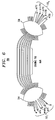
- FIG. 3 illustrates an embodiment of a waveguide grating router 300 in accordance with the present invention.
- Waveguide grating router 300 includes all of the elements of FIG. 1 including a plurality of input waveguides 302, a first free space region 304, an optical grating 306, a second free space region 308, and a plurality of output waveguides 310.
- waveguide grating router 300 also includes a plurality of variable loss elements 320.
- the plurality of variable loss elements 320 are optically coupled to a predetermined set of the output waveguides 310 to produce a predetermined composite amplitude spectrum in the output signals.
- variable loss elements 320 may be optically coupled to a predetermined set of input waveguides 302, instead of output waveguides 310, to produce a predetermined composite amplitude spectrum in the output signals. Variable loss permits shaping of the output signals from each waveguide independent of each other.
- the waveguide grating router of FIG. 3 directs a multiwavelength-input signal through a predetermined one of the input waveguides 302, where the input signal is a multiplexed signal with wavelengths, ⁇ 1 , ⁇ 2 , ... ⁇ n .
- the input signal is demultiplexed into component wavelengths with each of the component wavelengths directed to a predetermined one of the output waveguides 302 of the router.
- the input signal is transmitted through the first free space region 304 to the optical grating 306. Due to differing lengths and curvatures of each waveguide that are separated by a fixed amount within the optical grating 306, the optical grating 306 phase-shifts each signal transmitted through each waveguide.
- the multiwavelength signal is directed through the router and separates into a number of output signals each exhibiting a wavelength component of the original input signal.
- Variable loss elements 320 apply loss to each output signal in a predetermined amount to achieve the desired predetermined composite amplitude spectrum.
- an amplifier 322 may be optically coupled to the plurality of output waveguides 310 to amplify the output signals after the loss is applied. The amplifier 322 will receive and amplify these output signals. Amplification is desirable in cases where a specific power level is required.
- loss elements 320 of FIG 3 can be configured to alter the output signals, producing such a uniform composite amplitude spectrum. For example, if a 1 X N waveguide grating router exhibiting a Gaussian amplitude spectrum, as shown in FIG. 2, is desired, the greatest loss should be introduced at the output waveguides closest to the center and less loss introduced at each adjacent port waveguide progressing toward the outermost waveguides.
- Loss may be introduced in a variety of ways.
- One way is to vary the cross-sectional area of the output waveguides to the cross-sectional area of the input waveguide. This may be implemented, for example, by varying the waveguide widths, heights, cross-sectional shapes, position, and angular tilt.
- offsetting each connection of the output waveguides for example, offset centers or intentional misalignment of the optical fiber which links the routing device to the rest of the multiwavelength lightwave system creates the same effect.
- loss can be introduced by an output waveguide having different cross-sectional areas at different sections of the same output waveguide. For example, in Fig. 5, output waveguide 510 can have a larger cross-sectional area near the free space region 508 and a smaller cross-sectional area at the opposite end.
- loss can be introduced by "siphoning light" into a "dummy" waveguide.
- a dummy waveguide can be placed near the output waveguides so that a portion of the multiwavelength signal couples to the dummy waveguide. This is accomplished with directional coupler or a Y-branch splitter/tap.
- Still another way to introduce loss is through wavelength selective filters, such as asymmetrical Mach Zehnder interferometers or gratings, such as long period, Bragg and/or chirped.
- integrated loss may be made variable by placing an electrode over each output waveguide. Then, by electrically addressing each electrode with an appropriate signal, the loss, via refractive index changes, could be variably tuned.
- the incorporation of a dopant similar to rare earth dopants for optical fibers, such as erbium, may be useful for tuning the loss where the loss elements are semiconductor devices.
- the waveguide grating router 500 shown therein includes a plurality of input waveguides 502, a first free space region 504, an optical grating 506, a second free space region 508, and a plurality of output waveguides 510 - 518.
- the output waveguides 510 - 518 are designed in such a way as to differ in cross-sectional width from that of the input waveguides 502.
- waveguide grating router 500 includes a plurality of output waveguides 510 - 518 having a center waveguide 514 and adjacent waveguides 512 and 516, as illustrated.
- the center waveguide 514 has a width of ⁇
- the adjacent waveguides 512 and 516 have a width of ⁇
- waveguides 510 and 518 have a width of ⁇ , where ⁇ > ⁇ > ⁇ and each coordinate is adjusted in such a way that the router's output signals exhibit a uniform amplitude spectrum.
- the center waveguide 514 has the greatest cross-sectional width.
- waveguides 512 and 516 adjacent to the center waveguides are smaller in cross-section than waveguide 514 and the waveguides 510 and 518 are smaller in cross-section than waveguides 512 and 516.
- These output signals incur loss proportional to the cross-sectional width of each output waveguide, thus, a uniform amplitude spectrum is achieved.
- f i and f k are the radiation fields at the cross-section of the input waveguide i and output waveguide k and x and y are the spatial coordinates that span the cross-section. Accordingly, the better the match or overlap the lower the loss therein.
- the fields between two waveguides are a combination of radiation fields and waveguide modes, whose number, extent, shape, character, etc., depend on the size, shape, and index of the waveguide.
- This overlap integral can also describe relative differences in angular tilt and spatial position.
- loss elements can be introduced to the input waveguides with respect to the loss elements introduced to the output waveguides to produce the desired predetermined composite amplitude spectrum.
- the transmission coefficients T ik of a N X N waveguide grating router form a N X N matrix, there are N 2 independent values that must be accounted for to introduce the desired losses to produce the desired predetermined composite amplitude spectrum.
- the transmission T ik coefficients values are interdependent, they can be modified (or equalized to achieve a uniform composite amplitude spectrum) by using only 2N adjustments to the waveguides.
- the N 2 transmission coefficients can be satisfied because not all of the radiation fields are unique and not all of the transmission coefficients are unique.
- complete equalization of a N X N waveguide grating router with N 2 possible transmission T ik coefficients can be accomplished with 2(N-2) adjustments to the waveguides, as shown in FIG. 6.
- the waveguide grating router includes a plurality of input waveguides 702 i , a first free space region 704, an optical grating 706, a second free space region 708, and a plurality of output waveguides 730 k .
- a plurality of multiwavelength signals is received by the plurality of input waveguides 702.
- the signals are coupled at the first free space region 704.
- the coupled signal is launched into the optical grating 706.
- each waveguide Due to differing lengths and curvature of each waveguide within the optical grating 706, where each waveguide is separated by a fixed amount the optical grating 706 phase-shifts each signal transmitted through each output waveguide.
- the multiwavelength signals received by the plurality of input waveguides are transmitted through the router and separated into output signals, each having a specific wavelength component of the signals received. Since the cross-sectional widths of the plurality of input waveguides 702 i differ from the cross-sectional widths of the plurality of output waveguides 730 k , the signals suffer loss such that a uniform amplitude spectrum is achieved.
- the widths of the input waveguides 702 i are set in such a fashion as to allow the center input waveguide to experience the greatest loss and, correspondingly, each adjacent waveguide thereafter experiences less loss.
- the widths of the plurality of output waveguides 730 k are set such that the center output waveguide experience the least loss and, correspondingly, each adjacent waveguide thereafter experiences greater loss.
Landscapes
- Physics & Mathematics (AREA)
- Engineering & Computer Science (AREA)
- Microelectronics & Electronic Packaging (AREA)
- General Physics & Mathematics (AREA)
- Optics & Photonics (AREA)
- Optical Integrated Circuits (AREA)
Priority Applications (2)
| Application Number | Priority Date | Filing Date | Title |
|---|---|---|---|
| EP10185919A EP2273293A3 (fr) | 1999-03-02 | 2000-02-28 | Dispositif de routage ayant un réseau optique formé par des guides d'ondes optiques à spectre d'amplitude composite prédéterminé |
| EP10163010A EP2221644A1 (fr) | 1999-03-02 | 2000-02-28 | Dispositif de routage ayant un réseau optique formé par des guides d'ondes optiques à spectre d'amplitude composite prédéterminé |
Applications Claiming Priority (2)
| Application Number | Priority Date | Filing Date | Title |
|---|---|---|---|
| US260635 | 1981-05-05 | ||
| US09/260,635 US6205273B1 (en) | 1999-03-02 | 1999-03-02 | Waveguide grating router having a predetermined composite amplitude spectrum |
Related Child Applications (2)
| Application Number | Title | Priority Date | Filing Date |
|---|---|---|---|
| EP10163010.1 Division-Into | 2010-05-17 | ||
| EP10185919.7 Division-Into | 2010-10-01 |
Publications (2)
| Publication Number | Publication Date |
|---|---|
| EP1033593A1 true EP1033593A1 (fr) | 2000-09-06 |
| EP1033593B1 EP1033593B1 (fr) | 2010-12-01 |
Family
ID=22989975
Family Applications (3)
| Application Number | Title | Priority Date | Filing Date |
|---|---|---|---|
| EP10163010A Withdrawn EP2221644A1 (fr) | 1999-03-02 | 2000-02-28 | Dispositif de routage ayant un réseau optique formé par des guides d'ondes optiques à spectre d'amplitude composite prédéterminé |
| EP00301585A Expired - Lifetime EP1033593B1 (fr) | 1999-03-02 | 2000-02-28 | Dispositif de routage ayant un réseau optique formé par des guides d'ondes optiques à spectre d'amplitude composite prédéterminé, procédé correspondant et son usage |
| EP10185919A Withdrawn EP2273293A3 (fr) | 1999-03-02 | 2000-02-28 | Dispositif de routage ayant un réseau optique formé par des guides d'ondes optiques à spectre d'amplitude composite prédéterminé |
Family Applications Before (1)
| Application Number | Title | Priority Date | Filing Date |
|---|---|---|---|
| EP10163010A Withdrawn EP2221644A1 (fr) | 1999-03-02 | 2000-02-28 | Dispositif de routage ayant un réseau optique formé par des guides d'ondes optiques à spectre d'amplitude composite prédéterminé |
Family Applications After (1)
| Application Number | Title | Priority Date | Filing Date |
|---|---|---|---|
| EP10185919A Withdrawn EP2273293A3 (fr) | 1999-03-02 | 2000-02-28 | Dispositif de routage ayant un réseau optique formé par des guides d'ondes optiques à spectre d'amplitude composite prédéterminé |
Country Status (3)
| Country | Link |
|---|---|
| US (1) | US6205273B1 (fr) |
| EP (3) | EP2221644A1 (fr) |
| JP (1) | JP3939894B2 (fr) |
Cited By (4)
| Publication number | Priority date | Publication date | Assignee | Title |
|---|---|---|---|---|
| WO2004015470A1 (fr) * | 2002-08-08 | 2004-02-19 | Agere Systems Inc. | Dispositif optique |
| JP3517877B2 (ja) | 2000-09-05 | 2004-04-12 | 住友電気工業株式会社 | 光合分波器 |
| WO2005052660A1 (fr) * | 2003-11-28 | 2005-06-09 | Nhk Spring Co., Ltd. | Multiplexeur/demultiplexeur du type a reseau de diffraction et guide d'onde en reseau multi-canaux, et procede pour connecter un guide d'onde en reseau avec des guides d'onde de sortie |
| EP1777561A1 (fr) * | 2005-10-24 | 2007-04-25 | NEC Corporation | Dispositif à guide d'onde optique et procédé de réglage d'une perte de transmission de celui-ci |
Families Citing this family (24)
| Publication number | Priority date | Publication date | Assignee | Title |
|---|---|---|---|---|
| DE19815404A1 (de) * | 1998-04-06 | 1999-10-14 | Siemens Ag | Anordnung zur räumlichen Trennung und/oder Zusammenführung optischer Wellenlängenkanäle |
| US6529670B1 (en) | 1999-07-08 | 2003-03-04 | The Furukawa Electric Co., Ltd. | Optical fiber array and optical light-wave device, and connecting the same |
| US6512864B1 (en) * | 2000-06-08 | 2003-01-28 | Lucent Technologies Inc. | Optical multiplexer/demultiplexer arrangement for WDM signals having in-band and out-of-band signal components |
| JP3736303B2 (ja) | 2000-06-29 | 2006-01-18 | 日本電気株式会社 | アレイ導波路格子、マルチプレクサ装置、デマルチプレクサ装置、ノード装置および光通信システム |
| JP3890190B2 (ja) * | 2000-11-16 | 2007-03-07 | 日本電気株式会社 | アレイ導波路格子および導波路素子 |
| CA2328696C (fr) * | 2000-12-18 | 2008-08-12 | Jds Uniphase Inc. | Multiplexeur/demultiplexeur periodique a reseau de guides d'onde |
| US6697552B2 (en) | 2001-02-23 | 2004-02-24 | Lightwave Microsystems Corporation | Dendritic taper for an integrated optical wavelength router |
| GB0106014D0 (en) * | 2001-03-12 | 2001-05-02 | Kymata Ltd | Arrayed waveguide grating |
| US6853769B2 (en) * | 2001-03-16 | 2005-02-08 | Lightwave Microsystems Corporation | Arrayed waveguide grating with waveguides of unequal widths |
| US6850670B2 (en) * | 2001-06-28 | 2005-02-01 | Lightwave Microsytstems Corporation | Method and apparatus for controlling waveguide birefringence by selection of a waveguide core width for a top clad |
| US6900932B2 (en) * | 2001-09-20 | 2005-05-31 | Bayspec, Inc. | Optical gain flattening filter using VPG-based optical elements |
| JP2003172830A (ja) * | 2001-12-04 | 2003-06-20 | Fujitsu Ltd | 光合分波器 |
| AU2003227262A1 (en) * | 2002-03-28 | 2003-10-13 | Hitachi Chemical Co., Ltd. | Optical waveguide and optical multiplexer/demultiplexer |
| US7095923B1 (en) * | 2002-03-29 | 2006-08-22 | Nortel Networks Limited | Wavelength selective optical filter |
| US20040047537A1 (en) * | 2002-09-06 | 2004-03-11 | Boord Warren Timothy | Fan-out circuit with integrated active and passive components |
| US7065273B2 (en) * | 2003-06-20 | 2006-06-20 | Intel Corporation | Wideband arrayed waveguide grating |
| US7266401B2 (en) | 2003-08-22 | 2007-09-04 | C8 Medisensors Inc. | Measuring analytes from an electromagnetic spectrum using a wavelength router |
| JP2005266381A (ja) * | 2004-03-19 | 2005-09-29 | Nec Corp | 導波路型光スプリッタ及びこれを備えた導波路型光モジュール |
| JP4505313B2 (ja) * | 2004-11-12 | 2010-07-21 | 富士通株式会社 | 光装置および光制御方法 |
| JP2005321820A (ja) * | 2005-06-16 | 2005-11-17 | Nec Corp | アレイ導波路格子、アレイ導波路格子モジュール、光通信装置および光通信システム |
| US7609917B2 (en) * | 2005-10-11 | 2009-10-27 | Lightwave Microsystems Corporation | Method and apparatus for controlling waveguide birefringence by selection of a waveguide core width for a top cladding |
| CN106605340B (zh) * | 2015-08-18 | 2020-07-10 | 古河电气工业株式会社 | 光半导体装置 |
| CN105467518B (zh) * | 2015-12-29 | 2019-05-21 | 北京大学 | 一种可调光功分比的星型耦合器及其实现方法 |
| CN115469398A (zh) * | 2022-09-19 | 2022-12-13 | 华东光电集成器件研究所 | 输入端口为不对称锥形结构的阵列波导光栅、通信装置 |
Citations (3)
| Publication number | Priority date | Publication date | Assignee | Title |
|---|---|---|---|---|
| US5243672A (en) * | 1992-08-04 | 1993-09-07 | At&T Bell Laboratories | Planar waveguide having optimized bend |
| US5706377A (en) | 1996-07-17 | 1998-01-06 | Lucent Technologies Inc. | Wavelength routing device having wide and flat passbands |
| EP0881512A2 (fr) * | 1997-05-28 | 1998-12-02 | Lucent Technologies Inc. | Dispositif d'acheminement de signaux avec couplage de modes guidés multiples afin de produire un rayonnement conformé à canux multiples |
Family Cites Families (10)
| Publication number | Priority date | Publication date | Assignee | Title |
|---|---|---|---|---|
| DE3416493A1 (de) * | 1984-05-04 | 1985-11-07 | Standard Elektrik Lorenz Ag, 7000 Stuttgart | Optische empfangseinrichtung |
| GB8429430D0 (en) * | 1984-11-21 | 1985-01-03 | Gen Electric Co Plc | Optical couplers |
| US5002350A (en) | 1990-02-26 | 1991-03-26 | At&T Bell Laboratories | Optical multiplexer/demultiplexer |
| US5136671A (en) | 1991-08-21 | 1992-08-04 | At&T Bell Laboratories | Optical switch, multiplexer, and demultiplexer |
| CA2136752C (fr) * | 1992-06-26 | 2003-04-15 | Minnesota Mining And Manufacturing Company | Commutateur optique numerique multibranchement |
| US5519796A (en) * | 1995-03-06 | 1996-05-21 | International Business Machines Corporation | Gain equalization using monolithic planar waveguide grating multiplexer and demultiplexer |
| US6025947A (en) * | 1996-05-02 | 2000-02-15 | Fujitsu Limited | Controller which controls a variable optical attenuator to control the power level of a wavelength-multiplexed optical signal when the number of channels are varied |
| US5881199A (en) * | 1996-12-02 | 1999-03-09 | Lucent Technologies Inc. | Optical branching device integrated with tunable attenuators for system gain/loss equalization |
| JP2858655B2 (ja) * | 1997-01-22 | 1999-02-17 | 日立電線株式会社 | 光波長合分波器 |
| US5953467A (en) * | 1997-09-23 | 1999-09-14 | Lucent Technologies Inc. | Switchable optical filter |
-
1999
- 1999-03-02 US US09/260,635 patent/US6205273B1/en not_active Expired - Lifetime
-
2000
- 2000-02-28 EP EP10163010A patent/EP2221644A1/fr not_active Withdrawn
- 2000-02-28 EP EP00301585A patent/EP1033593B1/fr not_active Expired - Lifetime
- 2000-02-28 EP EP10185919A patent/EP2273293A3/fr not_active Withdrawn
- 2000-03-01 JP JP2000056109A patent/JP3939894B2/ja not_active Expired - Fee Related
Patent Citations (3)
| Publication number | Priority date | Publication date | Assignee | Title |
|---|---|---|---|---|
| US5243672A (en) * | 1992-08-04 | 1993-09-07 | At&T Bell Laboratories | Planar waveguide having optimized bend |
| US5706377A (en) | 1996-07-17 | 1998-01-06 | Lucent Technologies Inc. | Wavelength routing device having wide and flat passbands |
| EP0881512A2 (fr) * | 1997-05-28 | 1998-12-02 | Lucent Technologies Inc. | Dispositif d'acheminement de signaux avec couplage de modes guidés multiples afin de produire un rayonnement conformé à canux multiples |
Non-Patent Citations (2)
| Title |
|---|
| CHEN J C ET AL: "WAVEGUIDE GRATING ROUTERS WITH GREATER CHANNEL UNIFORMITY", ELECTRONICS LETTERS,GB,IEE STEVENAGE, vol. 33, no. 23, 6 November 1997 (1997-11-06), pages 1951 - 1952, XP000773524, ISSN: 0013-5194 * |
| ISHIDA O ET AL: "LOSS-IMBALANCE EQUALIZATION IN ARRAYED-WAVEGUIDE-GRATING (AWG) MULTIPLEXER CASCADES", JOURNAL OF LIGHTWAVE TECHNOLOGY,US,IEEE. NEW YORK, vol. 13, no. 6, 1 June 1995 (1995-06-01), pages 1155 - 1163, XP000520989, ISSN: 0733-8724 * |
Cited By (7)
| Publication number | Priority date | Publication date | Assignee | Title |
|---|---|---|---|---|
| JP3517877B2 (ja) | 2000-09-05 | 2004-04-12 | 住友電気工業株式会社 | 光合分波器 |
| WO2004015470A1 (fr) * | 2002-08-08 | 2004-02-19 | Agere Systems Inc. | Dispositif optique |
| WO2005052660A1 (fr) * | 2003-11-28 | 2005-06-09 | Nhk Spring Co., Ltd. | Multiplexeur/demultiplexeur du type a reseau de diffraction et guide d'onde en reseau multi-canaux, et procede pour connecter un guide d'onde en reseau avec des guides d'onde de sortie |
| US7231118B2 (en) | 2003-11-28 | 2007-06-12 | Omron Corporation | Multichannel array waveguide diffraction grating multiplexer/demultiplexer and method of connecting array waveguide and output waveguide |
| EP1777561A1 (fr) * | 2005-10-24 | 2007-04-25 | NEC Corporation | Dispositif à guide d'onde optique et procédé de réglage d'une perte de transmission de celui-ci |
| US7356212B2 (en) | 2005-10-24 | 2008-04-08 | Nec Corporation | Optical waveguide device and method of adjusting a transmission loss thereof |
| KR100851107B1 (ko) | 2005-10-24 | 2008-08-08 | 닛본 덴끼 가부시끼가이샤 | 광 도파관 장치 및 전송 로스 조정 방법 |
Also Published As
| Publication number | Publication date |
|---|---|
| EP2273293A2 (fr) | 2011-01-12 |
| EP2273293A3 (fr) | 2011-03-30 |
| US6205273B1 (en) | 2001-03-20 |
| JP3939894B2 (ja) | 2007-07-04 |
| EP2221644A1 (fr) | 2010-08-25 |
| JP2000258647A (ja) | 2000-09-22 |
| EP1033593B1 (fr) | 2010-12-01 |
Similar Documents
| Publication | Publication Date | Title |
|---|---|---|
| US6205273B1 (en) | Waveguide grating router having a predetermined composite amplitude spectrum | |
| KR100705865B1 (ko) | 집적된 배열 도파관 격자 및 광 증폭기를 갖는 광 집적 회로를 포함하는 장치, 시스템 및 방법 | |
| EP0922973B1 (fr) | Multiplexeur/Démultiplexeur optique compensé en température | |
| EP1226461B1 (fr) | Phasar a bandes passantes aplaties | |
| US5953467A (en) | Switchable optical filter | |
| US6014480A (en) | Optical energy selector apparatus and method | |
| EP0985942A2 (fr) | Filtre d'insertion et d'extracion pour un système optique à longueurs d'ondes multiples | |
| KR100589838B1 (ko) | Wdm-채널 등화기 | |
| JP3890190B2 (ja) | アレイ導波路格子および導波路素子 | |
| CA2332788C (fr) | Unite de multiplexage/demultiplexage de longueur d'onde, appareil de multiplexage/demultiplexage de longueur d'onde et methode de multiplexage/demultiplexage | |
| US6516112B1 (en) | Optical wavelength filter and demultiplexer | |
| US20020141693A1 (en) | Optical demultiplexing system and method | |
| EP0936483A2 (fr) | Routeur optique ayant des chemins de connections cohérents | |
| JP3921385B2 (ja) | アレイ導波路格子、アレイ導波路格子モジュールおよび光通信システム | |
| US6754410B1 (en) | Integrated wavelength-selective cross connect | |
| US6456754B1 (en) | WDM transmitter and receiver | |
| JP2001051136A (ja) | 光波長合分波器 | |
| US6658181B2 (en) | Polarization interleaver | |
| EP1447693A1 (fr) | Filtre à bande passante flexible | |
| EP1122905A2 (fr) | Dispositif et méthode de multiplexage et démultiplexage de longueurs d'ondes | |
| EP0962793A1 (fr) | Dispositif de routage ayant un réseau optique formé par des guides d'ondes | |
| WO2002044773A1 (fr) | Demultiplexeur optique de longueurs d'onde | |
| Earnshaw et al. | High index contrast silica-on-silicon wavelength selective switch | |
| KR100393610B1 (ko) | 교란 요소를 이용한 다-채널 광통신 모듈 손실 변화균일화 장치 | |
| JP2010117626A (ja) | アレイ導波路型回折格子及びこれを備える光合波装置 |
Legal Events
| Date | Code | Title | Description |
|---|---|---|---|
| PUAI | Public reference made under article 153(3) epc to a published international application that has entered the european phase |
Free format text: ORIGINAL CODE: 0009012 |
|
| AK | Designated contracting states |
Kind code of ref document: A1 Designated state(s): FR GB IT |
|
| AX | Request for extension of the european patent |
Free format text: AL;LT;LV;MK;RO;SI |
|
| 17P | Request for examination filed |
Effective date: 20010223 |
|
| AKX | Designation fees paid |
Free format text: FR GB IT |
|
| REG | Reference to a national code |
Ref country code: DE Ref legal event code: 8566 |
|
| 17Q | First examination report despatched |
Effective date: 20080109 |
|
| RAP3 | Party data changed (applicant data changed or rights of an application transferred) |
Owner name: LUCENT TECHNOLOGIES INC. |
|
| GRAP | Despatch of communication of intention to grant a patent |
Free format text: ORIGINAL CODE: EPIDOSNIGR1 |
|
| RTI1 | Title (correction) |
Free format text: WAVEGUIDE GRATING ROUTER HAVING A PREDETERMINED COMPOSITE AMPLITUDE SPECTRUM, CORRESPONDING METHOD AND ITS USE |
|
| GRAS | Grant fee paid |
Free format text: ORIGINAL CODE: EPIDOSNIGR3 |
|
| GRAA | (expected) grant |
Free format text: ORIGINAL CODE: 0009210 |
|
| AK | Designated contracting states |
Kind code of ref document: B1 Designated state(s): FR GB IT |
|
| REG | Reference to a national code |
Ref country code: GB Ref legal event code: FG4D |
|
| PLBE | No opposition filed within time limit |
Free format text: ORIGINAL CODE: 0009261 |
|
| STAA | Information on the status of an ep patent application or granted ep patent |
Free format text: STATUS: NO OPPOSITION FILED WITHIN TIME LIMIT |
|
| 26N | No opposition filed |
Effective date: 20110902 |
|
| PG25 | Lapsed in a contracting state [announced via postgrant information from national office to epo] |
Ref country code: IT Free format text: LAPSE BECAUSE OF FAILURE TO SUBMIT A TRANSLATION OF THE DESCRIPTION OR TO PAY THE FEE WITHIN THE PRESCRIBED TIME-LIMIT Effective date: 20101201 |
|
| REG | Reference to a national code |
Ref country code: GB Ref legal event code: 732E Free format text: REGISTERED BETWEEN 20131121 AND 20131127 |
|
| REG | Reference to a national code |
Ref country code: FR Ref legal event code: CD Owner name: ALCATEL-LUCENT USA INC. Effective date: 20131122 |
|
| REG | Reference to a national code |
Ref country code: FR Ref legal event code: GC Effective date: 20140410 |
|
| REG | Reference to a national code |
Ref country code: FR Ref legal event code: RG Effective date: 20141015 |
|
| REG | Reference to a national code |
Ref country code: FR Ref legal event code: PLFP Year of fee payment: 16 |
|
| REG | Reference to a national code |
Ref country code: FR Ref legal event code: PLFP Year of fee payment: 17 |
|
| REG | Reference to a national code |
Ref country code: FR Ref legal event code: PLFP Year of fee payment: 18 |
|
| REG | Reference to a national code |
Ref country code: FR Ref legal event code: PLFP Year of fee payment: 19 |
|
| PGFP | Annual fee paid to national office [announced via postgrant information from national office to epo] |
Ref country code: FR Payment date: 20190111 Year of fee payment: 20 Ref country code: GB Payment date: 20190227 Year of fee payment: 20 |
|
| REG | Reference to a national code |
Ref country code: GB Ref legal event code: PE20 Expiry date: 20200227 |
|
| PG25 | Lapsed in a contracting state [announced via postgrant information from national office to epo] |
Ref country code: GB Free format text: LAPSE BECAUSE OF EXPIRATION OF PROTECTION Effective date: 20200227 |