EP1034597B1 - Circuits de charge pour alimentation electrique sans coupure - Google Patents
Circuits de charge pour alimentation electrique sans coupure Download PDFInfo
- Publication number
- EP1034597B1 EP1034597B1 EP98958657A EP98958657A EP1034597B1 EP 1034597 B1 EP1034597 B1 EP 1034597B1 EP 98958657 A EP98958657 A EP 98958657A EP 98958657 A EP98958657 A EP 98958657A EP 1034597 B1 EP1034597 B1 EP 1034597B1
- Authority
- EP
- European Patent Office
- Prior art keywords
- winding
- voltage
- ups
- battery
- mode
- Prior art date
- Legal status (The legal status is an assumption and is not a legal conclusion. Google has not performed a legal analysis and makes no representation as to the accuracy of the status listed.)
- Expired - Lifetime
Links
Images


Classifications
-
- H—ELECTRICITY
- H02—GENERATION; CONVERSION OR DISTRIBUTION OF ELECTRIC POWER
- H02J—ELECTRIC POWER NETWORKS; CIRCUIT ARRANGEMENTS OR SYSTEMS FOR SUPPLYING OR DISTRIBUTING ELECTRIC POWER; SYSTEMS FOR STORING ELECTRIC ENERGY
- H02J9/00—Circuit arrangements for emergency or stand-by power supply, e.g. for emergency lighting
- H02J9/04—Circuit arrangements for emergency or stand-by power supply, e.g. for emergency lighting in which the distribution system is disconnected from the normal source and connected to a standby source
- H02J9/06—Circuit arrangements for emergency or stand-by power supply, e.g. for emergency lighting in which the distribution system is disconnected from the normal source and connected to a standby source with automatic change-over, e.g. UPS systems
- H02J9/062—Circuit arrangements for emergency or stand-by power supply, e.g. for emergency lighting in which the distribution system is disconnected from the normal source and connected to a standby source with automatic change-over, e.g. UPS systems for AC powered loads
-
- H—ELECTRICITY
- H02—GENERATION; CONVERSION OR DISTRIBUTION OF ELECTRIC POWER
- H02J—ELECTRIC POWER NETWORKS; CIRCUIT ARRANGEMENTS OR SYSTEMS FOR SUPPLYING OR DISTRIBUTING ELECTRIC POWER; SYSTEMS FOR STORING ELECTRIC ENERGY
- H02J7/00—Circuit arrangements for charging or discharging batteries or for supplying loads from batteries
- H02J7/02—Circuit arrangements for charging or discharging batteries or for supplying loads from batteries for charging batteries from AC mains by converters
-
- H—ELECTRICITY
- H02—GENERATION; CONVERSION OR DISTRIBUTION OF ELECTRIC POWER
- H02J—ELECTRIC POWER NETWORKS; CIRCUIT ARRANGEMENTS OR SYSTEMS FOR SUPPLYING OR DISTRIBUTING ELECTRIC POWER; SYSTEMS FOR STORING ELECTRIC ENERGY
- H02J2207/00—Details of circuit arrangements for charging or discharging batteries or supplying loads from batteries
- H02J2207/20—Charging or discharging characterised by the power electronics converter
Definitions
- the present invention relates generally to an improved uninterruptible power supply (UPS) comprising a battery charger and a snubber circuit.
- UPS uninterruptible power supply
- UPS topologies are well known.
- Example of UPS topologies are described in U.S. Patent No. 5,302,858, issued 12 April 1994 to Folts, and M.K. Kazimierczuk, et al., "Topologies of Bidirectional PWM DC-DC Power Converters", Proceedings of the National Aerospace and Electronics Conference (NAECON), Dayton, May 24-28, 1993, Vol. 1, 24 May 1993, pages 435-441.
- UPS's often employ 60 Hz voltage transformers and require bulk storage.
- a goal of the present invention is to eliminate the need for such 60 Hz transformers and bulk storage because of the physical size and cost of these components.
- a further goal of the present invention is to provide a UPS topology in which the main switching elements provide a UPS topology in which the main switching elements are connected to neutral because such referenced switches are easily controlled with the signals without employing transformers or other isolation means. Additionally, there is a need for only a single power supply for the gate drive circuits to thereby reduce complexity and cost.
- a goal of the present invention is to provide an improved UPS topology with a minimum parts count.
- the UPS topology described in US-A-5302858 comprises a battery and an inverter for providing a DC voltage of alternating polarity to the primary winding of a transformer.
- An AC voltage is generated on the secondary side of the transformer and applied to a load in a mode of operation in which an AC power source otherwise used to supply the load is not available, when a transfer means or static switch is controlled to be open.
- the AC power source is available, there is a transfer of power from the secondary winding to the primary winding which can be used for battery charging purposes by appropriate control of the switching states of the inverter switches.
- the UPS provided by the present invention requires no switching control of switches in the low voltage converter as charging automatically results from the topology employed.
- an uninterruptible power supply for generating an AC output voltage as defined in claim 1.
- An uninterruptible power supply in accordance with a presently preferred embodiment of the invention comprises a transformer; a low voltage converter (02) comprising a battery providing a DC voltage, a first switching device (Q3), a second switching device (Q4), and first drive means (41, 42) for driving the switching devices from a conducting state to a non-conducting state and vice versa; a rectifier for converting a first AC voltage across the secondary winding to a first high DC voltage (V, where "V" is the desired output voltage) at the first output terminal and a second high DC voltage (-V) at the second output terminal; a coupled inductor comprising a first winding (63) operatively coupled to the battery through a diode (D2), a second winding (61) operatively coupled to the first output terminal of the rectifier, and a third winding (62) operatively coupled to the second output terminal of the rectifier; a snubber circuit; and a high voltage inverter (01) for generating
- the snubber circuit comprises a capacitor (C3) in series with a parallel combination of a resistor (R3) and a diode (D1).
- the first drive means alternately drives the first and second switching devices from the conducting state to the non-conducting state at a frequency in the range of between 10 times the fundamental and approximately 100 kHz, and preferably at a frequency of approximately 20 kHz. (The important thing is that the higher frequency enables one to reduce the transformer size.)
- the output voltage waveform is quasi-square and is characterized by a frequency of approximately 60 Hz, and the battery voltage is approximately 12 Volts DC while the output voltage varies between +160 and -160 Volts.
- FIG. 1 is a circuit diagram of the modified circuit. There are two modes of operation that are described in detail below. The first mode is as a charger and the second mode is as a snubber.
- the elements added to the UPS topology disclosed in the above-cited co-pending application are capacitors C2 and C3, diodes D1 and D2, resistor R3, and inductor 60 with coupled windings 61, 62 and 63 (i.e., windings 61, 62 and 63 are wound around a common core).
- the snubber circuit comprises diode D1, resistor R3 and capacitor C3.
- the charger circuit comprises the inductor 60 with coupled windings 61, 62 and 63, and diode D2. (The diodes across transistors Q1 and Q2 allow inductive currents to flow in the reverse direction. Such anti-parallel diodes are well known.)
- the UPS topology will be generally described next, and then the charger and snubber operations will be described in detail.
- the UPS topology departs from previous designs in a number of ways.
- the transformer (T) is not directly connected to a "stiff" voltage source, as shown in Figure 1.
- the circuit is composed of three main parts in addition to the charger and snubber.
- the first part 01 is the high voltage output section, also called a high voltage inverter, and comprises transistors Q1, Q2; resistors R1, R2; and gate drive circuitry 43, 44 controlled by a microprocessor 100.
- the gate drive circuitry 43, 44 in the presently preferred embodiment of the invention is composed of discrete components connected to the microprocessor.
- the second part 02 is the low voltage battery converter section, and it comprises a battery (B) (e.g., a 12 V battery); a pair of transistors Q3, Q4; and corresponding gate drive circuits 41, 42 (e.g., Unitrode UCC 3806 IC).
- the battery converter section 02 is coupled to the high voltage inverter section 01 by the transformer and a bridge rectifier, as shown.
- the third part 50 is the transfer means to switch between normal and emergency operation. During normal operation, the load is connected to a utility line and during emergency operation the load is connected to the UPS. The manner in which the transfer means detects an emergency (lack of line power) and switches the load to the UPS is well known and will not be described herein.
- the battery converter 02 is modulated at a first frequency that is low similar to the line frequency.
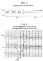
- the modulation causes the battery converter to operate for some fraction of the period and then disables the battery converter for the rest of the cycle, as shown in Figure 3. To produce a 60 Hz output waveform across the load, this modulation would be at a rate of 120 Hz.
- the transistors Q3 and Q4 operate in a push-pull configuration with a duty cycle of 50% during the ON portion.
- This second frequency is substantially higher than the line frequency.
- a typical operating frequency would be between 15 kHz and 100 kHz, and preferably 20 kHz.
- the transformer's secondary winding and rectifier will produce a DC voltage between nodes 12 and 14. This DC voltage is twice the desired output voltage "V".
- the voltage differential between nodes 12 and 14 may be 320 Volts DC (where the desired output voltage is 160 Volts).
- transistors Q1 and Q2 alternately conduct to apply the DC voltage to the load.
- the positive DC voltage terminal 12 is connected to neutral through resistor R1.
- the center tap of the high voltage winding is now at -V.
- This negative voltage is applied to the load node 16 for the duration of the ON period of the battery converter's operation.
- the battery converter is disabled, the voltage -V is actively removed from the load by simultaneous conduction of Q1 and Q2. This effectively shorts out the load and produces a low impedance zero. This is necessary for inductive loads to prevent the load voltage at node 16 from uncontrolled variations.
- the transistor Q1 is switched to a non-conductive state.
- the resistors R1 and R2 offer current protection to the transistors Q1 and Q2. During the low impedance zero and the charging of the output capacitor C, currents can flow that could damage the transistors.
- the resistors R1 and R2 inserted in the source connections of Q1 and Q2 will reduce the gate voltage just before damaging currents flow. The reduced gate voltage will cause the transistor to operate in the linear region, resulting in limited current in the transistors.
- the line voltage is applied through the transfer means 50 to the load.
- Transistors Q3 and Q4 are OFF.
- Q1 is turned ON.
- the line voltage is applied across winding 61 of inductor 60.
- a voltage equal to the voltage applied across winding 61, appears across winding 62 of inductor 60.
- This causes a current to flow through both transistors Q1 and Q2 to charge capacitor C2.
- current starts to increase in winding 61 of inductor 60.
- the diode D2 is reverse biased. The current will increase until the desired peak current is reached. At this desired current, the transistor Q1 is switched OFF.
- the transistor When the transistor is switched OFF, the voltage across the inductor reverses, causing the winding 63 of inductor 60 to forward bias diode D2. This allows the stored energy to be recovered by coupling it into the battery.
- the inductor current reaches a minimum current, the transistor Q1 turns on again and the cycle repeats as long as the line voltage is positive.
- the charger action can continue by using transistor Q2 to increase the current in winding 62 of inductor 60.
- the transistor Q2 is turned OFF and the winding 63 of inductor 60 conducts current through the diode D2 to recover the stored inductor energy.
- the high frequency transformer becomes saturated after repeated transistor conduction since there is no means to reset the core. This effectively removes this transformer from the circuit, essentially connecting the inductor 60 directly to the utility.
- switching device Q1 turns on at to with line voltage at node 12.
- Line voltage is applied across winding 61 of inductor 60.
- After C2 has charged ( t 1 ) we see current increase in winding 61 until Q1 turns off at t 2 .
- the stored energy in inductor 60 is released through winding 63 and diode D2 into the battery.
Landscapes
- Engineering & Computer Science (AREA)
- Power Engineering (AREA)
- Business, Economics & Management (AREA)
- Emergency Management (AREA)
- Charge And Discharge Circuits For Batteries Or The Like (AREA)
- Dc-Dc Converters (AREA)
- Stand-By Power Supply Arrangements (AREA)
- Inverter Devices (AREA)
- Amplifiers (AREA)
- Control Of Vehicles With Linear Motors And Vehicles That Are Magnetically Levitated (AREA)
Claims (8)
- Alimentation secourue (alimentation UPS) comportant des première et seconde bornes de sortie, destinée à générer une tension de sortie alternative, l'alimentation secourue comprenant :un transformateur (T) comportant un enroulement primaire et un enroulement secondaire,un convertisseur à basse tension (02), comprenant une batterie (B), fournissant une tension continue, couplé fonctionnellement par l'intermédiaire d'un premier moyen de commutation (Q3, Q4) audit enroulement primaire, pour générer une tension alternative sur ledit enroulement secondaire à partir de la batterie dans un premier mode de fonctionnement et pour découpler la batterie dudit enroulement primaire dans un second mode de fonctionnement,un circuit redresseur connecté audit enroulement secondaire, le circuit redresseur comportant des première et seconde bornes de sortie (12, 14),l'enroulement secondaire du transformateur comportant une borne centrale connectée à l'une desdites première et seconde bornes de sortie de l'alimentation secourue, etun moyen de transfert (50) pour connecter l'une desdites première et seconde bornes de sortie de l'alimentation secourue à une source d'alimentation en courant alternatif (SECTEUR) dans le second mode de fonctionnement,un onduleur à haute tension (01) relié aux première et seconde bornes de sortie (12, 14) du circuit redresseur et comprenant un second moyen de commutation (Q1, Q2) pour connecter, dans le premier mode de fonctionnement, l'une des bornes du circuit redresseur à l'autre desdites première et seconde bornes de sortie de l'alimentation secourue pour générer la tension de sortie alternative à partir de la tension générée aux première et seconde bornes de sortie (12, 14) du circuit redresseur, où un premier enroulement (61, 62) d'une bobine d'inductance (60) est agencé entre les première et/ou seconde bornes de sortie du circuit redresseur et le second moyen de commutation (Q1, Q2),où une liaison en série d'un second enroulement (63) de la bobine d'inductance (60) et d'une diode (D2) est connectée aux bornes de la batterie (B) et le au moins un premier enroulement (61, 62) de la bobine d'inductance est couplé magnétiquement au second enroulement (63), grâce à quoi, dans le second mode de fonctionnement, l'énergie stockée dans la bobine d'inductance (60) est transférée par l'intermédiaire d'un second enroulement (62) et d'une diode (D2) vers la batterie afin de charger la batterie.
- Alimentation secourue selon la revendication 1,
dans laquelle lesdits premier et second enroulements de bobine d'inductance sont couplés par induction mutuelle par l'intermédiaire d'un noyau commun. - Alimentation secourue selon la revendication 1 ou 2,
dans laquelle ledit second moyen de commutation (Q1, Q2) comporte une première borne d'entrée et une seconde borne d'entrée,
dans laquelle :un dit premier enroulement de bobine d'inductance (61) relie ladite première borne de sortie (12) dudit circuit redresseur à ladite première borne d'entrée dudit second moyen de commutation, et un autre dit premier enroulement de bobine d'inductance (62) relie ladite seconde borne de sortie (14) dudit circuit redresseur à ladite seconde borne d'entrée dudit second moyen de commutation. - Alimentation secourue selon la revendication 3,
dans laquelle ledit second moyen de commutation (Q1, Q2) agit pour connecter de façon alternée lesdites première et seconde bornes de sortie (12, 14) du circuit redresseur à l'autre desdites première et seconde bornes de sortie de l'alimentation UPS dans le premier mode de fonctionnement, afin de générer la tension de sortie alternative. - Alimentation secourue selon la revendication 3,
dans laquelle ledit moyen de transfert (50) est un commutateur qui connecte la source d'alimentation en courant alternatif audit enroulement secondaire du transformateur dans le second mode de fonctionnement, et dans laquelle ledit second moyen de commutation (Q1, Q2) agit pour connecter sélectivement ledit enroulement secondaire du transformateur aux bornes de sortie de l'alimentation UPS dans le second mode de fonctionnement, afin de transférer de l'énergie depuis la source d'alimentation en courant alternatif vers la batterie par l'intermédiaire des premier (61, 62) et second (63) enroulements de bobine d'inductance couplés. - Alimentation secourue selon la revendication 3,
dans laquelle ledit moyen de transfert (50) est un commutateur qui connecte l'une des première et seconde bornes de sortie de l'alimentation UPS et ladite borne centrale dudit enroulement secondaire du transformateur à la source d'alimentation en courant alternatif, dans le second mode de fonctionnement, et
dans laquelle ledit second moyen de commutation (Q1, Q2) agit pour connecter sélectivement lesdites première et seconde bornes de sortie (12, 14) dudit circuit redresseur à l'autre desdites première et seconde bornes de sortie de l'alimentation UPS dans le second mode de fonctionnement, afin de transférer de l'énergie depuis la source d'alimentation en courant alternatif vers la batterie par l'intermédiaire des premier (61, 62) et second (63) enroulements de bobine d'inductance. - Procédé de génération d'une tension de sortie alternative entre des première et seconde bornes de sortie d'une alimentation secourue (alimentation UPS) à partir d'une tension continue générée par une batterie (B) dans un premier mode de fonctionnement et à partir d'une source d'alimentation en courant alternatif (SECTEUR) dans un second mode de fonctionnement, le procédé comprenant les étapes consistant à :appliquer dans le premier mode de fonctionnement la tension continue par l'intermédiaire d'un premier moyen de commutation (Q3, Q4) avec une polarité alternée à des bornes d'extrémité d'un enroulement primaire d'un transformateur (T) afin de générer une tension alternative sur un enroulement secondaire du transformateur, l'enroulement secondaire comportant une borne centrale connectée à une première borne de sortie de l'alimentation UPS et découplant dans le second mode de fonctionnement la batterie de l'enroulement primaire du transformateur,appliquer la tension alternative sur l'enroulement secondaire du transformateur à un circuit redresseur pour générer des première et seconde tensions continues redressées à des première et seconde bornes de sortie (12, 14) du redresseur,relier de façon alternative, dans le premier mode de fonctionnement, les première et seconde bornes de sortie du redresseur par l'intermédiaire d'un second moyen de commutation (Q1, Q2) à la seconde borne de sortie de l'alimentation UPS à une première fréquence pour générer la tension de sortie alternative entre les bornes de sortie de l'alimentation UPS, où les première et/ou seconde bornes de sortie du redresseur sont reliées par l'intermédiaire d'un premier enroulement (61, 62) d'une bobine d'inductance (60) au second moyen de commutation (Q1, Q2),appliquer dans un second mode de fonctionnement la source d'alimentation en courant alternatif (SECTEUR) par l'intermédiaire d'un moyen de transfert (50) à la première borne de sortie de l'alimentation secourue, ettransférer dans le second mode de fonctionnement l'énergie stockée dans la bobine d'inductance (60) par l'intermédiaire d'un second enroulement (63) et d'une diode (D2) vers la batterie afin de charger la batterie, grâce à quoi le au moins un premier enroulement (61, 62) de la bobine d'inductance est couplé magnétiquement au second enroulement (63).
- Procédé selon la revendication 7, comprenant en outre l'étape consistant à relier simultanément les première et seconde bornes de sortie du redresseur à la seconde borne de sortie de l'alimentation UPS lorsque l'enroulement primaire du transformateur est découplé de la batterie.
Applications Claiming Priority (3)
| Application Number | Priority Date | Filing Date | Title |
|---|---|---|---|
| US98588897A | 1997-11-25 | 1997-11-25 | |
| US985888 | 1997-11-25 | ||
| PCT/US1998/024751 WO1999027630A1 (fr) | 1997-11-25 | 1998-11-18 | Circuits de charge pour alimentation electrique sans coupure |
Publications (2)
| Publication Number | Publication Date |
|---|---|
| EP1034597A1 EP1034597A1 (fr) | 2000-09-13 |
| EP1034597B1 true EP1034597B1 (fr) | 2005-08-17 |
Family
ID=25531888
Family Applications (1)
| Application Number | Title | Priority Date | Filing Date |
|---|---|---|---|
| EP98958657A Expired - Lifetime EP1034597B1 (fr) | 1997-11-25 | 1998-11-18 | Circuits de charge pour alimentation electrique sans coupure |
Country Status (10)
| Country | Link |
|---|---|
| US (1) | US6121756A (fr) |
| EP (1) | EP1034597B1 (fr) |
| JP (1) | JP4103946B2 (fr) |
| CN (1) | CN1197220C (fr) |
| AT (1) | ATE302491T1 (fr) |
| AU (1) | AU761505B2 (fr) |
| BR (1) | BR9815108A (fr) |
| CA (1) | CA2311529A1 (fr) |
| DE (1) | DE69831267T2 (fr) |
| WO (1) | WO1999027630A1 (fr) |
Families Citing this family (13)
| Publication number | Priority date | Publication date | Assignee | Title |
|---|---|---|---|---|
| US6400043B1 (en) * | 1998-11-30 | 2002-06-04 | American Power Conversion Corporation | Modular uninterruptable power supply |
| US6822425B2 (en) * | 2002-01-25 | 2004-11-23 | Vector Products, Inc. | High frequency battery charger and method of operating same |
| US6744643B2 (en) * | 2002-09-06 | 2004-06-01 | Phoenixtec Power Co., Ltd. | Push-pull booster circuit with a pair of inductors for coupling |
| US7187531B1 (en) * | 2003-03-20 | 2007-03-06 | Tyco Electronics Power Systems, Inc. | Transient suppressor and power converter employing the same |
| US7528579B2 (en) | 2003-10-23 | 2009-05-05 | Schumacher Electric Corporation | System and method for charging batteries |
| JP4859932B2 (ja) * | 2007-01-12 | 2012-01-25 | 株式会社明電舎 | 瞬時電圧低下・停電対策機能を有する電力変換システムの制御装置および制御方法 |
| CN102035393B (zh) * | 2010-12-17 | 2012-11-21 | 南京航空航天大学 | 四开关管三端口变换器 |
| US9537332B2 (en) | 2013-05-30 | 2017-01-03 | Canara, Inc. | Apparatus, system and method for charge balancing of individual batteries in a string of batteries using battery voltage and temperature, and detecting and preventing thermal runaway |
| US10120034B2 (en) | 2015-10-07 | 2018-11-06 | Canara, Inc. | Battery string monitoring system |
| DE112016006844T5 (de) * | 2016-05-12 | 2019-02-14 | Robert Bosch Gmbh | Batterietrennschaltungen und Verfahren zum Steuern einer Batterietrennschaltung |
| EP3772794A1 (fr) | 2019-08-08 | 2021-02-10 | Schneider Electric IT Corporation | Topologie de circuit de dispositifs d'alimentation à inducteurs couplés |
| KR102869817B1 (ko) * | 2019-10-04 | 2025-10-10 | 주식회사 엘지에너지솔루션 | 배터리 관리 장치 |
| US20240322696A1 (en) * | 2023-03-21 | 2024-09-26 | Sensata Technologies, Inc. | Isolated solid-state active pre-charger |
Family Cites Families (11)
| Publication number | Priority date | Publication date | Assignee | Title |
|---|---|---|---|---|
| FR2543357A1 (fr) * | 1983-03-25 | 1984-09-28 | Gagne Claude | Transformateur electrique de puissance de taille reduite permettant le controle des caracteristiques de la tension de sortie |
| US4641232A (en) * | 1985-01-23 | 1987-02-03 | Allied Corporation | Electrical power inverter having a phase modulated, twin-inverter, high frequency link and an energy storage module |
| US4639849A (en) * | 1985-05-08 | 1987-01-27 | International Exide Electronics/Corporation | Snubber circuit for H.F. bridge converter |
| US4706177A (en) * | 1985-11-14 | 1987-11-10 | Elliot Josephson | DC-AC inverter with overload driving capability |
| US4935861A (en) * | 1989-06-13 | 1990-06-19 | Exide Electronics | Uninterrupted power supply having no low frequency power magnetics |
| US5302858A (en) * | 1991-12-11 | 1994-04-12 | Best Power Technology, Incorporated | Method and apparatus for providing battery charging in a backup power system |
| US5291383A (en) * | 1992-09-02 | 1994-03-01 | Exide Electronics Corporation | Simplified UPS system |
| US5469098A (en) * | 1993-03-29 | 1995-11-21 | Exide Electronics Corporation | Isolated gate drive |
| US5555494A (en) * | 1993-09-13 | 1996-09-10 | Morris; George Q. | Magnetically integrated full wave DC to DC converter |
| US5648895A (en) * | 1995-12-19 | 1997-07-15 | Sysgration Ltd. | Flyback and charging circuitry for an uninterruptible power supply system |
| US5790391A (en) * | 1996-11-29 | 1998-08-04 | General Signal Corporation | Standby power system |
-
1998
- 1998-11-18 CA CA002311529A patent/CA2311529A1/fr not_active Abandoned
- 1998-11-18 AU AU14655/99A patent/AU761505B2/en not_active Ceased
- 1998-11-18 BR BR9815108-8A patent/BR9815108A/pt not_active IP Right Cessation
- 1998-11-18 JP JP2000522663A patent/JP4103946B2/ja not_active Expired - Fee Related
- 1998-11-18 EP EP98958657A patent/EP1034597B1/fr not_active Expired - Lifetime
- 1998-11-18 CN CNB988133040A patent/CN1197220C/zh not_active Expired - Fee Related
- 1998-11-18 AT AT98958657T patent/ATE302491T1/de not_active IP Right Cessation
- 1998-11-18 DE DE69831267T patent/DE69831267T2/de not_active Expired - Lifetime
- 1998-11-18 WO PCT/US1998/024751 patent/WO1999027630A1/fr not_active Ceased
-
1999
- 1999-10-25 US US09/426,347 patent/US6121756A/en not_active Expired - Fee Related
Also Published As
| Publication number | Publication date |
|---|---|
| BR9815108A (pt) | 2000-10-10 |
| CA2311529A1 (fr) | 1999-06-03 |
| WO1999027630A1 (fr) | 1999-06-03 |
| CN1302468A (zh) | 2001-07-04 |
| JP4103946B2 (ja) | 2008-06-18 |
| ATE302491T1 (de) | 2005-09-15 |
| CN1197220C (zh) | 2005-04-13 |
| US6121756A (en) | 2000-09-19 |
| AU761505B2 (en) | 2003-06-05 |
| AU1465599A (en) | 1999-06-15 |
| DE69831267T2 (de) | 2006-06-22 |
| JP2001524796A (ja) | 2001-12-04 |
| EP1034597A1 (fr) | 2000-09-13 |
| DE69831267D1 (de) | 2005-09-22 |
Similar Documents
| Publication | Publication Date | Title |
|---|---|---|
| US6504267B1 (en) | Flyback power converter with secondary-side control and primary-side soft switching | |
| JP2929178B2 (ja) | 循環電流低減型の高周波ソフトスイッチング・パルス幅変調フルブリッジdc/dcコンバータ | |
| US5896280A (en) | Frequency converter and improved UPS employing the same | |
| US5440179A (en) | UPS with bi-directional power flow | |
| USRE37889E1 (en) | Low loss synchronous rectifier for application to clamped-mode power converters | |
| CA2314782C (fr) | Convertisseurs d'alimentation multimode comportant des circuits d'equilibrage et methode de fonctionnement desdits appareils | |
| US6906930B2 (en) | Structure and method for an isolated boost converter | |
| US5448467A (en) | Electrical power converter circuit | |
| EP1034597B1 (fr) | Circuits de charge pour alimentation electrique sans coupure | |
| CN103580492A (zh) | 新式高功率变换器架构 | |
| EP0519649A2 (fr) | Convertisseur à un seul étage avec amélioration du facteur de puissance et sortie isolée | |
| JP4682482B2 (ja) | スイッチング電源回路 | |
| Eitzen et al. | Bidirectional power electronics for driving dielectric elastomer transducers | |
| WO2002007296A1 (fr) | Regulateur de commutation en courant continu | |
| KR200266522Y1 (ko) | 2-스위치포워드컨버터용에너지재생스너버회로 | |
| JPH11275860A (ja) | Dcーdcコンバータ | |
| CN121841090A (zh) | 限功率的谐振变换器和变流设备 | |
| Sneha et al. | DESIGN AND IMPLEMENTATION OF DC-DC CONVERTER WITH ZVS AND ZCS FOR VARIOUS INTERACTING LOADS | |
| Yilmaz | SMR 48 V/15 A forced cooling switchmode rectifier by using phase modulated control topology and integrated magnetic concept | |
| WO2001048899A2 (fr) | Convertisseur d'alimentation electrique commute a sorties multiples produisant une tension continue dans une sortie |
Legal Events
| Date | Code | Title | Description |
|---|---|---|---|
| PUAI | Public reference made under article 153(3) epc to a published international application that has entered the european phase |
Free format text: ORIGINAL CODE: 0009012 |
|
| 17P | Request for examination filed |
Effective date: 20000524 |
|
| AK | Designated contracting states |
Kind code of ref document: A1 Designated state(s): AT BE CH CY DE DK ES FI FR GB GR IE IT LI LU MC NL PT SE |
|
| 17Q | First examination report despatched |
Effective date: 20010709 |
|
| GRAP | Despatch of communication of intention to grant a patent |
Free format text: ORIGINAL CODE: EPIDOSNIGR1 |
|
| RAP1 | Party data changed (applicant data changed or rights of an application transferred) |
Owner name: EATON POWER QUALITY CORPORATION |
|
| GRAS | Grant fee paid |
Free format text: ORIGINAL CODE: EPIDOSNIGR3 |
|
| GRAA | (expected) grant |
Free format text: ORIGINAL CODE: 0009210 |
|
| AK | Designated contracting states |
Kind code of ref document: B1 Designated state(s): AT BE CH CY DE DK ES FI FR GB GR IE IT LI LU MC NL PT SE |
|
| PG25 | Lapsed in a contracting state [announced via postgrant information from national office to epo] |
Ref country code: NL Free format text: LAPSE BECAUSE OF FAILURE TO SUBMIT A TRANSLATION OF THE DESCRIPTION OR TO PAY THE FEE WITHIN THE PRESCRIBED TIME-LIMIT Effective date: 20050817 Ref country code: LI Free format text: LAPSE BECAUSE OF FAILURE TO SUBMIT A TRANSLATION OF THE DESCRIPTION OR TO PAY THE FEE WITHIN THE PRESCRIBED TIME-LIMIT Effective date: 20050817 Ref country code: IT Free format text: LAPSE BECAUSE OF FAILURE TO SUBMIT A TRANSLATION OF THE DESCRIPTION OR TO PAY THE FEE WITHIN THE PRESCRIBED TIME-LIMIT;WARNING: LAPSES OF ITALIAN PATENTS WITH EFFECTIVE DATE BEFORE 2007 MAY HAVE OCCURRED AT ANY TIME BEFORE 2007. THE CORRECT EFFECTIVE DATE MAY BE DIFFERENT FROM THE ONE RECORDED. Effective date: 20050817 Ref country code: FI Free format text: LAPSE BECAUSE OF FAILURE TO SUBMIT A TRANSLATION OF THE DESCRIPTION OR TO PAY THE FEE WITHIN THE PRESCRIBED TIME-LIMIT Effective date: 20050817 Ref country code: CH Free format text: LAPSE BECAUSE OF FAILURE TO SUBMIT A TRANSLATION OF THE DESCRIPTION OR TO PAY THE FEE WITHIN THE PRESCRIBED TIME-LIMIT Effective date: 20050817 Ref country code: BE Free format text: LAPSE BECAUSE OF FAILURE TO SUBMIT A TRANSLATION OF THE DESCRIPTION OR TO PAY THE FEE WITHIN THE PRESCRIBED TIME-LIMIT Effective date: 20050817 Ref country code: AT Free format text: LAPSE BECAUSE OF FAILURE TO SUBMIT A TRANSLATION OF THE DESCRIPTION OR TO PAY THE FEE WITHIN THE PRESCRIBED TIME-LIMIT Effective date: 20050817 |
|
| REG | Reference to a national code |
Ref country code: GB Ref legal event code: FG4D |
|
| REG | Reference to a national code |
Ref country code: CH Ref legal event code: EP |
|
| REG | Reference to a national code |
Ref country code: IE Ref legal event code: FG4D |
|
| REF | Corresponds to: |
Ref document number: 69831267 Country of ref document: DE Date of ref document: 20050922 Kind code of ref document: P |
|
| PG25 | Lapsed in a contracting state [announced via postgrant information from national office to epo] |
Ref country code: SE Free format text: LAPSE BECAUSE OF FAILURE TO SUBMIT A TRANSLATION OF THE DESCRIPTION OR TO PAY THE FEE WITHIN THE PRESCRIBED TIME-LIMIT Effective date: 20051117 Ref country code: GR Free format text: LAPSE BECAUSE OF FAILURE TO SUBMIT A TRANSLATION OF THE DESCRIPTION OR TO PAY THE FEE WITHIN THE PRESCRIBED TIME-LIMIT Effective date: 20051117 Ref country code: DK Free format text: LAPSE BECAUSE OF FAILURE TO SUBMIT A TRANSLATION OF THE DESCRIPTION OR TO PAY THE FEE WITHIN THE PRESCRIBED TIME-LIMIT Effective date: 20051117 |
|
| PG25 | Lapsed in a contracting state [announced via postgrant information from national office to epo] |
Ref country code: IE Free format text: LAPSE BECAUSE OF NON-PAYMENT OF DUE FEES Effective date: 20051118 Ref country code: CY Free format text: LAPSE BECAUSE OF FAILURE TO SUBMIT A TRANSLATION OF THE DESCRIPTION OR TO PAY THE FEE WITHIN THE PRESCRIBED TIME-LIMIT Effective date: 20051118 |
|
| PG25 | Lapsed in a contracting state [announced via postgrant information from national office to epo] |
Ref country code: ES Free format text: LAPSE BECAUSE OF FAILURE TO SUBMIT A TRANSLATION OF THE DESCRIPTION OR TO PAY THE FEE WITHIN THE PRESCRIBED TIME-LIMIT Effective date: 20051128 |
|
| PG25 | Lapsed in a contracting state [announced via postgrant information from national office to epo] |
Ref country code: MC Free format text: LAPSE BECAUSE OF NON-PAYMENT OF DUE FEES Effective date: 20051130 Ref country code: LU Free format text: LAPSE BECAUSE OF NON-PAYMENT OF DUE FEES Effective date: 20051130 |
|
| PG25 | Lapsed in a contracting state [announced via postgrant information from national office to epo] |
Ref country code: PT Free format text: LAPSE BECAUSE OF FAILURE TO SUBMIT A TRANSLATION OF THE DESCRIPTION OR TO PAY THE FEE WITHIN THE PRESCRIBED TIME-LIMIT Effective date: 20060117 |
|
| NLV1 | Nl: lapsed or annulled due to failure to fulfill the requirements of art. 29p and 29m of the patents act | ||
| REG | Reference to a national code |
Ref country code: CH Ref legal event code: PL |
|
| ET | Fr: translation filed | ||
| PLBE | No opposition filed within time limit |
Free format text: ORIGINAL CODE: 0009261 |
|
| STAA | Information on the status of an ep patent application or granted ep patent |
Free format text: STATUS: NO OPPOSITION FILED WITHIN TIME LIMIT |
|
| 26N | No opposition filed |
Effective date: 20060518 |
|
| REG | Reference to a national code |
Ref country code: IE Ref legal event code: MM4A |
|
| PGFP | Annual fee paid to national office [announced via postgrant information from national office to epo] |
Ref country code: DE Payment date: 20091130 Year of fee payment: 12 |
|
| PGFP | Annual fee paid to national office [announced via postgrant information from national office to epo] |
Ref country code: GB Payment date: 20091007 Year of fee payment: 12 Ref country code: FR Payment date: 20091120 Year of fee payment: 12 |
|
| GBPC | Gb: european patent ceased through non-payment of renewal fee |
Effective date: 20101118 |
|
| REG | Reference to a national code |
Ref country code: DE Ref legal event code: R119 Ref document number: 69831267 Country of ref document: DE Effective date: 20110601 Ref country code: DE Ref legal event code: R119 Ref document number: 69831267 Country of ref document: DE Effective date: 20110531 |
|
| REG | Reference to a national code |
Ref country code: FR Ref legal event code: ST Effective date: 20110801 |
|
| PG25 | Lapsed in a contracting state [announced via postgrant information from national office to epo] |
Ref country code: DE Free format text: LAPSE BECAUSE OF NON-PAYMENT OF DUE FEES Effective date: 20110531 |
|
| PG25 | Lapsed in a contracting state [announced via postgrant information from national office to epo] |
Ref country code: FR Free format text: LAPSE BECAUSE OF NON-PAYMENT OF DUE FEES Effective date: 20101130 |
|
| PG25 | Lapsed in a contracting state [announced via postgrant information from national office to epo] |
Ref country code: GB Free format text: LAPSE BECAUSE OF NON-PAYMENT OF DUE FEES Effective date: 20101118 |