EP1035516B1 - Système pour un module de sécurité - Google Patents
Système pour un module de sécurité Download PDFInfo
- Publication number
- EP1035516B1 EP1035516B1 EP00250055A EP00250055A EP1035516B1 EP 1035516 B1 EP1035516 B1 EP 1035516B1 EP 00250055 A EP00250055 A EP 00250055A EP 00250055 A EP00250055 A EP 00250055A EP 1035516 B1 EP1035516 B1 EP 1035516B1
- Authority
- EP
- European Patent Office
- Prior art keywords
- voltage
- battery
- security module
- line
- self
- Prior art date
- Legal status (The legal status is an assumption and is not a legal conclusion. Google has not performed a legal analysis and makes no representation as to the accuracy of the status listed.)
- Expired - Lifetime
Links
Images


Classifications
-
- G—PHYSICS
- G07—CHECKING-DEVICES
- G07B—TICKET-ISSUING APPARATUS; FARE-REGISTERING APPARATUS; FRANKING APPARATUS
- G07B17/00—Franking apparatus
- G07B17/00733—Cryptography or similar special procedures in a franking system
-
- G—PHYSICS
- G07—CHECKING-DEVICES
- G07B—TICKET-ISSUING APPARATUS; FARE-REGISTERING APPARATUS; FRANKING APPARATUS
- G07B17/00—Franking apparatus
- G07B17/00185—Details internally of apparatus in a franking system, e.g. franking machine at customer or apparatus at post office
- G07B17/00193—Constructional details of apparatus in a franking system
- G07B2017/00233—Housing, e.g. lock or hardened casing
-
- G—PHYSICS
- G07—CHECKING-DEVICES
- G07B—TICKET-ISSUING APPARATUS; FARE-REGISTERING APPARATUS; FRANKING APPARATUS
- G07B17/00—Franking apparatus
- G07B17/00185—Details internally of apparatus in a franking system, e.g. franking machine at customer or apparatus at post office
- G07B17/00193—Constructional details of apparatus in a franking system
- G07B2017/00266—Man-machine interface on the apparatus
- G07B2017/00298—Visual, e.g. screens and their layouts
-
- G—PHYSICS
- G07—CHECKING-DEVICES
- G07B—TICKET-ISSUING APPARATUS; FARE-REGISTERING APPARATUS; FRANKING APPARATUS
- G07B17/00—Franking apparatus
- G07B17/00185—Details internally of apparatus in a franking system, e.g. franking machine at customer or apparatus at post office
- G07B17/00193—Constructional details of apparatus in a franking system
- G07B2017/00266—Man-machine interface on the apparatus
- G07B2017/00306—Acoustic, e.g. voice control or speech prompting
-
- G—PHYSICS
- G07—CHECKING-DEVICES
- G07B—TICKET-ISSUING APPARATUS; FARE-REGISTERING APPARATUS; FRANKING APPARATUS
- G07B17/00—Franking apparatus
- G07B17/00185—Details internally of apparatus in a franking system, e.g. franking machine at customer or apparatus at post office
- G07B17/00314—Communication within apparatus, personal computer [PC] system, or server, e.g. between printhead and central unit in a franking machine
- G07B2017/00346—Power handling, e.g. power-down routine
-
- G—PHYSICS
- G07—CHECKING-DEVICES
- G07B—TICKET-ISSUING APPARATUS; FARE-REGISTERING APPARATUS; FRANKING APPARATUS
- G07B17/00—Franking apparatus
- G07B17/00733—Cryptography or similar special procedures in a franking system
- G07B2017/00959—Cryptographic modules, e.g. a PC encryption board
- G07B2017/00967—PSD [Postal Security Device] as defined by the USPS [US Postal Service]
Definitions
- the invention relates to an arrangement for a security module, according to the type specified in the preamble of claim 1.
- a postal security module is particularly suitable for use in a postage meter or mail processing machine or computer with mail processing function.
- Modern franking machines like those from the US 4,746,234 known thermal transfer postage meter, employ a fully electronic digital printing device.
- Applicants' T1000 meter has a microprocessor surrounded by a secure housing having an opening for delivering a letter.
- a mechanical letter sensor microwaveswitch
- the franking imprint includes previously entered and stored postal information for conveying the letter.
- the control unit of the franking machine carries out a software billing, exercises a monitoring function, possibly with regard to the conditions for a data update, and controls the reloading of a port value credit.
- thermal transfer franking machine has already been in US 5,606,508 ( DE 42 13 278 B1 ) and in US 5,490,077 proposed a data entry option using smart cards.
- One of the smart cards loads new data into the postage meter machine and a set of further smart cards allows a setting to be made according to stored data by inserting a chip card.
- the data loading and the setting of the franking machine can thus be more convenient and faster than by keyboard input.
- a franking machine for franking mail is provided with a printer for printing the postage stamp on the mail, a controller for controlling the printing and peripheral components of the postage meter, a bill unit for settling postage, at least one nonvolatile memory for storing postage data , equipped with at least one non-volatile memory for storing safety-relevant data and with a calendar / clock.
- the non-volatile memory of the safety-related data and / or the calender / clock is usually powered by a battery.
- security-relevant data (cryptographic keys and the like) are saved in nonvolatile memories. These memories are EEPROM, FRAM or battery backed SRAM.
- Known franking machines often also have an internal real time clock (RTC), which is powered by a battery.
- RTC real time clock
- encapsulated modules containing integrated circuits and a lithium battery. These modules must be replaced and disposed of at the end of the life of the battery as a whole. From an economic and ecological point of view, it is better if only the battery needs to be replaced. For this purpose, however, the security case must be opened and then closed again and sealed, because the security against fraud is essentially based on the secure housing, which encloses the entire machine.
- any required repair of a franking machine is then difficult on site, if the access to the components is difficult or limited.
- the secured housing will in future be reduced to the so-called postal security module, which may improve the accessibility to the other components.
- the battery of the security module it would also be desirable that they can be replaced in a relatively simple way. But then the battery would be outside the security area of the franking machine.
- a potential attacker is able to manipulate the battery voltage.
- Known battery-powered SRAMs and RTCs have different requirements with regard to their required operating voltage. The voltage required to hold data from SRAMs is below the required voltage for operating RTCs.
- the remote data center specifies a time credit or a period of time, in particular a number of days, or a specific day up to which the franking device is to report by means of a communication connection. After the time credit has expired or the deadline expires, franking is prevented.
- Security modules are already known from electronic data processing systems ago. To protect against burglary in an electronic system is in EP 417 447 B1 already proposed a lock, which includes power supply and signal detection means and shielding in the housing.
- the shielding means is made of encapsulating material and conductive means to which the power supply and signal detection means are connected. The latter responds to a change in the line resistance of the line means.
- the security module includes an internal battery, a voltage switch from system voltage to battery voltage and other functional units (such as power gate, short-circuit transistor, memory and sensors). When the voltage falls below a certain limit, the Power Gate responds. If the line resistance, temperature or radiation is changed, the logic will react.
- the output of the short-circuit transistor is switched to L level, whereby a memory stored in the cryptographic key is deleted.
- the life of the non-replaceable battery and thus of the security module for use in franking devices or mail processing machines is too small.
- a larger mail processing machine is, for example, the JetMail®.
- a franking print is here produced by means of a stationary ink jet printhead in a non-horizontal approximately vertical letter transport.
- a suitable design for a printing device was already in the DE 196 05 015 C1 proposed.
- the mailing machine has a meter and a base. If the meter is to be equipped with a housing so that components are more easily accessible, then it must be protected by a postal security module fraud attempts, which at least performs the settlement of postal fees.
- To exclude influences on the program has already been in the EP 789 333 A2 proposed to provide a security module with a user circuit (ASIC), which has a hardware A réelleaji.
- the user circuitry (ASIC) also controls the transfer of print data to the printhead.
- the security module not powered by a system voltage, could then be manipulated via the externally accessible battery contacts by reducing the voltage below the limit voltage specified for the processor. If the processor is equipped with an internal clock RAM (RTC), the clock will stop first. Increasing the voltage would cause the internal clock (RTC) to continue running.
- RTC internal clock RAM
- the DE 44 10 338 A shows a data transmission system with a transmitting unit, which has two operating modes: In normal operation, a supply of the transmitting unit with the main energy source, while in emergency mode, an internal or external energy source is switched on.
- the invention has for its object to ensure the security against unauthorized manipulation of a security module when the battery is arranged interchangeable.
- a postal device in particular a franking machine, is equipped with a plug-in security module, which is connected to the system bus of the meter or another suitable control device.
- a plug-in security module which is supplied by a system voltage at the time of service, the battery of the safety module can be replaced by a service technician.
- the security module is potted with a hard mass. For a battery change or disposal, however, the battery is located outside the potting compound.
- the security module has a voltage monitoring unit with resettable latching, which can be queried and reset by the processor.
- Monitoring the voltage of a battery which is required for the battery-backed RAM memory and for the function of an internal clock, has the aim of triggering actions that result in the deletion of safety-relevant data and the current time when the voltage falls below a certain voltage level. Latching allows preserving the state of the voltage underrun until reliable detection is possible. The latter is only later the case when the module is supplied with system voltage again. An inspector or other authorized person who makes appropriate entries on the keypad of the franking device can restore the original condition.
- the advantages in addition to extending the life of the security module by the possibility of battery replacement, are in a low power consumption of the circuit despite a rapid response to voltage changes and prevention of averaging in a manipulation with square pulses on the battery terminals.
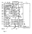
- FIG. 1 is a block diagram of the security module 100 with the contact groups 101, 102 for connection to an interface 8 and with the battery contact terminals 103 and 104 of a battery interface for a battery 134 shown.
- the security module 100 is potted with a hard potting compound, the battery 134 of the security module 100 is interchangeably disposed outside of the potting compound on a printed circuit board.
- the circuit board carries the battery contact terminals 103 and 104 for connecting the poles of the battery 134.
- the security module 100 is plugged into a corresponding interface 8 of the motherboard (motherboard) 9.
- the first contact group 101 communicates with the system bus of a control device and the second contact group 102 serves to supply the security module 100 with the system voltage.
- the first and / or second contact group 101 and / or 102 are / is designed for static and dynamic monitoring of the plugged in the security module 100.
- the supply of the security module 100 is realized with the system voltage of the motherboard 9 and via the pins P1, P2 or P4, a dynamic and static unplugged detection is realized by the security module 100.
- the security module 100 has, in a manner known per se, a microprocessor 120 which contains an integrated read-only memory (internal ROM) with the special application program (not shown), which is approved for the franking machine by the postal authority or the respective mail carrier. Alternatively, a conventional read-only memory ROM or FLASH memory can be connected to the module-internal data bus 126.
- the security module 100 has, in a manner known per se, a reset circuit unit 130, a user circuit ASIC 150 and a logic PAL 160 which serves as the control signal generator for the ASIC.
- the reset circuit unit 130 or the user circuit ASIC 150 and the logic PAL 160 as well as possibly further - not shown - memory are supplied via the lines 191 and 129 with system voltage Us +, which is supplied from the motherboard 9 with the franking device turned on.
- system voltage Us + which is supplied from the motherboard 9 with the franking device turned on.
- PSM postal security module
- the system voltage Us + is also applied via a diode 181 and the line 136 at the input of the voltage monitoring unit 12.
- a second operating voltage U b + is supplied, which is available via the line 138.
- the negative terminal battery contact terminal 104 is connected to ground. From the battery contact terminal 103 lying on the positive pole, battery voltage is supplied via a line 193, via a second diode 182 and the line 136 to the input of the voltage monitoring unit.
- a commercial circuit can be used as a voltage switch 180.
- the output of the voltage monitoring unit 12 is via a line 138 with an input for this second operating voltage U b + connected to the processor 120, which at least leads to a RAM memory area 122, 124 and there guarantees a non-volatile storage as long as the second operating voltage U b + applied at the required height.
- the processor 120 preferably includes an internal RAM 124 and a real-time clock (RTC) 122.
- the voltage monitoring unit 12 in the security module 100 has a resettable latching, which can be queried by the processor 120 via a line 164 and reset via a line 135.
- the voltage monitoring unit 12 has circuit means, wherein the reset is triggered only when the battery voltage has risen above the predetermined threshold.
- the resettable latching will later on the basis of FIG. 5 explained in more detail.
- the lines 135 and 164 are each connected to a terminal (pin 1 and 2) of the processor 120.
- Line 164 provides a status signal to processor 120, and line 135 provides a control signal to voltage monitoring unit 12.
- the line 136 at the input of thecertainsüberwchungstician 12 also supplies a detection unit 13 with operating or battery voltage.
- the processor 120 queries the state of the detection unit 13 via the line 139 or the detection unit 13 is triggered or set by the processor 120 via the line 137. After setting, a static check is made for connection.
- ground potential is queried via a line 192, which is present at the connection P4 of the interface 8 of the postal security module PSM 100 and can only be interrogated when the security module 100 is inserted correctly.
- ground potential of the negative pole 104 of the battery 134 of the postal security module PSM 100 is placed on the port P23 of the interface 8 and is thus interrogated at port P4 of the interface 8 via the line 192 of the detection unit 13.
- a line loop which is looped back to the processor 120 via the pins P1 and P2 of the contact group 102 of the interface 8.
- the processor 120 changing signal levels at irregularly spaced intervals to the pins 6, 7 and looped back over the loop.
- FIG. 2 shows a block diagram of a postage meter, which is equipped with a chip card read / write unit 70 for reloading change data by chip card and with a printing device 2, which is controlled by a control device 1.
- the control device 1 has a motherboard 9 equipped with a microprocessor 91 with associated memories 92, 93, 94, 95.
- the program memory 92 contains an operating program for at least printing and at least safety-related components of the program for a predetermined format change of a portion of the user data.
- the RAM RAM 93 is used for volatile intermediate storage of intermediate results.
- NVM 94 non-volatile memory is used for non-volatile caching of data, such as statistical data organized by cost center.
- the calendar / clock module 95 also contains addressable but non-volatile memory areas for the non-volatile intermediate storage of intermediate results or also known program parts (for example for the DES algorithm).
- control device 1 is connected to the chip card write / read unit 70, wherein the microprocessor 91 of the control device 1 is programmed, for example, to load the payload N from the memory area of a chip card 49 for their application in corresponding memory areas of the franking machine ,
- a first chip card 49 inserted in a slot 72 of the chip card write / read unit 70 allows reloading of a record in the postage meter machine for at least one application.
- the chip card 49 contains, for example, the postage for all the usual postal carrier services according to the tariff of the postal authority and a post carrier code to generate a stamp image with the franking machine and to stamp the postal items according to the tariff of the postal authority.
- the control device 1 forms the actual meter with the means 91 to 95 of the aforementioned motherboard 9 and also includes a keyboard 88, a display unit 89 and an application-specific circuit ASIC 90 and the interface 8 for the postal security module PSM 100.
- the security module PSM 100 is via a control bus with the aforementioned ASIC 90 and the microprocessor 91 and the parallel ⁇ C bus at least with the means 91 to 95 of the motherboard 9 and with Display unit 89 connected.
- the control bus carries lines for the signals CE, RD and WR between the security module PSM 100 and the aforementioned ASIC 90.
- the microprocessor 91 preferably has a pin for an output from the security module PSM 100 interrupt signal i, other connections for the keyboard 88, a serial interface Sl-1 for the connection of the chip card read / write unit 70 and a serial interface Sl-2 for the optional connection of a MODEM.
- the MODEM for example, the credit stored in the non-volatile memory of the postal security device PSM 100 can be increased.
- the postal security device PSM 100 is surrounded by a secured housing. Before each franking imprint, a hardware settlement is carried out in the postal security module PSM 100. Billing is independent of cost centers.
- the postal security agent PSM 100 can be designed internally as in the European application EP 789 333 A3 was described in more detail.
- the ASIC 90 may include a serial interface circuit 98 to a post-stream powered device, a serial interface circuit 96 to the sensors and actuators of the printing device 2, a serial interface circuit 97 to the print control electronics 16 for the printhead 4, and a serial interface circuit 99 to one has the printing device 20 in the post-stream downstream device.
- a serial interface circuit 98 to a post-stream powered device a serial interface circuit 96 to the sensors and actuators of the printing device 2
- a serial interface circuit 97 to the print control electronics 16 for the printhead 4 and a serial interface circuit 99 to one has the printing device 20 in the post-stream downstream device.
- the peripheral interface can be removed, which is suitable for multiple peripheral devices (stations). It is entitled: Arrangement for communication between a base station and other stations of a mailing machine and their emergency shutdown.
- the interface circuit 96 coupled to the machine base interface circuit 14 provides at least one connection to the sensors 6, 7, 17 and to the actuators, such as the drive motor 15 for the roller 11 and a cleaning and sealing station RDS 40 for the ink jet printhead 4 , as well as to Labeler 50 in the machine base ago.
- the basic arrangement and the interaction between the inkjet printhead 4 and the RDS 40 are the DE 197 26 642 C2 removable, entitled: Arrangement for positioning an ink jet printhead and a cleaning and sealing device.
- the transport device consists of a conveyor belt 10 and two rollers 11,11 '.
- One of the rollers is equipped with a motor 15 drive roller 11, another is the follower tension roller 11 '.
- the drive roller 11 is designed as a toothed roller, according to the conveyor belt 10 is designed as a toothed belt, which ensures the unambiguous power transmission.
- An encoder 5, 6 is coupled to one of the rollers 11, 11 '.
- the drive roller 11 is firmly seated with an incremental encoder 5 on an axis.
- the incremental encoder 5 is designed, for example, as a slotted disk, which interacts with a light barrier 6, and outputs an encoder signal to the motherboard 9 via the line 19.
- the individual printing elements of the print head are connected within its housing with a print head electronics and that the print head for a purely electronic pressure can be controlled.
- the pressure control is based on the path control, whereby the selected stamp offset is taken into account, which is entered by keyboard 88 or if necessary by chip card and stored in memory NVM 94 non-volatile.
- a planned imprint thus results from stamp offset (without printing), the franking print image and possibly further print images for advertising clichés, shipping information (optional prints) and additional editable messages.
- the nonvolatile memory NVM 94 has a plurality of memory areas. These include those which save the loaded postage fee tables non-volatile.
- the chip card read / write unit 70 consists of an associated mechanical support for the microprocessor card and contact unit 74. The latter allows a secure mechanical support of the chip card in the read position and clear signaling of reaching the Reading position of the chip card in the contacting unit.
- the microprocessor card with the microprocessor 75 has a programmed read capability for all types of memory cards or smart cards.
- the interface to the franking machine is a serial interface in accordance with the RS232 standard.
- the data transfer rate is min. 1.2 K baud.
- the power supply is switched on by means of a switch 71 connected to the mainboard. After the power supply has been switched on, a self-test function with a ready message takes place.
- FIG. 3 is a perspective view of the postage meter from behind.
- the franking machine consists of a meter 1 and a base 2.
- the latter is equipped with a smart card write / read unit 70, which is arranged behind the guide plate 20 and accessible from the housing upper edge 22.
- a chip card 49 is inserted from top to bottom in the insertion slot 72.
- a supplied standing on the edge letter 3, which rests with its surface to be printed on the guide plate is then printed according to the input data with a franking stamp 31.
- the letter feeding opening is bounded laterally by a transparent plate 21 and the guide plate 20.
- the status display of the security module 100 inserted on the motherboard 9 of the meter 1 is visible from the outside through an opening 109.
- the FIG. 4 shows a block diagram of the postal security module PSM 100 in a preferred variant.
- the negative pole of the battery 134 is connected to ground and a pin P23 of the contact group 102.
- the positive pole of the battery 134 is connected to the one input of the voltage changeover switch 180 via the line 193, and the system voltage leading line 191 is connected to the other input of the voltage changeover switch 180.
- battery 134 is the type SL-389 / P for a lifetime up to 3.5 years or the type SL-386 / P for a lifetime up to 6 years with a maximum power consumption by the PSM 100 is suitable as a voltage switch 180, a commercial circuit of the type ADM 8693ARN be used.
- the output of the voltage changeover switch 180 is connected via the line 136 to the battery monitoring unit 12 and the detection unit 13.
- the battery monitoring unit 12 and the detection unit 13 communicate with the pins 1, 2, 4 and 5 of the processor 120 via the lines 135, 164 and 137, 139 in communication.
- the output of the Voltage changeover switch 180 is also connected via line 136 to the supply input of a first memory SRAM which, through the existing battery 134, becomes the non-volatile memory NVRAM of a first technology.
- the security module communicates with the postage meter via the system bus 115, 117, 118.
- the processor 120 may communicate via the system bus and a modem 83 in communication with a remote data center. Billing is completed by the ASIC 150.
- the postal billing data is stored in non-volatile memory of different technology.
- a second memory NV-RAM 114 system voltage is applied.
- This is a non-volatile memory NVRAM of a second technology, (SHADOW-RAM).
- This second technology preferably comprises a RAM and an EEPROM, the latter automatically assuming the data contents in the event of system voltage failure.
- the NVRAM 114 of the second technology is connected to the corresponding address and data inputs of the ASIC 150 via an internal address and data bus 112, 113.
- the ASIC 150 contains at least one hardware abort unit for the calculation of the postal data to be stored.
- Programmable Array Logic (PAL) 160 accommodates access logic to ASIC 150.
- the ASIC 150 is controlled by the PAL 160 logic.
- An address and control bus 117, 115 from the motherboard 9 is connected to corresponding pins of the PAL 160 logic and the PAL 160 generates at least a control signal for the ASIC 150 and a control signal 119 for the program memory FLASH 128.
- the processor 120 executes a program stored in the FLASH 128.
- Processor 120, FLASH 28, ASIC 150, and PAL 160 are interconnected via a module-internal system bus that includes lines 110, 11, 12, 126, 119 for data, address, and control signals.
- the RESET unit 130 is connected via the line 131 to the pin 3 of the processor 120 and to a pin of the ASIC 150.
- the processor 120 and the ASIC 150 are reset by a reset generation in the RESET unit 130 when the supply voltage drops.
- the real-time clock RTC 122 and the memory RAM 124 are supplied by an operating voltage via the line 138. This voltage is generated by the voltage monitoring unit (Battery Observer) 12. The latter also provides status signal 164 and responds to a control signal 135. Voltage selector 180, as an output voltage on line 136 for voltage monitor 12 and memory 116, forwards that of its input voltages which is greater than the other.
- the processor 120 internally has a processing unit CPU 121, a real time clock RTC 122, a RAM unit 124, and an input / output unit 125.
- a processing unit CPU 121 a real time clock RTC 122, a RAM unit 124, and an input / output unit 125.
- I / O ports of the input / output unit 125 to which module-internal signaling means are connected, for example, colored light emitting diode LED's 107, 108, which signal the state of the security module 100.
- the safety modules can assume different states in their life cycle. So, for example, to detect whether the module contains valid cryptographic keys. Furthermore, it is also important to distinguish whether the module is working or is defective. The exact type and number of module states depends on the implemented functions in the module and on the implementation.
- the processor 120 of the security module 100 is connected via a module-internal data bus 126 to a FLASH 128 and to the ASIC 150.
- the FLASH 128 serves as a program memory and is supplied with system voltage Us +. For example, it is a 128 Kbyte FLASH memory type AM29F010-45EC.
- the ASIC 150 of the postal security module 100 supplies addresses 0 to 7 to the corresponding address inputs of the FLASH 128 via a module-internal address bus 110.
- the processor 120 of the security module 100 delivers the addresses 8 to 15 to the corresponding address inputs of the FLASH 128 via an internal address bus 111
- the ASIC 150 of the security module 100 is connected via the contact group 101 of the interface 8 to the data bus 118, to the address bus 117 and to the control bus 115 of the motherboard 9 in communication connection.
- the real-time clock 122 with date and / or time registers and / or the static RAM (SRAM) 124 which holds security-related data When the voltage of the battery drops below a certain limit during battery operation, the supply point for RTC and SRAM is connected to ground by the circuit described in the exemplary embodiment. That the voltage at the RTC and at the SRAM is then at 0V. This results in the SRAM 124, e.g. contains important cryptographic keys, is deleted very quickly. At the same time, the registers of RTC 122 are cleared and the current time and date are lost. This action prevents a potential attacker from stopping the postage meter internal clock 122 by manipulating the battery voltage without losing any security related data. This prevents it from bypassing security measures such as long-time watchdogs.
- SRAM static RAM
- the described circuit changes into a self-holding state in which it remains even when subsequently increasing the voltage.
- the processor can query the state of the circuit (status signal) and thus and / or via the evaluation of the contents of the erased memory, conclude that the battery voltage has in the meantime fallen below a certain value.
- the processor may reset the monitor circuit, i. "make sharp.
- the circuit diagram of the voltage monitoring unit (Batterieobserver) 12 is explained.
- the circuit is powered by the battery voltage on line 136.
- a transistor 1252 is disabled and via the resistor 1254, the battery voltage on the line 138 as the operating voltage for Real-time clock RTC 122 or memory RAM 124 provided.
- the line 138 is the feed line for the RTC 122 and the RAM 124.
- the voltage monitoring unit 12 includes a voltage divider 1242, 1244 between the line 136 and ground having a tap 1246, that at the tap the inverting input of a comparator 1250, one of the latching means 1258 and one of the circuit means 1260 for a reset of the latch is connected.
- the output of the comparator 1250 is connected via an inverter 1252, 1254 on the one hand to the line 138 and on the other hand to the other circuit means 1256 for latching.
- the latter is a diode which returns L level to the tap.
- the voltage divider consists of two resistors 1242 and 1244 and a capacitor 1272 connected between tap and ground.
- the branch 1246 at the node of the two resistors 1242 and 1244 is connected to the inverting input of a comparator 1250.
- the noninverting input of the comparator 1250 is connected to a reference voltage source 1248.
- the output of the comparator 1250 is fed to the control input of a transistor 1252, which is connected to ground and connected to a line 136 located on the resistor 1254, that is connected as an inverter.
- the output of the inverter 1252, 1254 is connected to the line 138 and the n-type region of the diode 1256, whose p-type region is connected to the branch 1246 via a resistor 1258.
- a second transistor 1260 is connected in parallel with the resistor 1242, whose control input is connected to the line 135.
- the battery voltage on line 136 is reduced by a voltage divider comprised of two resistors 1242 and 1244 and a capacitor 1272 and compared by a comparator 1250 to the reference voltage of reference voltage source 1248. If the voltage to be compared on the branch 1246 is smaller than the reference voltage, the transistor 1252 receives H level at its control input and is turned on. As a result, the line 138 is connected to ground potential and the RTC 122 and the RAM 124 are no longer supplied with the battery voltage. As a result, the registers of the RTC 122 and the data in the RAM 124 are cleared and the RTC 122 stops.
- the monitoring circuit 12 changes to a self-holding state, in which it remains on the line 136 even when the voltage increases, leaving the line 138 at ground potential.
- an L signal is applied to the line 164 via a decoupling diode 1262, which can be queried by the processor 120.
- the decoupling diode 1262 serves to reduce the power consumption during battery operation.
- the processor 120 may reset the monitoring circuit 12. To do so, an H reset signal is applied to transistor 1260 via line 135, which is turned on.
- comparator 1250 switches back, and transistor 1252 is turned off.
- comparator 1250 the type ICL7665SAIBA is suitable.
- a diode 1268 decouples the supply voltage for the comparator 1250 from the battery voltage.
- An electrolytic capacitor 1270 ensures that the comparator 1250 is supplied with the supply voltage over a relatively long period of time (> 2 s), in which its function is ensured even though the battery voltage on the line 136 has been switched off.
- the circuit 12 is dimensioned so that any decrease in the battery voltage on the line 136 below the specified threshold of 2.6 V leads to the response of the circuit 12.
- the FIG. 6 shows the mechanical structure of the safety module in side view.
- the security module is designed as a multi-chip module, that is, a plurality of functional units are interconnected on a printed circuit board 106.
- the security module 100 is potted with a hard potting compound 105, wherein the battery 134 of the security module 100 is arranged outside of the potting compound 105 on a printed circuit board 106 interchangeable. For example, it is potted with a potting material 105 that signal means 107, 108 protrude from the potting material at a first location and that the circuit board 106 protrudes laterally with the inserted battery 134 a second location.
- the circuit board 106 also has battery contact terminals 103 and 104 for connecting the poles of the battery 134, preferably on the component side above the circuit board 106. It is envisaged that for plugging the postal security module PSM 100 on the motherboard of the meter 1, the contact groups 101 and 102 below the circuit board 106 (trace side) of the security module 100 are arranged.
- the user circuit ASIC 150 is via the first contact group 101 - in a manner not shown - in communication with the system bus of a control device 1 and the second contact group 102 serves to supply the security module 100 with the system voltage. If the security module is plugged onto the motherboard, then it is preferably arranged within the meter housing in such a way that the signal means 107, 108 near an opening 109 or projects into this.
- the meter housing is thus advantageously designed so that the user can still see the status of the security module from the outside.
- the two light emitting diodes 107 and 108 of the signal means are controlled via two output signals of the I / O ports to the pin 8, 9 of the processor 120.
- Both LEDs are housed in a common component housing (Bicolorleuchtdiode), which is why the dimensions or the diameter of the opening can remain relatively small and is of the order of the signal means. In principle, three different colors can be displayed (red, green, orange), of which only two are used (red and green).
- the LEDs are also used flashing, so that different state groups can be distinguished, which are characterized, for example, by the following LED states: LED off, LED flashing red, LED red, LED green flashing, LED green.
- FIG. 7 is a plan view of the postal security module shown.
- the FIGS. 8a or 8b show a view of the security module respectively from the right and from the left.
- the location of the contact groups 101 and 102 below the printed circuit board 106 is from the FIGS. 8a and 8b combined with FIG. 6 clear.
- the postal device in particular a franking machine
- the security module can also have a different design, which makes it possible, for example, it can be plugged onto the motherboard of a personal computer, which drives a commercial printer as a PC meter.
Landscapes
- Engineering & Computer Science (AREA)
- Theoretical Computer Science (AREA)
- Physics & Mathematics (AREA)
- General Physics & Mathematics (AREA)
- Devices For Checking Fares Or Tickets At Control Points (AREA)
- Management, Administration, Business Operations System, And Electronic Commerce (AREA)
- Analogue/Digital Conversion (AREA)
Claims (9)
- Disposition pour un module de sécurité équipé d'au moins une unité fonctionnelle (120), une batterie (134) et de dispositifs d'alimentation en tension de système et avec un commutateur de tension (180) qui est raccordé par une ligne (136) à une unité de contrôle de tension (12), laquelle fournit une tension de service à une mémoire (122, 124) via une ligne (138). La batterie (134) est disposée amovible sur le module de sécurité (100) et l'unité de contrôle de tension (12) présente des moyens de commutation (1256, 1258, 1260) pour un auto-maintien réinitialisable. Ledit auto-maintien est déclenché lorsque la tension de la batterie baisse en-dessous d'un seuil prédéterminé.
- Disposition selon la revendication 1, caractérisée en ce que l'unité de contrôle de tension (12) en tant que moyen de commutation présente une ligne (135) et un dispositif de commutation (1260) pour une réinitialisation de l'auto-maintien. Ladite réinitialisation est déclenchée uniquement lorsque la tension de la batterie a dépassé le seuil prédéterminé.
- Disposition selon l'une quelconque des revendications 1 à 2, caractérisée en ce que l'unité de contrôle de tension (12) comporte un diviseur de tension (1242, 1244) entre la ligne (136) et la masse, présentant un branchement (1246). L'entrée d'inversion d'un comparateur (1250) du moyen de commutation (1258) pour l'auto-maintien et le dispositif de commutation (1260) pour une réinitialisation de l'auto-maintien est branché à la prise. La sortie du comparateur (1250) est raccordée via un inverseur (1252, 1254) à la ligne (138) d'un côté et à l'autre moyen de commutation (1256) pour l'auto-maintien de l'autre.
- Disposition selon la revendication 3, caractérisée en ce que l'autre moyen de commutation de l'auto-maintien est une diode.
- Disposition selon la revendication 3, caractérisée en ce que l'entrée non inverseuse du comparateur (1250) est reliée à une source de tension de référence (1248).
- Disposition selon la revendication 3, caractérisée en ce que l'état de l'auto-maintien peut être appelé via une ligne (164) par un processeur (120) du module de sécurité (100).
- Disposition selon l'une quelconque des revendications 1 à 6, caractérisée en ce que le processeur (120) présente une mémoire (122, 124), à laquelle est amenée une tension de service par l'unité de contrôle de tension (12) via la ligne (138). Ledit processeur (120) est alimenté en tension de système et présente un premier Pin1, afin de réinitialiser l'état de l'auto-maintien par une ligne (135). Il présente également un second Pin2, auquel est raccordé la ligne (164), afin d'interroger l'état de l'unité de contrôle de tension (12), si elle est branchée sur décharge de tension de service ou sur auto-maintien.
- Disposition selon la revendication 7, caractérisée en ce que le module de sécurité (100) présente un circuit de commutation utilisateur ASIC (150). Le processeur (120) est relié via un bus de données à l'intérieur du module (126) au circuit de commutation utilisateur ASIC (150), ce dernier restant en liaison de communication avec le bus de systèmes d'un dispositif de commande (1) via un premier groupe de contact (101).
- Disposition selon la revendication 1, caractérisée en ce que le module de sécurité (100) est scellé avec une masse de coulage (105) dure. La batterie (134) du module de sécurité (100) est disposée amovible en dehors de la masse de coulage (105) sur une plaquette (106). Ladite plaquette (106) présente des bornes de contact de batterie (103 et 104) pour le raccord du pôle de la batterie (134) et un second groupe de contact (102) pour l'alimentation en tension de système du module de sécurité (100).
Applications Claiming Priority (2)
| Application Number | Priority Date | Filing Date | Title |
|---|---|---|---|
| DE19912780A DE19912780A1 (de) | 1999-03-12 | 1999-03-12 | Anordnung für ein Sicherheitsmodul |
| DE19912780 | 1999-03-12 |
Publications (3)
| Publication Number | Publication Date |
|---|---|
| EP1035516A2 EP1035516A2 (fr) | 2000-09-13 |
| EP1035516A3 EP1035516A3 (fr) | 2000-12-20 |
| EP1035516B1 true EP1035516B1 (fr) | 2008-07-09 |
Family
ID=7901895
Family Applications (1)
| Application Number | Title | Priority Date | Filing Date |
|---|---|---|---|
| EP00250055A Expired - Lifetime EP1035516B1 (fr) | 1999-03-12 | 2000-02-21 | Système pour un module de sécurité |
Country Status (5)
| Country | Link |
|---|---|
| US (1) | US6625741B1 (fr) |
| EP (1) | EP1035516B1 (fr) |
| CN (1) | CN1148705C (fr) |
| AU (1) | AU2080800A (fr) |
| DE (2) | DE19912780A1 (fr) |
Families Citing this family (18)
| Publication number | Priority date | Publication date | Assignee | Title |
|---|---|---|---|---|
| DE19928057B4 (de) | 1999-06-15 | 2005-11-10 | Francotyp-Postalia Ag & Co. Kg | Sicherheitsmodul und Verfahren zur Sicherung der Postregister vor Manipulation |
| DE19928058B4 (de) | 1999-06-15 | 2005-10-20 | Francotyp Postalia Ag | Anordnung und Verfahren zur Generierung eines Sicherheitsabdruckes |
| DE19928061C2 (de) | 1999-06-15 | 2003-08-28 | Francotyp Postalia Ag | Sicherheitsmodul zur Überwachung der Systemsicherheit und Verfahren |
| DE10061665A1 (de) | 2000-12-11 | 2002-06-20 | Francotyp Postalia Gmbh | Verfahren zur Ermittlung eines Erfordernis zum Austausch eines Bauteils und Anordnung zur Durchführung des Verfahrens |
| FR2819070B1 (fr) * | 2000-12-28 | 2003-03-21 | St Microelectronics Sa | Procede et dispositif de protection conte le piratage de circuits integres |
| DE10116703A1 (de) * | 2001-03-29 | 2002-10-10 | Francotyp Postalia Ag | Verfahren zur Aufzeichnung eines Verbrauchswertes und Verbrauchszähler mit einem Meßwertgeber |
| DE10136608B4 (de) | 2001-07-16 | 2005-12-08 | Francotyp-Postalia Ag & Co. Kg | Verfahren und System zur Echtzeitaufzeichnung mit Sicherheitsmodul |
| JP4247874B2 (ja) * | 2002-08-22 | 2009-04-02 | 日本金銭機械株式会社 | 紙葉類鑑別装置 |
| FR2872947B1 (fr) * | 2004-07-08 | 2007-04-20 | Neopost Ind Sa | Tampon a affranchir electronique |
| DE102005038130B4 (de) * | 2005-08-11 | 2012-03-22 | Siemens Ag | Mikrochip zur Überwachung einer elektrischen Baugruppe |
| US20080133691A1 (en) * | 2006-10-05 | 2008-06-05 | Holt John M | Contention resolution with echo cancellation |
| US8308819B2 (en) * | 2006-12-19 | 2012-11-13 | Pitney Bowes Inc. | Method for detecting the removal of a processing unit from a printed circuit board |
| DE102007011309B4 (de) * | 2007-03-06 | 2008-11-20 | Francotyp-Postalia Gmbh | Verfahren zur authentisierten Übermittlung eines personalisierten Datensatzes oder Programms an ein Hardware-Sicherheitsmodul, insbesondere einer Frankiermaschine |
| US9541991B2 (en) * | 2012-12-14 | 2017-01-10 | Intel Corporation | Method and apparatus for managing computing system power |
| US10008104B2 (en) * | 2014-04-25 | 2018-06-26 | Tyco Safety Products Canada Ltd. | Security system output interface with overload detection and protection |
| US10630493B2 (en) * | 2017-11-29 | 2020-04-21 | Birad—Research & Development Company Ltd. | Physical unclonable functions related to inverter trip points |
| DE102020110644A1 (de) | 2020-04-20 | 2021-10-21 | Audi Aktiengesellschaft | Vorrichtung umfassend wenigstens eine Komponentenaufnahme, Kraftfahrzeug und Verfahren zum Betreiben einer Vorrichtung umfassend wenigstens eine Komponentenaufnahme |
| US11838045B2 (en) * | 2021-09-27 | 2023-12-05 | Saudi Arabian Oil Company | System and method for controlling an antenna system |
Family Cites Families (23)
| Publication number | Priority date | Publication date | Assignee | Title |
|---|---|---|---|---|
| JPS5880755A (ja) * | 1981-11-09 | 1983-05-14 | Sharp Corp | 電子式計算機 |
| GB2144081B (en) | 1983-07-23 | 1987-10-28 | Pa Consulting Services | Postal franking machines |
| US4575621A (en) * | 1984-03-07 | 1986-03-11 | Corpra Research, Inc. | Portable electronic transaction device and system therefor |
| JPS6227843A (ja) * | 1985-07-29 | 1987-02-05 | Sharp Corp | 電子装置 |
| US4903232A (en) * | 1987-06-26 | 1990-02-20 | Connell James A O | Electronic programmable stamping marking device |
| US5097253A (en) * | 1989-01-06 | 1992-03-17 | Battelle Memorial Institute | Electronic security device |
| US5027397A (en) | 1989-09-12 | 1991-06-25 | International Business Machines Corporation | Data protection by detection of intrusion into electronic assemblies |
| IE903539A1 (en) * | 1989-10-03 | 1991-04-10 | Cradle Electronics | Electro-active cradle circuits for the detection of access¹or penetration |
| JPH0685320B2 (ja) * | 1989-10-31 | 1994-10-26 | シャープ株式会社 | 電子機器の電池収納機構 |
| US5229641A (en) | 1989-11-25 | 1993-07-20 | Hitachi Maxell, Ltd. | Semiconductor card and manufacturing method therefor |
| JP2913190B2 (ja) * | 1989-11-25 | 1999-06-28 | 日立マクセル株式会社 | 半導体カードならびにその製造方法 |
| US5515540A (en) * | 1990-08-27 | 1996-05-07 | Dallas Semiconducter Corp. | Microprocessor with single pin for memory wipe |
| DE4213278C2 (de) | 1992-04-16 | 1998-02-19 | Francotyp Postalia Gmbh | Anordnung zum Frankieren von Postgut |
| US5490077A (en) | 1993-01-20 | 1996-02-06 | Francotyp-Postalia Gmbh | Method for data input into a postage meter machine, arrangement for franking postal matter and for producing an advert mark respectively allocated to a cost allocation account |
| DE4333156C2 (de) * | 1993-09-29 | 1995-08-31 | Siemens Ag | Schaltungsanordnung zum Anschließen einer elektronischen Baugruppe an eine Betriebsspannung |
| DE4344476A1 (de) | 1993-12-21 | 1995-06-22 | Francotyp Postalia Gmbh | Verfahren zur Verbesserung der Sicherheit von Frankiermaschinen |
| DE4344471A1 (de) | 1993-12-21 | 1995-08-17 | Francotyp Postalia Gmbh | Verfahren und Anordnung zur Erzeugung und Überprüfung eines Sicherheitsabdruckes |
| GB9514096D0 (en) * | 1995-07-11 | 1995-09-13 | Homewood Clive R | Security device |
| DE19605015C1 (de) | 1996-01-31 | 1997-03-06 | Francotyp Postalia Gmbh | Vorrichtung zum Bedrucken eines auf einer Kante stehenden Druckträgers |
| EP0789333B1 (fr) | 1996-01-31 | 2003-08-13 | Francotyp-Postalia AG & Co. KG | Machine d'affranchissement |
| DE69736246T2 (de) * | 1996-11-07 | 2007-05-16 | Ascom Hasler Mailing Systems, Inc., Shelton | Vorrichtung zur gesicherten Kryptographischen Datenverarbeitung und zum Schutz von Speicherermitteln für Frankiermaschinen |
| US5969504A (en) * | 1998-03-06 | 1999-10-19 | The Johns Hopkins University | Automatic battery power switch |
| US6088762A (en) * | 1998-06-19 | 2000-07-11 | Intel Corporation | Power failure mode for a memory controller |
-
1999
- 1999-03-12 DE DE19912780A patent/DE19912780A1/de not_active Withdrawn
-
2000
- 2000-02-21 EP EP00250055A patent/EP1035516B1/fr not_active Expired - Lifetime
- 2000-02-21 DE DE50015247T patent/DE50015247D1/de not_active Expired - Lifetime
- 2000-03-10 AU AU20808/00A patent/AU2080800A/en not_active Abandoned
- 2000-03-10 CN CNB001038672A patent/CN1148705C/zh not_active Expired - Fee Related
- 2000-03-10 US US09/522,621 patent/US6625741B1/en not_active Expired - Fee Related
Also Published As
| Publication number | Publication date |
|---|---|
| US6625741B1 (en) | 2003-09-23 |
| CN1267040A (zh) | 2000-09-20 |
| EP1035516A2 (fr) | 2000-09-13 |
| DE50015247D1 (de) | 2008-08-21 |
| CN1148705C (zh) | 2004-05-05 |
| AU2080800A (en) | 2000-09-14 |
| DE19912780A1 (de) | 2000-09-14 |
| EP1035516A3 (fr) | 2000-12-20 |
Similar Documents
| Publication | Publication Date | Title |
|---|---|---|
| EP1035516B1 (fr) | Système pour un module de sécurité | |
| EP1035517B1 (fr) | Procédé de protection d'un module de sécurité et ensemble pour mettre en oeuvre ledit procédé | |
| EP0969422B1 (fr) | Procédé pour l'amélioration de la sécurité des machines à affranchir | |
| EP1035518B1 (fr) | Ensemble de protection d'un module de sécurité | |
| DE3729342A1 (de) | Sicherheitsdrucker fuer ein wertdrucksystem | |
| EP1103924B1 (fr) | Procédé de protection d'un dispositif contre son fonctionnement avec des articles de consommation non autorisés et dispositif pour la mise en oeuvre du procédé | |
| EP0911767B1 (fr) | Procédé d'entrée de données dans une machine d'affranchissement et dispositif d'affranchissement de courrier | |
| EP1063619B1 (fr) | Module de sécurité et procédé pour protection du registre postal contre la manipulation | |
| DE19757653C2 (de) | Verfahren und postalisches Gerät mit einer Chipkarten-Schreib/Leseeinheit zum Nachladen von Änderungsdaten per Chipkarte | |
| DE19534530A1 (de) | Verfahren zur Absicherung von Daten und Programmcode einer elektronischen Frankiermaschine | |
| EP1035513B1 (fr) | Module de sécurité avec signalisation de l'état | |
| DE19928058A1 (de) | Anordnung und Verfahren zur Generierung eines Sicherheitsabdruckes | |
| EP1103923A2 (fr) | Procédé pour commander automatiquement des articles de consommation et dispositif pour la mise en oeuvre du procédé | |
| DE19958946A1 (de) | Verfahren zum Piraterieschutz eines Gerätes und Anordnung zur Durchführung des Verfahrens | |
| DE19928061C2 (de) | Sicherheitsmodul zur Überwachung der Systemsicherheit und Verfahren | |
| EP0996097B1 (fr) | Procédé pour améliorer la sécurité de machines à affranchir pendant le transfert du crédit | |
| DE19534529C2 (de) | Verfahren zur Erhöhung der Manipulationssicherheit von kritischen Daten | |
| DE69926222T2 (de) | Betrugssichere frankiermaschinenvorrichtung mit langer nutzungsdauer der batterie | |
| DE19534527C2 (de) | Verfahren zur Erhöhung der Manipulationssicherheit von kritischen Daten | |
| EP0996097A9 (fr) | Procédé pour améliorer la sécurité de machines à affranchir pendant le transfert du crédit |
Legal Events
| Date | Code | Title | Description |
|---|---|---|---|
| PUAI | Public reference made under article 153(3) epc to a published international application that has entered the european phase |
Free format text: ORIGINAL CODE: 0009012 |
|
| AK | Designated contracting states |
Kind code of ref document: A2 Designated state(s): CH DE FR GB IT LI |
|
| AX | Request for extension of the european patent |
Free format text: AL;LT;LV;MK;RO;SI |
|
| PUAL | Search report despatched |
Free format text: ORIGINAL CODE: 0009013 |
|
| AK | Designated contracting states |
Kind code of ref document: A3 Designated state(s): AT BE CH CY DE DK ES FI FR GB GR IE IT LI LU MC NL PT SE |
|
| AX | Request for extension of the european patent |
Free format text: AL;LT;LV;MK;RO;SI |
|
| RIC1 | Information provided on ipc code assigned before grant |
Free format text: 7G 07B 17/00 A, 7G 07B 17/04 B |
|
| 17P | Request for examination filed |
Effective date: 20010417 |
|
| AKX | Designation fees paid |
Free format text: CH DE FR GB IT LI |
|
| RAP1 | Party data changed (applicant data changed or rights of an application transferred) |
Owner name: FRANCOTYP-POSTALIA AG & CO. KG |
|
| RAP1 | Party data changed (applicant data changed or rights of an application transferred) |
Owner name: FRANCOTYP-POSTALIA GMBH |
|
| 17Q | First examination report despatched |
Effective date: 20061012 |
|
| GRAP | Despatch of communication of intention to grant a patent |
Free format text: ORIGINAL CODE: EPIDOSNIGR1 |
|
| GRAS | Grant fee paid |
Free format text: ORIGINAL CODE: EPIDOSNIGR3 |
|
| GRAA | (expected) grant |
Free format text: ORIGINAL CODE: 0009210 |
|
| AK | Designated contracting states |
Kind code of ref document: B1 Designated state(s): CH DE FR GB IT LI |
|
| REG | Reference to a national code |
Ref country code: GB Ref legal event code: FG4D Free format text: NOT ENGLISH |
|
| REG | Reference to a national code |
Ref country code: CH Ref legal event code: EP |
|
| REF | Corresponds to: |
Ref document number: 50015247 Country of ref document: DE Date of ref document: 20080821 Kind code of ref document: P |
|
| PLBE | No opposition filed within time limit |
Free format text: ORIGINAL CODE: 0009261 |
|
| STAA | Information on the status of an ep patent application or granted ep patent |
Free format text: STATUS: NO OPPOSITION FILED WITHIN TIME LIMIT |
|
| 26N | No opposition filed |
Effective date: 20090414 |
|
| PGFP | Annual fee paid to national office [announced via postgrant information from national office to epo] |
Ref country code: CH Payment date: 20110222 Year of fee payment: 12 Ref country code: FR Payment date: 20110302 Year of fee payment: 12 Ref country code: DE Payment date: 20101214 Year of fee payment: 12 Ref country code: IT Payment date: 20110221 Year of fee payment: 12 |
|
| PGFP | Annual fee paid to national office [announced via postgrant information from national office to epo] |
Ref country code: GB Payment date: 20110217 Year of fee payment: 12 |
|
| REG | Reference to a national code |
Ref country code: CH Ref legal event code: PL |
|
| GBPC | Gb: european patent ceased through non-payment of renewal fee |
Effective date: 20120221 |
|
| PG25 | Lapsed in a contracting state [announced via postgrant information from national office to epo] |
Ref country code: LI Free format text: LAPSE BECAUSE OF NON-PAYMENT OF DUE FEES Effective date: 20120229 Ref country code: CH Free format text: LAPSE BECAUSE OF NON-PAYMENT OF DUE FEES Effective date: 20120229 |
|
| REG | Reference to a national code |
Ref country code: FR Ref legal event code: ST Effective date: 20121031 |
|
| PG25 | Lapsed in a contracting state [announced via postgrant information from national office to epo] |
Ref country code: IT Free format text: LAPSE BECAUSE OF NON-PAYMENT OF DUE FEES Effective date: 20120221 |
|
| REG | Reference to a national code |
Ref country code: DE Ref legal event code: R119 Ref document number: 50015247 Country of ref document: DE Effective date: 20120901 |
|
| PG25 | Lapsed in a contracting state [announced via postgrant information from national office to epo] |
Ref country code: FR Free format text: LAPSE BECAUSE OF NON-PAYMENT OF DUE FEES Effective date: 20120229 Ref country code: GB Free format text: LAPSE BECAUSE OF NON-PAYMENT OF DUE FEES Effective date: 20120221 |
|
| PG25 | Lapsed in a contracting state [announced via postgrant information from national office to epo] |
Ref country code: DE Free format text: LAPSE BECAUSE OF NON-PAYMENT OF DUE FEES Effective date: 20120901 |