EP1035519B1 - Vorrichtung zur Münzerkennung - Google Patents
Vorrichtung zur Münzerkennung Download PDFInfo
- Publication number
- EP1035519B1 EP1035519B1 EP00250044A EP00250044A EP1035519B1 EP 1035519 B1 EP1035519 B1 EP 1035519B1 EP 00250044 A EP00250044 A EP 00250044A EP 00250044 A EP00250044 A EP 00250044A EP 1035519 B1 EP1035519 B1 EP 1035519B1
- Authority
- EP
- European Patent Office
- Prior art keywords
- signal
- electromagnetic radiation
- coin
- transmitter
- wavelength
- Prior art date
- Legal status (The legal status is an assumption and is not a legal conclusion. Google has not performed a legal analysis and makes no representation as to the accuracy of the status listed.)
- Expired - Lifetime
Links
Images


Classifications
-
- G—PHYSICS
- G07—CHECKING-DEVICES
- G07D—HANDLING OF COINS OR VALUABLE PAPERS, e.g. TESTING, SORTING BY DENOMINATIONS, COUNTING, DISPENSING, CHANGING OR DEPOSITING
- G07D5/00—Testing specially adapted to determine the identity or genuineness of coins, e.g. for segregating coins which are unacceptable or alien to a currency
- G07D5/005—Testing the surface pattern, e.g. relief
-
- Y—GENERAL TAGGING OF NEW TECHNOLOGICAL DEVELOPMENTS; GENERAL TAGGING OF CROSS-SECTIONAL TECHNOLOGIES SPANNING OVER SEVERAL SECTIONS OF THE IPC; TECHNICAL SUBJECTS COVERED BY FORMER USPC CROSS-REFERENCE ART COLLECTIONS [XRACs] AND DIGESTS
- Y10—TECHNICAL SUBJECTS COVERED BY FORMER USPC
- Y10S—TECHNICAL SUBJECTS COVERED BY FORMER USPC CROSS-REFERENCE ART COLLECTIONS [XRACs] AND DIGESTS
- Y10S209/00—Classifying, separating, and assorting solids
- Y10S209/938—Illuminating means facilitating visual inspection
Definitions
- the invention relates to a device for coin recognition, with a transmitter element for electromagnetic Radiation, with a receiver element for electromagnetic Radiation, with which in accordance with it irradiated radiation an electric Measuring signal can be generated, the arrangement of the Transmitter element and the receiver element with the Assumption is made that radiated from the transmitter element electromagnetic radiation on an in a test item brought coin einstrahlt and that at least part of a coin emitted by the coin Reflection radiation from the irradiated electromagnetic Radiation radiates onto the receiver element, and one with the receiver element connected electronic evaluation unit, by means of which in accordance with a comparison of the receiver element generated and possibly electronically processed electrical measurement signal with a predetermined Comparative signal alternatively a "false" control signal or a "real" control signal can be generated.
- One Means recognition device serves to prevent false from to distinguish real coins as well as real but different ones To distinguish coins from each other. When misrecognized coins become a separate collection fed. Real but different coins will be sorted. Both functions can of course be combined with each other.
- sorting corresponds in the simplest case, for example, the "real" control signal a "correct” control signal concerning a coin to be sorted out and the "false" control signal refers to not to be sorted out Coin denominations.
- sorting can Of course, more than two alternative comparison signals and control signals are present, in which case one control signal each one coin type or a coin sort group is assigned.
- the term of electromagnetic radiation For example, wavelength ranges from the cm range to in the nm range.
- the radiation enters Interaction with the solid.
- the reflectance also from the angle of the radiation to Surface normal of the solid depends. For this purpose is in addition to basic physics publications directed to reflection.
- a device of the aforementioned construction is known from the document DE 195 07 482 A1.
- at the known device becomes visible Light is irradiated on an area of a coin and that reflected light with a lens-optical system pictorially as an electrical signal or as a data record detected.
- the electrical signal corresponding to a picture or whose record is with a Reference data set compared and so a comparison between a "target image” and an "actual image” carried out. Deviations become a "false” signal generated.
- the invention is the technical problem underlying, a device for coin recognition create, which is easier, but with high reliability works.
- One Wavelength-selective measuring signal can be in the receiver element in the way of wavelength-selective irradiation from the transmitter element and / or the wavelength-selective Detection in the receiver unit done.
- the receiver element may have a Have wavelength selective sensor or with a a sensor upstream wavelength selective filter be equipped. Then the transmitter unit needs not to work wavelength selective. It is also possible, a wavelength-selective emitted by the transmitter element electromagnetic radiation too modulate and demodulate in one or not only slightly wavelength-selective receiver element or in one of these downstream evaluation unit a specific assignment to the radiated to hit electromagnetic radiation.
- comparison signal band is a given measuring and Evaluation signal range, in particular a signal intensity range, denotes which is a coin state is assigned “wrong” or “real", being outside This signal range lying measuring and AUs uncomfortablesignale assigned to the other coin state are.
- the two limits of the comparison signal band sharp, it can be on the borders However, sub-areas are provided, the one Coin state "uncertain” are assigned.
- the comparison signal band or its borders or border areas can be easily through experiments with determine real and false coins. The same Applies to an embodiment with (possibly additional) Sorting function.
- the invention is based initially on the recognition that on metallic surfaces not always and wavelength independent a true total reflection takes place in the sense that the reflectance is exactly 100% is. Rather, find different absorption processes instead, these absorption processes are wavelength-dependent are.
- these absorption processes are wavelength-dependent are.
- the dielectric constant of the hull material in particular but on the other hand also the electronic Properties of surface layers, such as Oxide layers.
- the latter influence the reflectivity to a considerable extent wavelength dependent, and although depending on the chemical composition. The Absorption and consequently also the reflection at one given wavelength is therefore considerably influenced from the coinage.
- a wavelength-selective measurement signal can be obtained if electromagnetic radiation can be emitted with wavelength selective radiation by the transmitter element and / or electromagnetic radiation can be received in a wavelength-selective manner with the receiver element.
- the transmitter element has a light-emitting diode.
- Luminescence diodes are pn-semiconductor elements with a material-dependent band gap. The measure of the bandgap determines the wavelength of the emitted radiation.
- Examples are: GaAs, Si doped: IR; GaP, Zn-, O-doped: red; GaAs 0.5 P 0.4 : red; GaAs 0.35 P 0.65 , N-doped: orange; GaAs 0.15 P 0.35 , N-doped: yellow; GaP, N-doped: green; SiC, Al, N-doped: blue; GaN, Zn-doped: blue.
- the linewidth is about 40 nm.
- a particular embodiment of the invention is characterized in that the transmitter element comprises a plurality having wavelength-selective emitting transmitter units, wherein the radiation spectra of the transmitter units are not overlapping and that in the Receiver element preferably separate, respectively a measuring unit assignable measuring signals generated are.
- Non-overlapping means that the wavelengths of the Radiation power maxima by more than half Distinguish line width. For example, out the aforementioned light-emitting diodes two different colors Types, i.e. with different band gaps, if necessary in a structural unit.
- the transmitter element is for radiation modulated electromagnetic waves furnished.
- Modulated means amplitude modulated, for example with a rectangular or sinusoidal Envelope.
- the modulation frequency can be in the range of 50 Hz to 20 MHz, preferably from 50 Hz to 1 MHz, most preferably from 200 Hz to 20 kHz.
- Light emitting diodes can be the different ones Luminescent diodes with different and in the receiver element or the evaluation unit be provided with discriminable modulations, for example, different modulation frequencies.
- the receiver element may include a photoresistor, a pn photodiode, a pin photodiode, an avalanche photodiode or a phototransistor. at the latter two components are Internal amplification detectors.
- the spectral sensitivity the aforementioned components is opposite the emission spectrum of, for example, light-emitting diodes relatively wavelength-selective.
- the transmitter element and the receiver element are preferably aligned so that the directions of maximum Radiation intensity and maximum Sensitivity equal or different in each case an angle of 5 - 30 °, preferably 14 - 16 °, to Normals stand on a coin main surface.
- an angle of 5 - 30 °, preferably 14 - 16 °, to Normals stand on a coin main surface.
- the latter angle range is particularly recommended in the case of leaded coins and in conjunction with yellow or orange light.
- Coin metals can combine different angular ranges be installed with other colors and can through Simple experiments metal-specific or alloy-specific be optimized.
- a special embodiment of the invention is characterized in that the transmitter element has a Oscillator for modulation of radiated electromagnetic Having radiation, and that the Evaluation unit to an AC amplifier to Amplification of the measuring signal, preferably with filter, a detector for demodulating the measurement signal, preferably a rectifier, and a DC amplifier to amplify the demodulated Signal and a comparator to compare the demodulated Signals with a given DC voltage range having.
- the specified DC voltage range is coin-specific or alloy-specific and can, for example, by measurements Reference coins are determined.
- the comparator can be used directly as a "false” or "real" control signal be used. It is also possible, the comparator signal (usually a binary signal, i.e.
- the invention also relates to a method according to claim 10, wherein preferably the irradiated electromagnetic Radiation a line width ⁇ / ⁇ of less than 0.4.
- a line width ⁇ / ⁇ of less than 0.4 preferably the irradiated electromagnetic Radiation a line width ⁇ / ⁇ of less than 0.4.
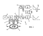
- Fig. 1 is schematically shown an inventive Device for coin recognition. These Device is usually under a standard Coin counting or coin sorting machine set up be. These machines are known. For the Understanding of Fig. 1 is only important to know that with such machines coins isolated and passed by means of transport devices to facilities which coins are to be recognized in the Location are. In the context of such machines are wrong Coins not belonging to a given type of coin belonging coins sorted out and collected separately.
- a transmitter element 1 is first recognized for electromagnetic radiation, and a receiver element 2 for electromagnetic radiation, with which according to the information submitted to it Radiation an electrical measurement signal can be generated.
- the transmitter element 1 is a light-emitting diode, which yellow or orange shines. This is particularly special good brass or bronze colored coins 4 detect.
- the receiver element 2 is a phototransistor.
- the Fig. 3 is removable, that the arrangement the transmitter element 1 and the receiver element 2 with the proviso that from the transmitter element 1 radiated electromagnetic radiation 3 on a coin 4 brought into a test position is irradiated and that the reflection radiation emitted by the coin 4 5 irradiates the receiver element 2.
- the Transmitter element 1 and the receiver element 2 are in individual aligned so that the directions of maximum Radiation intensity and maximum sensitivity each equal at an angle of 15 ° to Normals stand on a coin main surface 13.
- Evaluation unit 6 is provided by means of which Assumption of a comparison of the receiver element from the second generated and processed to an evaluation signal 12 electrical measurement signal with a predetermined comparison signal Alternatively, a "false" control signal or a "real" control signal can be generated.
- a modulated luminescent diode is irradiated, is the measuring and evaluation signal, after demodulation, wavelength selective.
- the evaluation unit 6 are the control signals in accordance with a comparison of wavelength-selective evaluation signal 12 with predetermined Wavelength-selective comparison signal bands 7 generated.
- the transmitter element 1 has a Oscillator 8 for modulation of radiated electromagnetic Radiation 3 on.
- the evaluation unit 6 comprises an AC amplifier 9 for amplification the measuring signal, preferably with filter, a detector 10 for demodulating the measurement signal, preferably a rectifier, and a DC amplifier 11 for amplifying the demodulated Signal and one in FIG. 1 for clarity half comparator not shown for comparison the demodulated evaluation signal 12 with a predetermined DC voltage range (7). in this connection it should be noted that in the embodiment shown the Output signal of the DC amplifier 11 is not immediately forms the evaluation signal 12.
- this output signal for driving a comparator used, which in turn a combination 14 from a (other and the above detector 10 on the input side parallel) detector and a sample / hold electronics controls.
- the output signal the sample / hold electronics is, if necessary after DC voltage amplification, the evaluation signal 15.
- FIG. 2 are various evaluation signals 12 and specific reference signal bands specific to a particular coin type 7 is shown.
- Fig. 2a shows the Signals for a real monocolor coin, since the Evaluation signal 12 after "catching" the sample / hold electronics lies in the comparison signal band 7.
- a downstream one Comparator shows a "real" control signal.
- the invention Device can also be bicoloured coins check as shown in Figures 2c and 2d recognizable.
- Figures 2c and 2d recognizable.
Landscapes
- Physics & Mathematics (AREA)
- General Physics & Mathematics (AREA)
- Testing Of Coins (AREA)
Description
- Fig. 1:
- eine schematische Darstellung einer erfindungsgemäßen Vorrichtung,
- Fig. 2a - 2d:
- typische Eingangssignale für einen ein "falsch"- und "echt"-Steuersignal erzeugenden Komparator und
- Fig. 3:
- eine gegenständliche Ausführungsform von Senderelement und Empfängerelement.
Claims (12)
- Vorrichtung zur Münzerkennung, mit einem Senderelement (1) für elektromagnetische Strahlung, mit einem Empfängerelement (2) für elektromagnetische Strahlung, mit welchem nach Maßgabe der darauf eingestrahlten Strahlung ein elektrisches Meßsignal erzeugbar ist, und mit einer mit dem Empfängerelement (2) verbundenen elektronischen Auswerteeinheit (6), mittels welcher nach Maßgabe eines Vergleichs des vom Empfängerelement (2) erzeugten und zu einem Auswertesignal (12) verarbeiteten elektrischen Meßsignal mit einem vorgegebenen Vergleichssignal (7) alternativ ein "falsch"-Steuersignal oder ein "echt"-Steuersignal erzeugbar ist, wobei in dem Empfängerelement (2) und der Auswerteeinheit (6) ein wellenlängenselektives Meß- und Auswertesignal (12) erzeugbar ist, und wobei mit der Auswerteeinheit (6) die Steuersignale nach Maßgabe eines Vergleichs des wellenlängenselektiven Auswertesignals (12) mit vorgegebenen wellenlängenselektiven Vergleichssignalbändern (7) erzeugbar sind.
dadurch gekennzeichnet, daß die Anordnung des Senderelements (1) und des Empfängerelements (2) mit der Maßgabe getroffen ist, daß von dem Senderelement (1) abgestrahlte elektromagnetische Strahlung (3) auf eine in eine Prüfposition gebrachte Münze (4) einstrahlt und daß zumindest ein Teil einer von der Münze (4) abgestrahlten Reflektionsstrahlung (5) aus der eingestrahlten elektromagnetischen Strahlung (3) auf das Empfängerelement (2) einstrahlt, und
daß das Senderelement (1) und das Empfängerelement (2) so ausgerichtet sind, daß die Richtungen maximaler Strahlungsintensität sowie maximaler Empfindlichkeit jeweils gleich oder verschieden in einem Winkel von 0 - 50° zur Normalen auf einer Münzenhauptfläche (13) stehen. - Vorrichtung nach Anspruch 1, dadurch gekennzeichnet, daß mit dem Senderelement (1) elektromagnetische Strahlung wellenlängenselektiv abstrahlbar und/oder mit dem Empfängerelement (2) elektromagnetische Strahlung wellenlängenselektiv aufnehmbar ist.
- Vorrichtung nach Anspruch 1 oder 2, dadurch gekennzeichnet, daß das Senderelement (1) eine Lumineszenzdiode aufweist.
- Vorrichtung nach einem der Ansprüche 1 bis 3, dadurch gekennzeichnet, daß das Senderelement (1) mehrere wellenlängenselektiv abstrahlende Sendereinheiten aufweist, wobei die Strahlungsspektren der Sendereinheiten nichtüberlappend sind und daß im Empfängerelement (2) getrennte, jeweils einer Sendereinheit zuordbare Meßsignale erzeugbar sind.
- Vorrichtung nach einem der Ansprüche 1 bis 4, dadurch gekennzeichnet, daß das Senderelement (1) zwei Lumineszenzdioden mit unterschiedlichen Bandlücken aufweist.
- Vorrichtung nach einem der Ansprüche 1 bis 5, dadurch gekennzeichnet, daß das Senderelement (1) zur Abstrahlung modulierter elektromagnetischer Wellen eingerichtet ist.
- Vorrichtung nach einem der Ansprüche 1 bis 6, dadurch gekennzeichnet, daß das Empfängerelement (2) einen Photowiderstand, eine pn-Photodiode, eine pin-Photodiode, eine Avalanche-Photodiode oder einen Phototransistor aufweist.
- Vorrichtung nach einem der Ansprüche 1 bis 7, dadurch gekennzeichnet, daß das Senderelement (1) und das Empfängerelement (2) so ausgerichtet sind, daß die Richtungen maximaler Strahlungsintensität sowie maximaler Empfindlichkeit jeweils gleich oder verschieden in einem Winkel von 5 - 30°, vorzugsweise 14 - 16°, zur Normalen auf einer Münzenhauptfläche (13) stehen.
- Vorrichtung nach einem der Ansprüche 1 bis 8, dadurch gekennzeichnet, daß das Senderelement (1) einen Oszillator (8) zur Modulation der abgestrahlten elektromagnetischen Strahlung (3) aufweist, und daß die Auswerteeinheit (6) einen Wechselspannungsverstärker (9) zur Verstärkung des Meßsignals, vorzugsweise mit Filter, einen Detektor (10) zur Demodulation des Meßsignals, vorzugsweise einen Gleichrichter, und einen Gleichspannungsverstärker (11) zur Verstärkung des demodulierten Signals und einen Komparator zum Vergleich des demodulierten Auswertesignals (12) mit einem vorgegebenen Gleichspannungsbereich (7) aufweist.
- Verfahren zur Prüfung von Münzen (4), wobei mit einem Senderelement (1) elektromagnetische Strahlung (3) auf eine Münze eingestrahlt wird, wobei die eingestrahlte elektromagnetische Strahlung (3) von der Oberfläche der Münze (4) reflektiert wird und wobei die reflektierte elektromagnetische Strahlung (5) mit einem Empfängerelement (2) aufgefangen und in ein elektrisches Meßsignal umgewandelt wird, wobei das Meßsignal einer Auswerteeinheit (6) zugeführt und mit einem vorgegebenen Vergleichssignal verglichen wird, und wobei nach Maßgabe des Ergebnisses des Vergleichs alternativ ein "falsch"-Steuersignal oder ein "echt"-Steuersignal erzeugt wird, wobei in der Auswerteeinheit (6) ein wellenlängenselektives Auswertesignal (12) erzeugt und mit wellenlängenselektiven Vergleichsignalbändern (7) verglichen wird,
dadurch gekennzeichnet, daß das Senderelement (1) und das Empfängerelement (2) so ausgerichtet werden, daß die Richtungen maximaler Strahlungsintensität sowie maximaler Empfindlichkeit jeweils gleich oder verschieden in einem Winkel von 0 - 50° zur Normalen auf einer Münzenhauptfläche (13) stehen. - Verfahren nach Anspruch 10, dadurch gekennzeichnet, daß die Linienbreite der elektromagnetischen Strahlung weniger als 0,4, vorzugsweise weniger als 0,1, höchstvorzugsweise weniger als 0,07, beträgt.
- Verfahren nach Anspruch 10 oder 11, dadurch gekennzeichnet, daß eine Vorrichtung nach einem der Ansprüche 1 bis 9 verwendet wird.
Applications Claiming Priority (2)
| Application Number | Priority Date | Filing Date | Title |
|---|---|---|---|
| DE19909851 | 1999-03-08 | ||
| DE19909851A DE19909851C2 (de) | 1999-03-08 | 1999-03-08 | Vorrichtung zur Unterscheidung falscher von echten Münzen |
Publications (2)
| Publication Number | Publication Date |
|---|---|
| EP1035519A1 EP1035519A1 (de) | 2000-09-13 |
| EP1035519B1 true EP1035519B1 (de) | 2005-08-31 |
Family
ID=7899907
Family Applications (1)
| Application Number | Title | Priority Date | Filing Date |
|---|---|---|---|
| EP00250044A Expired - Lifetime EP1035519B1 (de) | 1999-03-08 | 2000-02-10 | Vorrichtung zur Münzerkennung |
Country Status (5)
| Country | Link |
|---|---|
| US (1) | US6417471B1 (de) |
| EP (1) | EP1035519B1 (de) |
| AT (1) | ATE303637T1 (de) |
| AU (1) | AU762905B2 (de) |
| DE (2) | DE19909851C2 (de) |
Families Citing this family (9)
| Publication number | Priority date | Publication date | Assignee | Title |
|---|---|---|---|---|
| SE520847C2 (sv) * | 1999-02-10 | 2003-09-02 | Scan Coin Ind Ab | Myntsärskiljande anordning, mynthanteringsapparat inbegripande en sådan anordning samt en metod för särskiljning av mynt |
| US6736250B2 (en) * | 2001-09-28 | 2004-05-18 | Harold E. Mattice | Method and apparatus for fraud detection |
| DE10222771A1 (de) * | 2002-05-16 | 2003-12-04 | Walter Hanke Mech Werkstaetten | Verfahren und optische Meßeinrichtung zum Prüfen von Münzen oder münzähnlichen Gegenständen |
| DE10300608B4 (de) * | 2003-01-10 | 2004-09-30 | National Rejectors, Inc. Gmbh | Verfahren zur Erkennung eines Prägebildes einer Münze in einem Münzautomaten |
| US20070007723A1 (en) * | 2005-02-28 | 2007-01-11 | Aruze Corp. | Gaming machine and coin selection device |
| DE102009020487A1 (de) | 2009-05-08 | 2010-11-11 | Bundesrepublik Deutschland, vertr.d.d. Bundesministerium für Wirtschaft und Technologie, d.vertr.d.d. Präsidenten der Physikalisch-Technischen Bundesanstalt | Vorrichtung und Verfahren zur Erkennung einer Münze |
| US8661889B2 (en) * | 2009-07-16 | 2014-03-04 | Duane C. Blake | AURA devices and methods for increasing rare coin value |
| DE102012014958A1 (de) * | 2012-07-30 | 2014-02-13 | Crane Payment Solutions Gmbh | Münze und Verfahren zum Prüfen der Münze |
| TWI675353B (zh) * | 2018-06-08 | 2019-10-21 | 慶餘科技股份有限公司 | 自動辨識硬幣真偽的系統及其操作方法 |
Citations (1)
| Publication number | Priority date | Publication date | Assignee | Title |
|---|---|---|---|---|
| JPH0546840A (ja) * | 1991-08-07 | 1993-02-26 | Glory Ltd | 硬貨識別装置 |
Family Cites Families (13)
| Publication number | Priority date | Publication date | Assignee | Title |
|---|---|---|---|---|
| BE748076A (fr) * | 1969-03-31 | 1970-09-28 | F A T M E Fabbrica Apparecchia | Analyseur electronique de pieces de monnaie metalliques |
| GB1397083A (en) * | 1971-05-24 | 1975-06-11 | Mars Inc | Coin selector utilizing inductive sensors |
| CH558962A (de) * | 1973-06-01 | 1975-02-14 | Landis & Gyr Ag | Vorrichtung zum vergleich der spektralen remission oder transmission eines prueflings und eines standards. |
| US4333557A (en) * | 1980-02-21 | 1982-06-08 | Kozak George M | Solid state slug rejector |
| GB2078368B (en) * | 1980-06-20 | 1984-03-14 | De La Rue Syst | Sorting objects by colour |
| FR2515395B1 (fr) * | 1981-10-27 | 1985-05-31 | Doucet Joel | Selecteur multipiece de monnaie |
| JP2567654B2 (ja) * | 1988-03-31 | 1996-12-25 | 株式会社 日本コンラックス | 硬貨選別方法および装置 |
| US5046841A (en) * | 1989-01-19 | 1991-09-10 | Idx, Inc. | Token having a predetermined optical characteristic, and a token validation device for use therewith |
| CH683463A5 (de) * | 1991-12-10 | 1994-03-15 | Ascom Autelca Ag | Verfahren zum Prüfen einer Münze. |
| CH684222A5 (de) * | 1992-03-10 | 1994-07-29 | Mars Inc | Einrichtung zur Klassifizierung eines Musters, insbesondere von einer Banknote oder von einer Münze. |
| JP3525360B2 (ja) * | 1994-05-19 | 2004-05-10 | ローレルバンクマシン株式会社 | 硬貨判別装置 |
| DE19507482A1 (de) * | 1995-03-03 | 1996-09-05 | Herbert Weiss | Verfahren zum Sortieren von Münzen |
| US6142285A (en) * | 1996-05-21 | 2000-11-07 | Digitall Inc | Coin testing apparatus and method |
-
1999
- 1999-03-08 DE DE19909851A patent/DE19909851C2/de not_active Expired - Fee Related
-
2000
- 2000-02-10 AT AT00250044T patent/ATE303637T1/de not_active IP Right Cessation
- 2000-02-10 EP EP00250044A patent/EP1035519B1/de not_active Expired - Lifetime
- 2000-02-10 DE DE50011044T patent/DE50011044D1/de not_active Expired - Fee Related
- 2000-02-23 AU AU19423/00A patent/AU762905B2/en not_active Ceased
- 2000-03-07 US US09/520,863 patent/US6417471B1/en not_active Expired - Fee Related
Patent Citations (1)
| Publication number | Priority date | Publication date | Assignee | Title |
|---|---|---|---|---|
| JPH0546840A (ja) * | 1991-08-07 | 1993-02-26 | Glory Ltd | 硬貨識別装置 |
Also Published As
| Publication number | Publication date |
|---|---|
| US6417471B1 (en) | 2002-07-09 |
| DE50011044D1 (de) | 2005-10-06 |
| AU762905B2 (en) | 2003-07-10 |
| DE19909851A1 (de) | 2000-09-21 |
| ATE303637T1 (de) | 2005-09-15 |
| DE19909851C2 (de) | 2003-09-04 |
| EP1035519A1 (de) | 2000-09-13 |
| AU1942300A (en) | 2000-09-14 |
Similar Documents
| Publication | Publication Date | Title |
|---|---|---|
| DE60112890T3 (de) | Verfahren zur überwachung von dokumenten | |
| DE69418596T2 (de) | Erfassung von verfälschten objekten | |
| DE3784142T2 (de) | Pruefung eines artikels. | |
| DE69515445T2 (de) | Verfahren und Vorrichtung zum Kennzeichnen und Unterscheiden von Banknoten und legalen Zahlungsmitteln | |
| EP1245007B1 (de) | Vorrichtung und verfahren zur echtheitsprüfung von banknoten | |
| DE69910550T2 (de) | Verfahren und vorrichtung zur überwachung von artikeln | |
| DE2320731B2 (de) | Faelschungsgesichertes wertpapier | |
| EP1112555B1 (de) | Verfahren und Vorrichtung zur Zustandsprüfung von Wertpapieren mittels einer Dunkelfeldmessung als auch einer Hellfeldmessung. | |
| DE69907468T2 (de) | System zur farbklassifizierung von fasern | |
| DE10212734B4 (de) | Verfahren und Vorrichtung zur Identifikation und Authentifikation eines Gegenstandes | |
| EP1035519A1 (de) | Vorrichtung zur Münzerkennung | |
| EP1547026B1 (de) | Vorrichtung und verfahren zur prüfung der authentizität einer fälschungssicheren markierung | |
| EP2377104A1 (de) | Vorrichtung und verfahren zum nachweis von reflektiertem und/oder emittiertem licht eines gegenstandes | |
| WO2019243199A1 (de) | Vorrichtung und verfahren zur erkennung und/oder bewertung von erzeugnissen oder produkten | |
| EP3400584A1 (de) | Vollständigkeitsprüfung eines wertdokuments | |
| EP2160269A1 (de) | Werkzeugmaschinenüberwachungsvorrichtung | |
| EP1265198A2 (de) | Vorrichtung und Verfahren zur Untersuchung von Dokumenten | |
| EP3616171B1 (de) | Verfahren zum identifizieren von pfandgut | |
| DE3720388C2 (de) | ||
| DE19701513C2 (de) | Prüfverfahren und Prüfeinrichtung für Echtheitskontrolle von Echtheitsmarken | |
| DE19718916A1 (de) | Anwendung und Verfahren zur Prüfung von Kokumenten mit beugungsoptisch wirksamen Sicherheitsschichten | |
| WO1999032875A1 (de) | Verfahren und vorrichtung zur bestimmung der farbe von in waschmaschinen zu behandelnden gütern | |
| WO2006018191A1 (de) | Verfahren und vorrichtung zum messen von blattgut | |
| DE102017129986A1 (de) | Vorrichtung für ein portables Smart-Gerät und Verfahren zur Produktprüfung | |
| DE3900056A1 (de) | Identifizierungsvorrichtung mit optisch lesbaren etiketten und hierfuer geeignete etiketten |
Legal Events
| Date | Code | Title | Description |
|---|---|---|---|
| PUAI | Public reference made under article 153(3) epc to a published international application that has entered the european phase |
Free format text: ORIGINAL CODE: 0009012 |
|
| AK | Designated contracting states |
Kind code of ref document: A1 Designated state(s): AT BE CH CY DE DK ES FI FR GB GR IE IT LI LU MC NL PT SE |
|
| AX | Request for extension of the european patent |
Free format text: AL;LT;LV;MK;RO;SI |
|
| 17P | Request for examination filed |
Effective date: 20010222 |
|
| AKX | Designation fees paid |
Free format text: AT BE CH CY DE DK ES FI FR GB GR IE IT LI LU MC NL PT SE |
|
| AXX | Extension fees paid |
Free format text: AL PAYMENT 20010222;LT PAYMENT 20010222;LV PAYMENT 20010222;MK PAYMENT 20010222;RO PAYMENT 20010222;SI PAYMENT 20010222 |
|
| 17Q | First examination report despatched |
Effective date: 20030829 |
|
| RAP1 | Party data changed (applicant data changed or rights of an application transferred) |
Owner name: SCAN COIN INDUSTRIES AB |
|
| GRAP | Despatch of communication of intention to grant a patent |
Free format text: ORIGINAL CODE: EPIDOSNIGR1 |
|
| GRAS | Grant fee paid |
Free format text: ORIGINAL CODE: EPIDOSNIGR3 |
|
| GRAA | (expected) grant |
Free format text: ORIGINAL CODE: 0009210 |
|
| AK | Designated contracting states |
Kind code of ref document: B1 Designated state(s): AT BE CH CY DE DK ES FI FR GB GR IE IT LI LU MC NL PT SE |
|
| AX | Request for extension of the european patent |
Extension state: AL LT LV MK RO SI |
|
| PG25 | Lapsed in a contracting state [announced via postgrant information from national office to epo] |
Ref country code: FI Free format text: LAPSE BECAUSE OF FAILURE TO SUBMIT A TRANSLATION OF THE DESCRIPTION OR TO PAY THE FEE WITHIN THE PRESCRIBED TIME-LIMIT Effective date: 20050831 Ref country code: IE Free format text: LAPSE BECAUSE OF FAILURE TO SUBMIT A TRANSLATION OF THE DESCRIPTION OR TO PAY THE FEE WITHIN THE PRESCRIBED TIME-LIMIT Effective date: 20050831 |
|
| REG | Reference to a national code |
Ref country code: CH Ref legal event code: EP Ref country code: GB Ref legal event code: FG4D Free format text: NOT ENGLISH |
|
| REG | Reference to a national code |
Ref country code: IE Ref legal event code: FG4D Free format text: LANGUAGE OF EP DOCUMENT: GERMAN |
|
| REF | Corresponds to: |
Ref document number: 50011044 Country of ref document: DE Date of ref document: 20051006 Kind code of ref document: P |
|
| PG25 | Lapsed in a contracting state [announced via postgrant information from national office to epo] |
Ref country code: DK Free format text: LAPSE BECAUSE OF FAILURE TO SUBMIT A TRANSLATION OF THE DESCRIPTION OR TO PAY THE FEE WITHIN THE PRESCRIBED TIME-LIMIT Effective date: 20051130 Ref country code: GR Free format text: LAPSE BECAUSE OF FAILURE TO SUBMIT A TRANSLATION OF THE DESCRIPTION OR TO PAY THE FEE WITHIN THE PRESCRIBED TIME-LIMIT Effective date: 20051130 |
|
| GBT | Gb: translation of ep patent filed (gb section 77(6)(a)/1977) |
Effective date: 20051115 |
|
| PG25 | Lapsed in a contracting state [announced via postgrant information from national office to epo] |
Ref country code: ES Free format text: LAPSE BECAUSE OF FAILURE TO SUBMIT A TRANSLATION OF THE DESCRIPTION OR TO PAY THE FEE WITHIN THE PRESCRIBED TIME-LIMIT Effective date: 20051212 |
|
| REG | Reference to a national code |
Ref country code: SE Ref legal event code: TRGR |
|
| PG25 | Lapsed in a contracting state [announced via postgrant information from national office to epo] |
Ref country code: AT Free format text: LAPSE BECAUSE OF NON-PAYMENT OF DUE FEES Effective date: 20060210 |
|
| PG25 | Lapsed in a contracting state [announced via postgrant information from national office to epo] |
Ref country code: PT Free format text: LAPSE BECAUSE OF FAILURE TO SUBMIT A TRANSLATION OF THE DESCRIPTION OR TO PAY THE FEE WITHIN THE PRESCRIBED TIME-LIMIT Effective date: 20060222 |
|
| LTIE | Lt: invalidation of european patent or patent extension |
Effective date: 20050831 |
|
| PG25 | Lapsed in a contracting state [announced via postgrant information from national office to epo] |
Ref country code: LI Free format text: LAPSE BECAUSE OF NON-PAYMENT OF DUE FEES Effective date: 20060228 Ref country code: MC Free format text: LAPSE BECAUSE OF NON-PAYMENT OF DUE FEES Effective date: 20060228 Ref country code: BE Free format text: LAPSE BECAUSE OF NON-PAYMENT OF DUE FEES Effective date: 20060228 Ref country code: LU Free format text: LAPSE BECAUSE OF NON-PAYMENT OF DUE FEES Effective date: 20060228 Ref country code: CH Free format text: LAPSE BECAUSE OF NON-PAYMENT OF DUE FEES Effective date: 20060228 |
|
| REG | Reference to a national code |
Ref country code: IE Ref legal event code: FD4D |
|
| ET | Fr: translation filed | ||
| PLBE | No opposition filed within time limit |
Free format text: ORIGINAL CODE: 0009261 |
|
| 26N | No opposition filed |
Effective date: 20060601 |
|
| REG | Reference to a national code |
Ref country code: CH Ref legal event code: PL |
|
| BERE | Be: lapsed |
Owner name: SCAN COIN INDUSTRIES A.B. Effective date: 20060228 |
|
| PGFP | Annual fee paid to national office [announced via postgrant information from national office to epo] |
Ref country code: DE Payment date: 20080129 Year of fee payment: 9 Ref country code: GB Payment date: 20080222 Year of fee payment: 9 Ref country code: IT Payment date: 20080227 Year of fee payment: 9 Ref country code: NL Payment date: 20080220 Year of fee payment: 9 Ref country code: SE Payment date: 20080225 Year of fee payment: 9 |
|
| PGFP | Annual fee paid to national office [announced via postgrant information from national office to epo] |
Ref country code: FR Payment date: 20080219 Year of fee payment: 9 |
|
| PG25 | Lapsed in a contracting state [announced via postgrant information from national office to epo] |
Ref country code: CY Free format text: LAPSE BECAUSE OF FAILURE TO SUBMIT A TRANSLATION OF THE DESCRIPTION OR TO PAY THE FEE WITHIN THE PRESCRIBED TIME-LIMIT Effective date: 20050831 |
|
| EUG | Se: european patent has lapsed | ||
| GBPC | Gb: european patent ceased through non-payment of renewal fee |
Effective date: 20090210 |
|
| NLV4 | Nl: lapsed or anulled due to non-payment of the annual fee |
Effective date: 20090901 |
|
| REG | Reference to a national code |
Ref country code: FR Ref legal event code: ST Effective date: 20091030 |
|
| PG25 | Lapsed in a contracting state [announced via postgrant information from national office to epo] |
Ref country code: NL Free format text: LAPSE BECAUSE OF NON-PAYMENT OF DUE FEES Effective date: 20090901 |
|
| PG25 | Lapsed in a contracting state [announced via postgrant information from national office to epo] |
Ref country code: DE Free format text: LAPSE BECAUSE OF NON-PAYMENT OF DUE FEES Effective date: 20090901 |
|
| PG25 | Lapsed in a contracting state [announced via postgrant information from national office to epo] |
Ref country code: GB Free format text: LAPSE BECAUSE OF NON-PAYMENT OF DUE FEES Effective date: 20090210 Ref country code: FR Free format text: LAPSE BECAUSE OF NON-PAYMENT OF DUE FEES Effective date: 20090302 |
|
| PG25 | Lapsed in a contracting state [announced via postgrant information from national office to epo] |
Ref country code: IT Free format text: LAPSE BECAUSE OF NON-PAYMENT OF DUE FEES Effective date: 20090210 |
|
| PG25 | Lapsed in a contracting state [announced via postgrant information from national office to epo] |
Ref country code: SE Free format text: LAPSE BECAUSE OF NON-PAYMENT OF DUE FEES Effective date: 20090211 |