EP1036411B1 - Fabrication d'un semiconducteur de puissance - Google Patents
Fabrication d'un semiconducteur de puissance Download PDFInfo
- Publication number
- EP1036411B1 EP1036411B1 EP99932833A EP99932833A EP1036411B1 EP 1036411 B1 EP1036411 B1 EP 1036411B1 EP 99932833 A EP99932833 A EP 99932833A EP 99932833 A EP99932833 A EP 99932833A EP 1036411 B1 EP1036411 B1 EP 1036411B1
- Authority
- EP
- European Patent Office
- Prior art keywords
- doped
- region
- gate
- sidewall extension
- conductivity type
- Prior art date
- Legal status (The legal status is an assumption and is not a legal conclusion. Google has not performed a legal analysis and makes no representation as to the accuracy of the status listed.)
- Expired - Lifetime
Links
Images
Classifications
-
- H—ELECTRICITY
- H10—SEMICONDUCTOR DEVICES; ELECTRIC SOLID-STATE DEVICES NOT OTHERWISE PROVIDED FOR
- H10D—INORGANIC ELECTRIC SEMICONDUCTOR DEVICES
- H10D30/00—Field-effect transistors [FET]
- H10D30/60—Insulated-gate field-effect transistors [IGFET]
- H10D30/64—Double-diffused metal-oxide semiconductor [DMOS] FETs
- H10D30/66—Vertical DMOS [VDMOS] FETs
- H10D30/668—Vertical DMOS [VDMOS] FETs having trench gate electrodes, e.g. UMOS transistors
-
- H—ELECTRICITY
- H10—SEMICONDUCTOR DEVICES; ELECTRIC SOLID-STATE DEVICES NOT OTHERWISE PROVIDED FOR
- H10P—GENERIC PROCESSES OR APPARATUS FOR THE MANUFACTURE OR TREATMENT OF DEVICES COVERED BY CLASS H10
- H10P10/00—Bonding of wafers, substrates or parts of devices
-
- H—ELECTRICITY
- H10—SEMICONDUCTOR DEVICES; ELECTRIC SOLID-STATE DEVICES NOT OTHERWISE PROVIDED FOR
- H10D—INORGANIC ELECTRIC SEMICONDUCTOR DEVICES
- H10D12/00—Bipolar devices controlled by the field effect, e.g. insulated-gate bipolar transistors [IGBT]
- H10D12/01—Manufacture or treatment
- H10D12/031—Manufacture or treatment of IGBTs
- H10D12/032—Manufacture or treatment of IGBTs of vertical IGBTs
- H10D12/038—Manufacture or treatment of IGBTs of vertical IGBTs having a recessed gate, e.g. trench-gate IGBTs
-
- H—ELECTRICITY
- H10—SEMICONDUCTOR DEVICES; ELECTRIC SOLID-STATE DEVICES NOT OTHERWISE PROVIDED FOR
- H10D—INORGANIC ELECTRIC SEMICONDUCTOR DEVICES
- H10D62/00—Semiconductor bodies, or regions thereof, of devices having potential barriers
- H10D62/10—Shapes, relative sizes or dispositions of the regions of the semiconductor bodies; Shapes of the semiconductor bodies
- H10D62/13—Semiconductor regions connected to electrodes carrying current to be rectified, amplified or switched, e.g. source or drain regions
- H10D62/149—Source or drain regions of field-effect devices
- H10D62/151—Source or drain regions of field-effect devices of IGFETs
- H10D62/152—Source regions of DMOS transistors
- H10D62/155—Shapes
-
- H—ELECTRICITY
- H10—SEMICONDUCTOR DEVICES; ELECTRIC SOLID-STATE DEVICES NOT OTHERWISE PROVIDED FOR
- H10D—INORGANIC ELECTRIC SEMICONDUCTOR DEVICES
- H10D62/00—Semiconductor bodies, or regions thereof, of devices having potential barriers
- H10D62/10—Shapes, relative sizes or dispositions of the regions of the semiconductor bodies; Shapes of the semiconductor bodies
- H10D62/17—Semiconductor regions connected to electrodes not carrying current to be rectified, amplified or switched, e.g. channel regions
- H10D62/393—Body regions of DMOS transistors or IGBTs
-
- H—ELECTRICITY
- H10—SEMICONDUCTOR DEVICES; ELECTRIC SOLID-STATE DEVICES NOT OTHERWISE PROVIDED FOR
- H10D—INORGANIC ELECTRIC SEMICONDUCTOR DEVICES
- H10D64/00—Electrodes of devices having potential barriers
- H10D64/20—Electrodes characterised by their shapes, relative sizes or dispositions
- H10D64/27—Electrodes not carrying the current to be rectified, amplified, oscillated or switched, e.g. gates
- H10D64/311—Gate electrodes for field-effect devices
- H10D64/411—Gate electrodes for field-effect devices for FETs
- H10D64/511—Gate electrodes for field-effect devices for FETs for IGFETs
- H10D64/512—Disposition of the gate electrodes, e.g. buried gates
- H10D64/513—Disposition of the gate electrodes, e.g. buried gates within recesses in the substrate, e.g. trench gates, groove gates or buried gates
-
- H—ELECTRICITY
- H10—SEMICONDUCTOR DEVICES; ELECTRIC SOLID-STATE DEVICES NOT OTHERWISE PROVIDED FOR
- H10P—GENERIC PROCESSES OR APPARATUS FOR THE MANUFACTURE OR TREATMENT OF DEVICES COVERED BY CLASS H10
- H10P32/00—Diffusion of dopants within, into or out of wafers, substrates or parts of devices
- H10P32/10—Diffusion of dopants within, into or out of semiconductor bodies or layers
- H10P32/14—Diffusion of dopants within, into or out of semiconductor bodies or layers within a single semiconductor body or layer in a solid phase; between different semiconductor bodies or layers, both in a solid phase
- H10P32/1408—Diffusion of dopants within, into or out of semiconductor bodies or layers within a single semiconductor body or layer in a solid phase; between different semiconductor bodies or layers, both in a solid phase from or through or into an external applied layer, e.g. photoresist or nitride layers
- H10P32/1414—Diffusion of dopants within, into or out of semiconductor bodies or layers within a single semiconductor body or layer in a solid phase; between different semiconductor bodies or layers, both in a solid phase from or through or into an external applied layer, e.g. photoresist or nitride layers the applied layer being silicon, silicide or SIPOS, e.g. polysilicon or porous silicon
-
- H—ELECTRICITY
- H10—SEMICONDUCTOR DEVICES; ELECTRIC SOLID-STATE DEVICES NOT OTHERWISE PROVIDED FOR
- H10P—GENERIC PROCESSES OR APPARATUS FOR THE MANUFACTURE OR TREATMENT OF DEVICES COVERED BY CLASS H10
- H10P32/00—Diffusion of dopants within, into or out of wafers, substrates or parts of devices
- H10P32/10—Diffusion of dopants within, into or out of semiconductor bodies or layers
- H10P32/17—Diffusion of dopants within, into or out of semiconductor bodies or layers characterised by the semiconductor material
- H10P32/171—Diffusion of dopants within, into or out of semiconductor bodies or layers characterised by the semiconductor material being group IV material
Definitions
- This invention relates to methods of manufacturing a semiconductor power device having a source region formed using a sidewall extension of an upstanding gate structure, particularly, but not exclusively, comprising a trench-gate.
- the device may be, for example, an insulated-gate field-effect power transistor (hereinafter termed MOSFET) or an insulated-gate bipolar transistor (hereinafter termed IGBT).
- MOSFET insulated-gate field-effect power transistor
- IGBT insulated-gate bipolar transistor
- an upstanding gate structure is formed at a major surface of a semiconductor body, and a sidewall extension (also termed a "spacer") is provided at upstanding sides of the gate structure to form a step with an adjacent surface area of a body region of a first conductivity type.
- the body region of the first conductivity type extends adjacent to the gate structure to provide the device with a channel-accommodating portion, to which the gate is capacitively coupled.
- the sidewall extension comprises doped semiconductor material of opposite, second conductivity type which is separated from the gate by insulating material and which provides a source region of the device.
- the channel-accommodating portion forms a p-n junction with the source region.
- a source electrode is deposited over the step so as to contact the doped semiconductor material of the sidewall extension and the adjacent surface area of the first conductivity type.
- the source region is self-aligned with the trench-gate, by means of the spacers.
- the initially-formed spacer is an etchant mask on part of a surface region of the second conductivity type in the body, and exposed areas of the surface region are then etched away to leave a remaining portion of the second conductivity type under the mask as the source region.
- the spacer is of doped material (for example, doped polycrystalline silicon, or a doped oxide or glass) and serves as a dopant diffusion source for diffusing the dopant of the second conductivity type into the semiconductor body to form the source region.
- United States patent specification US-A-5,665,619 discloses a different trench-gate device process in which a spacer (sidewall extension) of insulating material (undoped oxide) is provided on part of a previously-formed source region so as to define a contact window that is self-aligned to the upstanding insulated trench-gate structure.
- a high-doped portion is then formed in the body by a blanket implant of dopant of the first conductivity type.
- This high-doped portion has a doping concentration of said first conductivity type which is higher than that of the channel-accommodating portion but lower than the conductivity-determining dopant concentration of the source region.
- the source region overdopes the ends of the high-doped portion which extends to a shallower depth in the body than the p-n junction between the source region and the channel-accommodating portion of the body region.
- the source electrode contacts the high-doped portion of the body region of the first conductivity type and the adjacent surface area of the source region of the second conductivity type. No such separately-provided high-doped portion of the body region is described in the devices disclosed in US-A-5,378,655.
- the sidewall extension (comprising the doped semiconductor material of the source region) is used to mask the underlying area of the body where the channel is accommodated.
- the channel-accommodating portion is protected in this way from the high doping concentration of the localised high-doped portion, so that the channel threshold voltage of the device is not adversely affected.
- Such a self-aligned process in accordance with the invention readily permits the localised high-doped portion of the first conductivity type to be provided to a greater depth in the semiconductor body than the p-n junction between the source region and the channel-accommodating portion of the body region.
- This arrangement improves the current flow from deep in the body region to the source electrode.
- the source electrode provides an efficient ohmic contact to the body region, and parasitic bipolar transistor action in the device is reduced, so improving the ruggedness of the device.
- the greater depth relationship between the said localised high-doped portion and said p-n junction is achieved by means of the step-up and step-down associated with the source region which comprises the doped semiconductor material of the sidewall extension at the upstanding sides of the gate structure.
- the localised high-doped portion of the body region is formed by introducing dopant via the surface area adjacent to the bottom of the step, while using this step (the sidewall extension) as a mask that comprises the doped semiconductor material for the source region.
- the depth of the locally-provided high-doped portion in the semiconductor body is determined with respect to this adjacent surface area at the step-down level, whereas the thickness of the source region is determined with respect to the step-up level of the doped semiconductor material of the sidewall extension.
- the method permits the realisation of an even greater depth for the localised high-doped portion of the body region.
- the localised high-doped portion may be provided to a greater depth in the semiconductor body than the channel-accommodating portion or even to a greater depth in the semiconductor body than the bottom of a trench-gate, for example.
- the breakdown voltage of the device permits the breakdown voltage of the device to be determined by avalanche breakdown of a deep p-n junction between this deep localised high-doped portion and the underlying body portion of the second conductivity type, rather than by avalanche breakdown of a p-n junction between the shallow body region and the underlying body portion or by breakdown at a bottom corner of the trench as may otherwise occur with some trench-gate device designs.
- Figure 10 illustrates an exemplary embodiment of a cellular power semiconductor device having a trench-gate 11.
- a channel-accommodating portion 15a of a body region 15 of a first conductivity type i.e. p-type in this example
- the gate 11 is present in a trench 20 which extends through the regions 13 and 15 into an underlying portion of the drain region 14.
- the application of a voltage signal to the gate 11 in the on-state of the device serves in known manner for inducing a conduction channel 12 in the region portion 15a and for controlling current flow in this conduction channel 12 between the source and drain regions 13 and 14.
- the source region 13 is located adjacent to the top major surface 10a of the device body and is contacted by a source electrode 33.
- Figure 10 shows a vertical device structure in which the region 14 may be a drain-drift region formed by an epitaxial layer of high resistivity on a substrate region 14a of high conductivity.
- This substrate region 14a may be of the same conductivity type (n-type in this example) as the region 14 to provide a vertical MOSFET, or it may be of opposite conductivity type (p-type in this example) to provide a vertical IGBT.
- the substrate region 14a is contacted at the bottom major surface 10b of the device body by an electrode 34, called the drain electrode in the case of a MOSFET and called the anode electrode in the case of an IGBT.
- the device body is of monocrystalline silicon
- the gate 11 is typically of conductive polycrystalline silicon.
- the device of Figure 10 is manufactured by a method which, in overview, includes the following steps:
- This high-doped portion 15b of the body region 15 that is contacted by the source electrode 33 at the said adjacent surface area 10a'.
- This high-doped portion 15b has a doping concentration (P+) of the first conductivity type which is higher than that (P) of the channel-accommodating portion 15a but lower than the conductivity-determining dopant concentration (N++) of the doped semiconductor material 13a of the sidewall extension 30 that provides the source region 13.
- the high-doped portion 15b is provided to a greater depth in the semiconductor body 10 than the p-n junction 18 between the source region 13 and the channel-accommodating portion 15a of the body region 15, and is preferably even deeper (as illustrated in Figures 7 to 10) than the p-n junction 19a between the channel-accommodating portion 15a and the underlying drain region 14.
- the doping concentration (P+) of the high-doped portion 15b may be, for example, 10 18 to 10 19 boron atoms cm -3
- that (P) of the channel-accommodating portion 15a may be, for example, 10 16 to 10 17 boron atoms cm -3
- the conductivity-determining dopant concentration (N++) of the doped semiconductor material 13a of the sidewall extension 30 may be, for example, 10 20 to 10 22 phosphorus or arsenic atoms cm -3 .
- the depth (below the surface area 10a') of the high-doped portion 15b may be, for example, 1.5 ⁇ m to 3 ⁇ m (micrometres), whereas those of the source p-n junction 18 and drain p-n junction 19a with the channel-accommodating portion 15a may be, for example, 0.1 ⁇ m to 0.6 ⁇ m and 1 ⁇ m to 2 ⁇ m, respectively.
- the depth of the trench 20 may be, for example, 1.5 ⁇ m to 3 ⁇ m.
- the bulk of the source region 13 in the device of Figure 10 is of doped polycrystalline silicon material 13a deposited on the body surface 10a ( Figure 6).
- the height of the doped sidewall extension 30 (source region material 13a) which is retained above the surface 10a may be, for example, 0.5 ⁇ m to 1.5 ⁇ m
- This arrangement permits the realisation of a device with a very shallow depth for the p-n junction 18 between the source region 13 and the channel-accommodating portion 15a, while using doped semiconductor material 13a of high conductivity in the step so as to avoid a high resistance in this shallow source region 13.
- the device can be made with a short channel length 12 and so with a low on-resistance between the source and drain regions 13 and 14.
- the breakdown voltage of the device can be determined by avalanche breakdown of the deep p-n junction 19b between the deep localised high-doped portion 15b and the underlying region 14, rather than by avalanche breakdown of the shallower p-n junction 15a formed by the channel-accommodating portion 15a.
- FIG. 10 No plan view of the cellular layout geometry is shown in the drawings, because the method of Figures 1 to 10 may be used for quite different, known cell geometries.
- the cells may have a square geometry as illustrated in Figure 14 of US-A-5,378,655, or they may have a close-packed hexagonal geometry or an elongate stripe geometry.
- the trench 20 (with its gate 11) extends around the boundary of each cell.
- Figure 10 shows only a few cells, but typically the device comprises many thousands of these parallel cells between the electrodes 33 and 34.
- the active cellular area of the device may be bounded around the periphery of the body 10 by various known peripheral termination schemes (also not shown).
- Such schemes normally include the formation of a thick field-oxide layer at the peripheral area of the body surface 10a, before the transistor cell fabrication steps.
- various known circuits such as gate-control circuits
- circuits may be integrated with the device in an area of the body 10, between the active cellular area and the peripheral termination scheme.
- their circuit elements may be fabricated with their own layout in this circuit area using some of the same masking and doping steps as are used for the transistor cells.
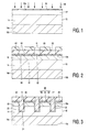
- Figure 1 illustrates an early stage in the manufacture, wherein a p-type region 15' is formed in the low-doped n-type region 14 of the body 10 by implantation of acceptor dopant ions 45, for example of boron.
- acceptor dopant ions 45 for example of boron.
- a thin layer 50 of silicon dioxide may be grown on the silicon body surface 10a, before implanting the ions 45.
- the implantation is carried out in the active cellular area defined by a window in the thick field-oxide layer (not shown).
- a heating step may be carried out to anneal the implant and possibly also to diffuse the implanted dopant to the desired depth for the region portion 15a in the body 10.
- a thin layer 51 of silicon nitride is now deposited on the thin layer 50 of silicon dioxide, followed by a thicker layer 52 of silicon dioxide.
- the nitride layer 51 may have a thickness in the range of 0.1 ⁇ m to 0.2 ⁇ m, whereas the oxide layer 52 is an order of magnitude thicker, for example 1 ⁇ m - 1.5 ⁇ m.
- a photo-resist mask 60 is now provided on the thick oxide layer 52. In the case of a device with an hexagonal cell geometry, this photo-resist mask 60 has a close-packed hexagonal dot pattern. It has windows 61 which define the layout pattern for the trench-gate 11 of the device.
- the insulating layers 52, 51 and 50 are etched away at these windows 61 in the photo-resist pattern 60.
- a grid-shaped window 62 is etched in the layers 50, 51 and 52 which form a mask 65 of insulating material at the major surface 10a of body 10.
- This mask 65 (50, 51, 52) comprises a thicker second layer 52 of a second material (silicon dioxide) on a thinner first layer 51 of an oxidation-masking first material (silicon nitride).
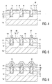
- the window 62 in this mask 65 is now used to form the upstanding insulated trench-gate structure 11, 21 and 22.
- the trench 20 is etched into the body 10 at the window 62.
- the photo-resist mask 60 may still be present during this trench etching stage which may continue directly from the etching of the window 62.
- the trench 20 is etched into the drain region 14, i.e. to a depth greater than the thickness of the region 15'.
- the silicon body 10 is subjected to an oxidation treatment to form a thin silicon dioxide layer 21 on the exposed faces of the trench 20.
- the trench-gate material is now provided in known manner, by depositing doped polycrystalline silicon material 11' to fill the oxidised trenches 20 and windows 62 and to cover the surface of the mask 65 (50, 51, 52).
- the deposited silicon material 11' is then etched back from the surface of the mask 65 (50, 51, 52) until it is left only in the trench 20 and the window 62.
- the resulting structure is illustrated in Figure 3.
- the thick oxide layer 52 is now removed, before using the thinner layer 51 of the oxidation-masking material (silicon nitride) to mask an oxidation treatment which forms an insulating layer 22 of silicon dioxide at an upper part 11 a of the doped silicon gate material 11'.
- this upper part 11 a of the gate material 11' is preferably etched back from the sides of the window 62 to leave the doped silicon gate material 11' upstanding within the window 62 before forming the insulating layer 22 by oxidation.
- This etch-back exposes the polysilicon side area of the upper part 11 a where it locally faces the masking layer 21 and so facilitates the smooth and reliable growth of oxide layer 22 to an adequate thickness at this side area in the following oxidation treatment.
- a thickness of between 0.1 ⁇ m and 0.2 ⁇ m of polycrystalline silicon may be removed from the upper part 11 a by means of this etch-back treatment.
- an oxidation treatment is now carried out to form an insulating overlayer 22 of silicon dioxide over the gate 11 in the trench 20.
- the silicon body areas between the trenches 20 are protected against oxidation by the silicon nitride layer 51.
- the resulting structure is illustrated in Figure 5.
- the thickness of the insulating overlayer 22 may be, for example, in the range of 0.1 ⁇ m to 0.2 ⁇ m
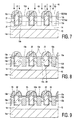
- doped silicon source material 13' is deposited on the upstanding insulated trench-gate structure 11, 21, 22 and on the body region 15' at the exposed surface 10a.
- the resulting structure is illustrated in Figure 6.
- the thickness of the deposited source material 13' may be in the range of, for example, 0.5 ⁇ m to 1.5 ⁇ m.
- the donor dopant concentration of this source material 13' may be in the range of, for example, 10 20 cm -3 to 10 22 cm -3 .
- the layer of deposited source material 13' is now etched-back to leave only the material 13a as a sidewall extension 30 at the sides of the upstanding insulated trench-gate structure 11, 21, 22.
- These doped sidewall extensions 30 are illustrated in Figure 7.
- the sidewall extensions 30 are now used as an implantation mask over the underlying areas of the body 10, while implanting dopant ions 46 (for example of boron) into the body 10 for forming the localised high-doped portion 15b of the body region 15.
- dopant ions 46 for example of boron
- a dose of 10 14 to 5 ⁇ 10 15 cm -2 of boron ions may be used for this implantation.
- the implantation dose is insufficient to over-dope the donor concentration of the sidewall extensions 30 which are to provide at least the bulk of the source region 13.
- the body 10 may be heated to a dopant diffusion temperature for diffusing some of the dopant from the sidewall extension 30 into the body 10.
- the p-n junction 18 of the source region 13 can be moved away from the interface of the deposited doped material 13a and the major surface 10a of the body 10.
- a higher quality p-n junction can be obtained by moving away from this interface.
- the temperature at which the implanted dopant 46 is annealed in the body 10 may also be such as to give rise to some diffusion of the p-n junction 18 as well as the implanted localises portion 15b.
- the localised high-doped portion 15b is preferably implanted and/or diffused to a depth in the body 10 which is greater than the depth of the p-n junction 19a formed by the region 15'.
- the channel-accommodating portion 15a of the body region 15 is formed by the remaining portion of this region 15'.
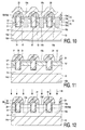
- Figures 8 and 9 illustrate two optional treatments which may be carried out before depositing the source electrode material.
- the doped polycrystalline material 13a of the sidewall extension 30 may be etched back slightly so as to expose a peripheral area of the doped source portion 13b formed in the body 10.
- a silicide-forming metal 55 for example tungsten
- tungsten may be deposited to form a low-resistance silicide contact both to the doped semiconductor material 13a of the sidewall extension 30 and to the adjacent surface area 10a' of the high-doped portion 15b (and the peripheral area of the doped source portion 13b, if exposed).
- tungsten Since tungsten will not react with silicon dioxide, it only forms the silicide with these silicon regions 13a and 10a', so providing a very low sheet resistance for these contacts. Finally, a thick layer of main electrode material (for example aluminium) is deposited to form the source electrode 33.
- main electrode material for example aluminium
- This process of Figures 1 to 10 is particularly suitable for manufacturing devices with a small pitch size and with shallow source and body junctions 18 and 19a.
- the deposited N++ polycrystalline silicon 13a acts directly as a source region of the device, as well as an implant mask for the deep high-doped body portion 15b.
- the process eliminates a source implant step and also saves a photolithographic step for defining the deep body portion 15b.
- Figures 7 to 10 illustrate the high-doped portion 15b as extending deeper than the p-n junction 19a of the channel-accommodating portion 15a, but not extending beyond the bottom of the trench-gate 11.
- the high-doped portion 15b can extend beyond the bottom of the trench-gate 11. This can be achieved in the embodiment of Figures 1 to 10 by using a higher step for the sidewall extension 30 and for the upstanding insulated gate structure 11, 21, 22 and using a higher implantation dose and energy for the dopant ions 46.
- Figures 11 and 12 illustrate another situation in which a higher step can be provided.
- the source region 13 is formed by etching into the major surface 10a of the body 10 through a surface region 13" of the body 10.
- the upstanding insulated trench-gate structure 11, 21, 22 is formed extending through an n-type region 13' of the body 10 as well as through the p-type region 15'.
- the surface region 13" may be formed by implantation and/or diffusion of phosphorus or arsenic in the body 10 to a concentration of at least 5 ⁇ 10 20 cm -3 .
- a sidewall extension 31 of silicon dioxide is provided at the upstanding sides of the insulated trench-gate structure 11, 21, 22.
- This silicon dioxide sidewall extension 31 can be formed using process steps similar to those described in US-A-5,378,655.
- This silicon dioxide sidewall extension 31 covers an area 13a of the surface region 13".
- the structure is illustrated in Figure 11.
- the silicon dioxide sidewall extension 31 is now used as an etchant mask while etching into the surface 10a of body 10 through the thickness of the surface region 13". In this way, a lower surface area 10a' is formed, exposing the p-type region 15'.
- the area 13a of the surface region 13" adjacent to the upstanding insulated trench-gate structure 11, 21, 22 is masked by the silicon dioxide sidewall extension 31 and so is retained to form the source region 13 of the device.
- Figure 12 also illustrates the dopant introduction stage for forming the localised high-doped portion 15b. This may be effected by implantation of boron ions 46, in a manner similar to that of Figure 7.
- the stepped sidewall extension 30 comprises both the doped source region 13a and the silicon dioxide masking portion 31. This step may have a considerable height, permitting a deeper implant of the region portion 15b.
- Figure 12 illustrates the high-doped portion 15b being provided to a greater depth in the body 10 than the bottom of the trench 20.
- the silicon dioxide sidewall extension 31 is etched back (or even etched fully away) before depositing the source electrode 33 to contact both the source region 13a and the body region 15.
- Figure 1 illustrates the preferred situation in which the p-type region 15' for the channel-accommodating portion 15a is provided in the body 10 before the upstanding insulated trench-gate structure 11, 21, 22. However, a modified process is possible in which this region 15' is provided in the body 10 after the insulated trench-gate structure 11, 21, 22.
- the insulating over-layer 22 is formed by oxidising the upper part 11a of the gate electrode material 11'.
- an insulating over-layer 22 over a trench-gate 11 may be formed alternatively by deposition of silicon dioxide or another insulating material.
- the conductive gate 11 is formed of doped polycrystalline silicon, as described above.
- other known gate technologies may be used in particular devices.
- other materials may be used for the gate, such as a thin metal layer which forms a silicide with the polycrystalline silicon material.
- the whole gate 11 may be of a metal instead of polycrystalline silicon.
- Figure 10 illustrates the preferred situation in which the conductive gate 11 is capacitively coupled to the channel-accommodating region portion 15a by a dielectric layer 21.
- Schottky gate technologies may alternatively be used in which a gate dielectric layer 21 is absent and in which the conductive gate 11 is of a metal that forms a Schottky barrier with the low-doped channel-accommodating portion 15a.
- the Schottky gate 11 is capacitively coupled to the channel-accommodating portion 15a by the depletion layer present at the Schottky barrier.
- the insulating over-layer 22 is provided on this Schottky gate 11 so as to form the desired upstanding insulated trench-gate structure 11, 22.
- inventions of Figures 1 to 10 and of Figures 11 and 12 are both for trench-gate devices, for which the invention is particularly advantageous.
- the present invention may also be used for the manufacture of planar/surface-gate devices in which the conductive gate 11' is a planar layer on a gate insulating layer 21' on the major surface 10a of the device body 10.
- An insulating overlayer 22' is present on top of the gate 11' and over the sidewalls of the gate 11'.
- the upstanding sides of the planar gate structure 11',21',22' at the major surface 10a are formed by the insulating overlayer 22' extending over the sidewalls of the gate 11'.
- the sidewall extension 13a' comprising the doped source material is provided.
- This sidewall extension 13a' comprising the doped source material is subsequently used to mask the dopant introduction 46 for providing the deep body portion 15b in accordance with the present invention.
- a p-channel device in which the regions 13 and 14 are of n-type conductivity, the region portions 15a and 15b are of p-type and an electron inversion channel 12 is induced in the region portion 15a by the gate 11.
- a p-channel device can be manufactured by a method in accordance with the invention, in which the regions 13 and 14 are of p-type conductivity, the region portions 15a and 15b are of n-type, and a hole inversion channel 12 is induced in the portion 15a by the gate 11.
Landscapes
- Insulated Gate Type Field-Effect Transistor (AREA)
- Electrodes Of Semiconductors (AREA)
Abstract
Claims (10)
- Procédé de fabrication d'un dispositif de puissance à semi-conducteur comportant une grille connectée de manière capacitive à une partie de réception du canal (15a) d'une zone de corps d'un premier type de conductivité, dans lequel une structure de grille droite est formée au niveau d'une surface principale d'un corps semi-conducteur, la zone de corps du premier type de conductivité s'étendant à côté de la structure de grille pour fournir la partie de réception du canal, une extension de la paroi latérale est prévue sur des côtés droits de la structure de grille pour former un échelon avec une surface adjacente de la zone de corps du premier type de conductivité, l'extension de la paroi latérale comprenant un matériau semi-conducteur dopé du deuxième type de conductivité opposé qui est séparé de la grille par un matériau isolant et qui fournit une zone de source du dispositif, la zone de source formant une jonction PN (18) avec la partie de réception du canal, et une électrode de source est déposée au-dessus de l'échelon de manière à venir en contact avec le matériau semi-conducteur dopé de l'extension de la paroi latérale et la surface adjacente du premier type de conductivité, lequel procédé est caractérisé en ce que la zone de corps comprend également une partie fortement dopée localisée (15b) qui est formée en introduisant un dopant du premier type de conductivité dans le corps semi-conducteur par le biais de ladite surface adjacente en utilisant l'extension de la paroi latérale comprenant le matériau semi-conducteur dopé pour masquer une région sous-jacente dudit corps, la partie fortement dopée présente un niveau de dopage du premier type de conductivité qui est supérieur à celui de la partie de réception du canal mais inférieur au niveau de dopage déterminant la conductivité du matériau semi-conducteur dopé de l'extension de la paroi latérale qui fournit la zone de source, et la partie fortement dopée est déposée plus profondément dans le corps semi-conducteur que la jonction PN entre la zone de source et la partie de réception du canal de la zone de corps et vient en contact avec l'électrode de source au niveau de ladite surface adjacente.
- Procédé suivant la revendication 1, caractérisé en outre en ce que la structure de grille comprend une grille en tranchée formée dans une fenêtre dans un masque au niveau de la surface principale du corps semi-conducteur, dans lequel le masque comprend une deuxième couche plus épaisse (52) d'un deuxième matériau sur une première couche plus mince (51) d'un premier matériau de masquage par oxydation, et la grille en tranchée est faite d'un matériau de grille semi-conducteur dopé, un revêtement isolant est formé dans une partie supérieure du matériau de grille semi-conducteur dopé par oxydation après avoir éliminé la deuxième couche du masque, et l'échelon comprenant l'extension de la paroi latérale est formé après avoir éliminé la première couche.
- Procédé suivant la revendication 2, caractérisé en outre en ce que le matériau de grille semi-conducteur dopé est attaqué chimiquement en retrait sur les côtés de la fenêtre dans le masque pour laisser le matériau de grille semi-conducteur dopé droit dans la fenêtre avant de former le revêtement isolant par oxydation dans la partie supérieure.
- Procédé suivant la revendication 1, 2 ou 3, caractérisé en outre en ce que le matériau de source semi-conducteur dopé du deuxième type de conductivité est déposé sur la structure de grille et sur la zone de corps du premier type de conductivité au niveau de ladite surface principale et est attaqué chimiquement en retrait pour laisser l'extension de la paroi latérale comme zone de source.
- Procédé suivant la revendication 4, caractérisé en outre en ce qu'un dopant provenant du matériau de source semi-conducteur dopé de l'extension de la paroi latérale est diffusé dans le corps semi-conducteur en chauffant le corps semi-conducteur à une température de diffusion de dopant, de manière à éloigner la jonction PN entre la zone de source et la partie de réception du canal de l'interface entre le matériau semi-conducteur dopé déposé et la surface principale du corps semi-conducteur.
- Procédé suivant l'une quelconque des revendications précédentes, caractérisé en outre en ce que le matériau semi-conducteur dopé de l'extension de la paroi latérale comprend du silicium, le corps semi-conducteur au moins adjacent à ladite surface principale comprend du silicium, et un métal formant siliciure est déposé pour former un contact de siliciure à faible résistance à la fois avec le matériau semi-conducteur dopé de l'extension de la paroi latérale et avec la surface adjacente de la partie fortement dopée avant de déposer un matériau d'électrode principale pour l'électrode de source.
- Procédé suivant l'une quelconque des revendications précédentes, caractérisé en outre en ce que le matériau semi-conducteur dopé de l'extension de la paroi latérale est formé en attaquant chimiquement ladite surface principale du corps à travers une zone de la surface du deuxième type de conductivité adjacente à ladite surface principale en masquant une région de ladite zone de la surface adjacente à la structure de grille pour former la zone de source.
- Procédé suivant la revendication 7, caractérisé en outre en ce qu'un motif de masquage qui masque ladite région de ladite zone de la surface pour former la zone de source est présent comme partie de l'extension de la paroi latérale lorsque l'introduction de dopant pour former la partie fortement dopée localisée est effectuée.
- Procédé suivant l'une quelconque des revendications précédentes, caractérisé en outre en ce que la partie fortement dopée localisée est déposée plus profondément dans le corps semi-conducteur que la partie de réception du canal.
- Procédé suivant l'une quelconque des revendications précédentes, caractérisé en outre en ce que le dopant dudit premier type de conductivité pour former la partie fortement dopée localisée est implanté dans le corps semi-conducteur en utilisant l'extension de la paroi latérale comme masque d'implantation au-dessus de la région sous-jacente du corps.
Applications Claiming Priority (3)
| Application Number | Priority Date | Filing Date | Title |
|---|---|---|---|
| GBGB9815021.2A GB9815021D0 (en) | 1998-07-11 | 1998-07-11 | Semiconductor power device manufacture |
| GB9815021 | 1998-07-11 | ||
| PCT/EP1999/004706 WO2000003427A1 (fr) | 1998-07-11 | 1999-07-02 | Fabrication d'un semiconducteur de puissance |
Publications (2)
| Publication Number | Publication Date |
|---|---|
| EP1036411A1 EP1036411A1 (fr) | 2000-09-20 |
| EP1036411B1 true EP1036411B1 (fr) | 2006-06-07 |
Family
ID=10835317
Family Applications (1)
| Application Number | Title | Priority Date | Filing Date |
|---|---|---|---|
| EP99932833A Expired - Lifetime EP1036411B1 (fr) | 1998-07-11 | 1999-07-02 | Fabrication d'un semiconducteur de puissance |
Country Status (7)
| Country | Link |
|---|---|
| US (1) | US6251730B1 (fr) |
| EP (1) | EP1036411B1 (fr) |
| JP (1) | JP2002520851A (fr) |
| KR (1) | KR100562001B1 (fr) |
| DE (1) | DE69931747T2 (fr) |
| GB (1) | GB9815021D0 (fr) |
| WO (1) | WO2000003427A1 (fr) |
Cited By (1)
| Publication number | Priority date | Publication date | Assignee | Title |
|---|---|---|---|---|
| WO2008097642A1 (fr) * | 2007-02-08 | 2008-08-14 | International Rectifier Corporation | Mosfet ayant une capacité d'avalanche améliorée |
Families Citing this family (66)
| Publication number | Priority date | Publication date | Assignee | Title |
|---|---|---|---|---|
| GB9928285D0 (en) * | 1999-11-30 | 2000-01-26 | Koninkl Philips Electronics Nv | Manufacture of trench-gate semiconductor devices |
| JP4906184B2 (ja) * | 2000-11-17 | 2012-03-28 | オンセミコンダクター・トレーディング・リミテッド | 絶縁ゲート型半導体装置の製造方法 |
| US6610143B2 (en) | 2001-01-16 | 2003-08-26 | Semiconductor Components Industries Llc | Method of manufacturing a semiconductor component |
| GB0103715D0 (en) * | 2001-02-15 | 2001-04-04 | Koninkl Philips Electronics Nv | Semicondutor devices and their peripheral termination |
| JP4932088B2 (ja) | 2001-02-19 | 2012-05-16 | ルネサスエレクトロニクス株式会社 | 絶縁ゲート型半導体装置の製造方法 |
| WO2002089195A2 (fr) * | 2001-04-28 | 2002-11-07 | Koninklijke Philips Electronics N.V. | Dispositifs a semiconducteurs a tranchee-grille et leur procede de production |
| GB0117949D0 (en) * | 2001-07-24 | 2001-09-19 | Koninkl Philips Electronics Nv | Trench-gate semiconductor devices and their manufacture |
| US6822288B2 (en) * | 2001-11-20 | 2004-11-23 | General Semiconductor, Inc. | Trench MOSFET device with polycrystalline silicon source contact structure |
| US6753228B2 (en) | 2002-10-15 | 2004-06-22 | Semiconductor Components Industries, L.L.C. | Method of forming a low resistance semiconductor device and structure therefor |
| KR100498476B1 (ko) * | 2003-01-11 | 2005-07-01 | 삼성전자주식회사 | 리세스 채널 mosfet 및 그 제조방법 |
| JP2004228466A (ja) * | 2003-01-27 | 2004-08-12 | Renesas Technology Corp | 集積半導体装置およびその製造方法 |
| KR100500473B1 (ko) * | 2003-10-22 | 2005-07-12 | 삼성전자주식회사 | 반도체 소자에서의 리세스 게이트 트랜지스터 구조 및형성방법 |
| US7400014B2 (en) * | 2004-04-20 | 2008-07-15 | International Rectifier Corporation | ACCUFET with schottky source contact |
| WO2005120913A2 (fr) * | 2004-06-07 | 2005-12-22 | Arne Hjorth Hansen | Dispositif permettant de laver les roues d'un vehicule |
| US7465986B2 (en) * | 2004-08-27 | 2008-12-16 | International Rectifier Corporation | Power semiconductor device including insulated source electrodes inside trenches |
| US7667264B2 (en) * | 2004-09-27 | 2010-02-23 | Alpha And Omega Semiconductor Limited | Shallow source MOSFET |
| US8362547B2 (en) | 2005-02-11 | 2013-01-29 | Alpha & Omega Semiconductor Limited | MOS device with Schottky barrier controlling layer |
| US8283723B2 (en) * | 2005-02-11 | 2012-10-09 | Alpha & Omega Semiconductor Limited | MOS device with low injection diode |
| US8093651B2 (en) * | 2005-02-11 | 2012-01-10 | Alpha & Omega Semiconductor Limited | MOS device with integrated schottky diode in active region contact trench |
| US7948029B2 (en) | 2005-02-11 | 2011-05-24 | Alpha And Omega Semiconductor Incorporated | MOS device with varying trench depth |
| US7285822B2 (en) * | 2005-02-11 | 2007-10-23 | Alpha & Omega Semiconductor, Inc. | Power MOS device |
| AT504998A2 (de) * | 2005-04-06 | 2008-09-15 | Fairchild Semiconductor | Trenched-gate-feldeffekttransistoren und verfahren zum bilden derselben |
| KR100791773B1 (ko) * | 2006-12-27 | 2008-01-04 | 동부일렉트로닉스 주식회사 | 트랜치 게이트 모스 소자 제조 방법 |
| US10062788B2 (en) * | 2008-07-30 | 2018-08-28 | Maxpower Semiconductor Inc. | Semiconductor on insulator devices containing permanent charge |
| US8564057B1 (en) | 2007-01-09 | 2013-10-22 | Maxpower Semiconductor, Inc. | Power devices, structures, components, and methods using lateral drift, fixed net charge, and shield |
| KR20090116702A (ko) * | 2007-01-09 | 2009-11-11 | 맥스파워 세미컨덕터 인크. | 반도체 디바이스 |
| US8884367B2 (en) | 2007-02-08 | 2014-11-11 | International Rectifier Corporation | MOSgated power semiconductor device with source field electrode |
| KR100818111B1 (ko) * | 2007-03-15 | 2008-03-31 | 주식회사 하이닉스반도체 | 반도체 소자 및 그 제조방법 |
| CN101803030A (zh) * | 2007-06-15 | 2010-08-11 | 李泰福 | 半导体功率装置的制造方法 |
| US7923804B2 (en) | 2008-02-14 | 2011-04-12 | Maxpower Semiconductor Inc. | Edge termination with improved breakdown voltage |
| US8076719B2 (en) * | 2008-02-14 | 2011-12-13 | Maxpower Semiconductor, Inc. | Semiconductor device structures and related processes |
| US20090242973A1 (en) | 2008-03-31 | 2009-10-01 | Alpha & Omega Semiconductor, Ltd. | Source and body contact structure for trench-dmos devices using polysilicon |
| WO2009148695A2 (fr) * | 2008-06-02 | 2009-12-10 | Maxpower Semiconductor Inc. | Terminaison de bord pour dispositifs à semi-conducteur |
| WO2009151657A1 (fr) * | 2008-06-11 | 2009-12-17 | Maxpower Semiconductor Inc. | Dispositifs mosfet à super tranchées auto-alignées, procédés et systèmes |
| WO2009154882A2 (fr) * | 2008-06-20 | 2009-12-23 | Maxpower Semiconductor Inc. | Interrupteurs à semiconducteurs à grilles en tranchée |
| US8310001B2 (en) | 2008-07-15 | 2012-11-13 | Maxpower Semiconductor Inc. | MOSFET switch with embedded electrostatic charge |
| WO2010014283A1 (fr) * | 2008-07-30 | 2010-02-04 | Max Power Semiconductor Inc. | Dispositifs latéraux contenant une charge permanente |
| US7960783B2 (en) * | 2008-08-25 | 2011-06-14 | Maxpower Semiconductor Inc. | Devices containing permanent charge |
| US8378416B2 (en) * | 2008-12-01 | 2013-02-19 | Maxpower Semiconductor, Inc. | MOS-gated power devices, methods, and integrated circuits |
| US7989293B2 (en) * | 2009-02-24 | 2011-08-02 | Maxpower Semiconductor, Inc. | Trench device structure and fabrication |
| US8319278B1 (en) | 2009-03-31 | 2012-11-27 | Maxpower Semiconductor, Inc. | Power device structures and methods using empty space zones |
| WO2010120704A2 (fr) * | 2009-04-13 | 2010-10-21 | Maxpower Semiconductor Inc. | Dispositifs à semi-conducteurs électriques, procédés, et structures à couches diélectriques intégrées contenant des charges permanentes |
| US8847307B2 (en) | 2010-04-13 | 2014-09-30 | Maxpower Semiconductor, Inc. | Power semiconductor devices, methods, and structures with embedded dielectric layers containing permanent charges |
| US20110108912A1 (en) * | 2009-11-09 | 2011-05-12 | Hamilton Lu | Methods for fabricating trench metal oxide semiconductor field effect transistors |
| CN102201366B (zh) * | 2010-03-23 | 2013-03-27 | 科轩微电子股份有限公司 | 具有肖特基二极管的沟槽式功率半导体结构及其制造方法 |
| US7994001B1 (en) * | 2010-05-11 | 2011-08-09 | Great Power Semiconductor Corp. | Trenched power semiconductor structure with schottky diode and fabrication method thereof |
| CN102299108B (zh) * | 2010-06-22 | 2014-03-26 | 茂达电子股份有限公司 | 重叠沟槽式栅极半导体组件及其制作方法 |
| US8252648B2 (en) * | 2010-06-29 | 2012-08-28 | Alpha & Omega Semiconductor, Inc. | Power MOSFET device with self-aligned integrated Schottky and its manufacturing method |
| TWI458022B (zh) * | 2010-07-23 | 2014-10-21 | Great Power Semiconductor Corp | 低閘極電荷的溝槽式功率半導體製造方法 |
| JP5738094B2 (ja) * | 2010-09-14 | 2015-06-17 | セイコーインスツル株式会社 | 半導体装置の製造方法 |
| US8754472B2 (en) | 2011-03-10 | 2014-06-17 | O2Micro, Inc. | Methods for fabricating transistors including one or more circular trenches |
| CN102956491B (zh) * | 2011-08-23 | 2015-02-04 | 上海华虹宏力半导体制造有限公司 | 功率晶体管的制造方法 |
| CN102956489B (zh) * | 2011-08-23 | 2015-04-08 | 上海华虹宏力半导体制造有限公司 | 沟槽晶体管的制造方法 |
| CN102956487B (zh) * | 2011-08-23 | 2014-12-10 | 上海华虹宏力半导体制造有限公司 | 隔离型功率晶体管的制造方法 |
| CN102956488B (zh) * | 2011-08-23 | 2015-02-04 | 上海华虹宏力半导体制造有限公司 | 功率晶体管的制作方法 |
| JP5562917B2 (ja) | 2011-09-16 | 2014-07-30 | 株式会社東芝 | 半導体装置及びその製造方法 |
| US9130060B2 (en) | 2012-07-11 | 2015-09-08 | Taiwan Semiconductor Manufacturing Company, Ltd. | Integrated circuit having a vertical power MOS transistor |
| US8669611B2 (en) | 2012-07-11 | 2014-03-11 | Taiwan Semiconductor Manufacturing Company, Ltd. | Apparatus and method for power MOS transistor |
| US8753935B1 (en) | 2012-12-21 | 2014-06-17 | Alpha And Omega Semiconductor Incorporated | High frequency switching MOSFETs with low output capacitance using a depletable P-shield |
| US8809948B1 (en) | 2012-12-21 | 2014-08-19 | Alpha And Omega Semiconductor Incorporated | Device structure and methods of making high density MOSFETs for load switch and DC-DC applications |
| US8951867B2 (en) * | 2012-12-21 | 2015-02-10 | Alpha And Omega Semiconductor Incorporated | High density trench-based power MOSFETs with self-aligned active contacts and method for making such devices |
| US9105494B2 (en) | 2013-02-25 | 2015-08-11 | Alpha and Omega Semiconductors, Incorporated | Termination trench for power MOSFET applications |
| CN104701169A (zh) * | 2013-12-06 | 2015-06-10 | 上海华虹宏力半导体制造有限公司 | 一种抗闩锁的沟槽型绝缘栅双极型晶体管的制造工艺方法 |
| EP3264470A1 (fr) * | 2016-06-29 | 2018-01-03 | ABB Schweiz AG | Mosfet de puissance à tranchée à canal court |
| CN114496785B (zh) * | 2022-04-18 | 2022-08-02 | 深圳芯能半导体技术有限公司 | 一种t型底部保护的沟槽型碳化硅mosfet及其制备方法 |
| CN115207128B (zh) * | 2022-09-09 | 2023-01-13 | 深圳芯能半导体技术有限公司 | 一种沟槽侧壁栅抗负压碳化硅mosfet及其制备方法 |
Family Cites Families (11)
| Publication number | Priority date | Publication date | Assignee | Title |
|---|---|---|---|---|
| JPH0294477A (ja) * | 1988-09-30 | 1990-04-05 | Toshiba Corp | 半導体装置及びその製造方法 |
| JP2606404B2 (ja) * | 1990-04-06 | 1997-05-07 | 日産自動車株式会社 | 半導体装置 |
| KR940002400B1 (ko) * | 1991-05-15 | 1994-03-24 | 금성일렉트론 주식회사 | 리세스 게이트를 갖는 반도체장치의 제조방법 |
| US5268586A (en) * | 1992-02-25 | 1993-12-07 | North American Philips Corporation | Vertical power MOS device with increased ruggedness and method of fabrication |
| GB9207860D0 (en) | 1992-04-09 | 1992-05-27 | Philips Electronics Uk Ltd | A semiconductor component |
| US5300447A (en) * | 1992-09-29 | 1994-04-05 | Texas Instruments Incorporated | Method of manufacturing a minimum scaled transistor |
| GB9306895D0 (en) * | 1993-04-01 | 1993-05-26 | Philips Electronics Uk Ltd | A method of manufacturing a semiconductor device comprising an insulated gate field effect device |
| US5567634A (en) | 1995-05-01 | 1996-10-22 | National Semiconductor Corporation | Method of fabricating self-aligned contact trench DMOS transistors |
| US5684319A (en) * | 1995-08-24 | 1997-11-04 | National Semiconductor Corporation | Self-aligned source and body contact structure for high performance DMOS transistors and method of fabricating same |
| JP3279151B2 (ja) * | 1995-10-23 | 2002-04-30 | トヨタ自動車株式会社 | 半導体装置及びその製造方法 |
| GB9700923D0 (en) | 1997-01-17 | 1997-03-05 | Philips Electronics Nv | Semiconductor devices |
-
1998
- 1998-07-11 GB GBGB9815021.2A patent/GB9815021D0/en not_active Ceased
-
1999
- 1999-07-02 EP EP99932833A patent/EP1036411B1/fr not_active Expired - Lifetime
- 1999-07-02 DE DE69931747T patent/DE69931747T2/de not_active Expired - Fee Related
- 1999-07-02 JP JP2000559588A patent/JP2002520851A/ja not_active Withdrawn
- 1999-07-02 KR KR1020007002542A patent/KR100562001B1/ko not_active Expired - Fee Related
- 1999-07-02 WO PCT/EP1999/004706 patent/WO2000003427A1/fr not_active Ceased
- 1999-07-07 US US09/348,960 patent/US6251730B1/en not_active Expired - Lifetime
Cited By (1)
| Publication number | Priority date | Publication date | Assignee | Title |
|---|---|---|---|---|
| WO2008097642A1 (fr) * | 2007-02-08 | 2008-08-14 | International Rectifier Corporation | Mosfet ayant une capacité d'avalanche améliorée |
Also Published As
| Publication number | Publication date |
|---|---|
| KR20010023861A (ko) | 2001-03-26 |
| KR100562001B1 (ko) | 2006-03-22 |
| DE69931747D1 (de) | 2006-07-20 |
| EP1036411A1 (fr) | 2000-09-20 |
| US6251730B1 (en) | 2001-06-26 |
| GB9815021D0 (en) | 1998-09-09 |
| WO2000003427A1 (fr) | 2000-01-20 |
| JP2002520851A (ja) | 2002-07-09 |
| DE69931747T2 (de) | 2007-06-14 |
Similar Documents
| Publication | Publication Date | Title |
|---|---|---|
| EP1036411B1 (fr) | Fabrication d'un semiconducteur de puissance | |
| US6368921B1 (en) | Manufacture of trench-gate semiconductor devices | |
| EP1393362B1 (fr) | Méthode de fabrication d'un dispositif semi-conducteur à grille en tranchée | |
| US6498071B2 (en) | Manufacture of trench-gate semiconductor devices | |
| US6825105B2 (en) | Manufacture of semiconductor devices with Schottky barriers | |
| US6586800B2 (en) | Trench-gate semiconductor devices | |
| US6043126A (en) | Process for manufacture of MOS gated device with self aligned cells | |
| EP1386352B1 (fr) | Dispositifs semi-conducteurs à grille en tranchée et leur procédé de fabrication | |
| US6087224A (en) | Manufacture of trench-gate semiconductor devices | |
| KR20000013572A (ko) | 트렌치형 파워 모스펫 및 그 제조방법 | |
| US6228698B1 (en) | Manufacture of field-effect semiconductor devices |
Legal Events
| Date | Code | Title | Description |
|---|---|---|---|
| PUAI | Public reference made under article 153(3) epc to a published international application that has entered the european phase |
Free format text: ORIGINAL CODE: 0009012 |
|
| 17P | Request for examination filed |
Effective date: 20000720 |
|
| AK | Designated contracting states |
Kind code of ref document: A1 Designated state(s): AT BE CH CY DE DK ES FI FR GB GR IE IT LI LU MC NL PT SE |
|
| GRAP | Despatch of communication of intention to grant a patent |
Free format text: ORIGINAL CODE: EPIDOSNIGR1 |
|
| GRAS | Grant fee paid |
Free format text: ORIGINAL CODE: EPIDOSNIGR3 |
|
| GRAA | (expected) grant |
Free format text: ORIGINAL CODE: 0009210 |
|
| AK | Designated contracting states |
Kind code of ref document: B1 Designated state(s): DE FR GB IT NL |
|
| PG25 | Lapsed in a contracting state [announced via postgrant information from national office to epo] |
Ref country code: NL Free format text: LAPSE BECAUSE OF FAILURE TO SUBMIT A TRANSLATION OF THE DESCRIPTION OR TO PAY THE FEE WITHIN THE PRESCRIBED TIME-LIMIT Effective date: 20060607 Ref country code: IT Free format text: LAPSE BECAUSE OF FAILURE TO SUBMIT A TRANSLATION OF THE DESCRIPTION OR TO PAY THE FEE WITHIN THE PRESCRIBED TIME-LIMIT;WARNING: LAPSES OF ITALIAN PATENTS WITH EFFECTIVE DATE BEFORE 2007 MAY HAVE OCCURRED AT ANY TIME BEFORE 2007. THE CORRECT EFFECTIVE DATE MAY BE DIFFERENT FROM THE ONE RECORDED. Effective date: 20060607 |
|
| REG | Reference to a national code |
Ref country code: GB Ref legal event code: FG4D |
|
| RBV | Designated contracting states (corrected) |
Designated state(s): DE FR GB IT NL |
|
| REF | Corresponds to: |
Ref document number: 69931747 Country of ref document: DE Date of ref document: 20060720 Kind code of ref document: P |
|
| NLV1 | Nl: lapsed or annulled due to failure to fulfill the requirements of art. 29p and 29m of the patents act | ||
| ET | Fr: translation filed | ||
| PLBE | No opposition filed within time limit |
Free format text: ORIGINAL CODE: 0009261 |
|
| STAA | Information on the status of an ep patent application or granted ep patent |
Free format text: STATUS: NO OPPOSITION FILED WITHIN TIME LIMIT |
|
| REG | Reference to a national code |
Ref country code: FR Ref legal event code: TP |
|
| 26N | No opposition filed |
Effective date: 20070308 |
|
| GBPC | Gb: european patent ceased through non-payment of renewal fee |
Effective date: 20060907 |
|
| PG25 | Lapsed in a contracting state [announced via postgrant information from national office to epo] |
Ref country code: GB Free format text: LAPSE BECAUSE OF NON-PAYMENT OF DUE FEES Effective date: 20060907 |
|
| PGFP | Annual fee paid to national office [announced via postgrant information from national office to epo] |
Ref country code: FR Payment date: 20090710 Year of fee payment: 11 |
|
| PGFP | Annual fee paid to national office [announced via postgrant information from national office to epo] |
Ref country code: DE Payment date: 20090626 Year of fee payment: 11 |
|
| REG | Reference to a national code |
Ref country code: FR Ref legal event code: ST Effective date: 20110331 |
|
| PG25 | Lapsed in a contracting state [announced via postgrant information from national office to epo] |
Ref country code: DE Free format text: LAPSE BECAUSE OF NON-PAYMENT OF DUE FEES Effective date: 20110201 |
|
| REG | Reference to a national code |
Ref country code: DE Ref legal event code: R119 Ref document number: 69931747 Country of ref document: DE Effective date: 20110201 |
|
| PG25 | Lapsed in a contracting state [announced via postgrant information from national office to epo] |
Ref country code: FR Free format text: LAPSE BECAUSE OF NON-PAYMENT OF DUE FEES Effective date: 20100802 |