EP1036443B1 - Trame numerique pour station hertzienne - Google Patents
Trame numerique pour station hertzienne Download PDFInfo
- Publication number
- EP1036443B1 EP1036443B1 EP98955644A EP98955644A EP1036443B1 EP 1036443 B1 EP1036443 B1 EP 1036443B1 EP 98955644 A EP98955644 A EP 98955644A EP 98955644 A EP98955644 A EP 98955644A EP 1036443 B1 EP1036443 B1 EP 1036443B1
- Authority
- EP
- European Patent Office
- Prior art keywords
- signal
- bit rate
- frame
- bits
- signals
- Prior art date
- Legal status (The legal status is an assumption and is not a legal conclusion. Google has not performed a legal analysis and makes no representation as to the accuracy of the status listed.)
- Expired - Lifetime
Links
- 230000001360 synchronised effect Effects 0.000 claims description 65
- 230000005540 biological transmission Effects 0.000 claims description 30
- 238000000034 method Methods 0.000 claims description 18
- 101150078885 CSY3 gene Proteins 0.000 claims description 8
- 101100533082 Zea mays SECY gene Proteins 0.000 claims description 8
- 101150088252 csy1 gene Proteins 0.000 claims description 8
- 101150016576 csy2 gene Proteins 0.000 claims description 8
- 101000714470 Homo sapiens Synaptotagmin-1 Proteins 0.000 claims description 3
- 101000891867 Homo sapiens Synaptotagmin-4 Proteins 0.000 claims description 3
- 102100036417 Synaptotagmin-1 Human genes 0.000 claims description 3
- 102100040817 Synaptotagmin-4 Human genes 0.000 claims description 3
- 230000007423 decrease Effects 0.000 claims description 3
- 101100260765 Schizosaccharomyces pombe (strain 972 / ATCC 24843) tls1 gene Proteins 0.000 claims 1
- 230000015572 biosynthetic process Effects 0.000 description 6
- 238000004891 communication Methods 0.000 description 4
- 230000008569 process Effects 0.000 description 4
- 238000011084 recovery Methods 0.000 description 4
- 238000010586 diagram Methods 0.000 description 3
- 238000005070 sampling Methods 0.000 description 3
- 101100371160 Saccharomyces cerevisiae (strain ATCC 204508 / S288c) TSL1 gene Proteins 0.000 description 2
- 230000008859 change Effects 0.000 description 2
- 238000001914 filtration Methods 0.000 description 2
- 238000003780 insertion Methods 0.000 description 2
- 230000037431 insertion Effects 0.000 description 2
- 238000004519 manufacturing process Methods 0.000 description 2
- 230000033764 rhythmic process Effects 0.000 description 2
- 238000012546 transfer Methods 0.000 description 2
- 230000002457 bidirectional effect Effects 0.000 description 1
- 238000012937 correction Methods 0.000 description 1
- 238000001514 detection method Methods 0.000 description 1
- 238000011161 development Methods 0.000 description 1
- 238000000605 extraction Methods 0.000 description 1
- 238000012423 maintenance Methods 0.000 description 1
- 238000012986 modification Methods 0.000 description 1
- 230000004048 modification Effects 0.000 description 1
- 238000012544 monitoring process Methods 0.000 description 1
- 230000009467 reduction Effects 0.000 description 1
- 238000007493 shaping process Methods 0.000 description 1
- 230000011664 signaling Effects 0.000 description 1
- 230000009897 systematic effect Effects 0.000 description 1
Images


Classifications
-
- H—ELECTRICITY
- H04—ELECTRIC COMMUNICATION TECHNIQUE
- H04J—MULTIPLEX COMMUNICATION
- H04J3/00—Time-division multiplex systems
- H04J3/16—Time-division multiplex systems in which the time allocation to individual channels within a transmission cycle is variable, e.g. to accommodate varying complexity of signals, to vary number of channels transmitted
- H04J3/1605—Fixed allocated frame structures
- H04J3/1623—Plesiochronous digital hierarchy [PDH]
- H04J3/1629—Format building algorithm
Definitions
- the present invention relates to a frame digital with a predetermined duration resulting from the multiplexing of plesiochronous digital signals, as well as a method for forming such a frame.
- the invention is particularly implemented in a radio station which includes a essentially transmitter and receiver equipment digital, located at the base of the station, and a transmission and reception equipment at radiofrequency located for example on the top of a building or pylon and connected by cable from transmission to the first equipment.
- a group of plesiochronous digital signals having normalized flows for example at 2,048 Mbit / s or 8.448 Mbit / s is applied to the equipment transmitter and receiver which multiplexes them into one particular frame.
- To each group of signals plesiochronous corresponds to a radio station special.
- US-A-4,631,720 describes a method for transmitting signals with different bit rates, by time multiplexing, where the frequency of the multiplexed frame is selected as equal to the smallest bit rate of the signals to be transmitted, and one unit signal information with the lowest bit rate is transmitted per frame.
- the present invention aims to reduce the cost of a radio station by introducing circuits which are selectable and programmable in function of plesiochronous signal rates at multiplex into any selected group among several groups of plesiochronous signals, so that the hertzian station is exploitable which whatever the group signal rates selected. More particularly, the invention provides a digital frame of predetermined duration which contributes to achieving this goal.
- a digital frame having a duration predetermined result of signal multiplexing plesiochronous digital is characterized in that that it includes patterns with a structure common and a predetermined length which are independent of digital signal rates plesiochronous to be multiplexed from a selected group among several groups of digital signals plesiochronous with substantially multiple flow rates between them, the patterns comprising bits additional in predetermined number and bits in predetermined number of signals respectively synchronous having multiple bit rates between them and resulting from signal synchronization plesiochronous numbers of the selected group, to each plesiochronous digital signal of the group selected being assigned a number of patterns in the frame equal to the integer part of the quotient of the division of the bit rate of each digital signal plesiochronous of the group selected by the smallest bit rate of plesiochronous digital signals.
- the number of patterns in the frame is equal to the integer part of the division quotient of the sum of the digital signal rates plesiochronous of the group selected by the smallest bit rate of plesiochronous digital signals, and so relatively adapted to customer requests.
- the structure of the frame is modular and the pattern structure is constant whatever the rates of the plesiochronous signals of the groups, this which allows the same circuits to be used in means of transmitting and receiving a station over the air, regardless of signal rate multiplex comprising the frame and corresponding to the group selected. As we will see in the further description of preferred achievements of the invention, these circuits are only programmable based on signal rate multiplex.
- the patterns of the frame have a capacity of constant individual transmission.
- plesiochronous signals at the smaller flows are intended for the same equipment terminal. These can therefore be multiplexed into one synchronous signal.
- said quotient is replaced by the flow division quotient said each plesiochronous digital signal of the group selected by the product of the lowest flow of plesiochronous digital signals and an integer predetermined which is equal to a submultiple of the whole part of the quotient of the division of the flow of plesiochronous signals just above said plus small flow by said smallest flow, a signal synchronous corresponding to the selected group having the lowest throughput resulting from synchronization and multiplexing of plesiochronous digital signals to smallest flow and in number equal to the whole predetermined, and only one reason is assigned in the frame with the smallest synchronous signal debit.
- the additional bits are divided into a lock word, a field constant assignment, an assignment field variable depending on the bit rate of a multiplex signal with the frame corresponding to the group selected, and a correcting code field errors, said fields having lengths respective predetermined.
- the constant assignment field includes example of the frame synchronization bits, and preference of information gathering bits quality errors and / or bits.
- the variable assignment field can include bits of an auxiliary channel whose bit rate offered the higher the signal rate multiplex is high.
- the variable assignment field can also include bits that are reserved to a predetermined number of transmission channels telephone and / or data and which are numerous the lower the bit rate of the multiplex signal is high.
- the variable assignment field can still include bits assigned to a channel telephone service which are in number all the more low that the bit rate of the multiplex signal is high; the constant assignment field then includes a bit signaling a call in the service channel telephone.
- the invention also relates to a method for form the digital frame defined above. It is characterized by the following stages: constitute plesiochronous digital signal groups among several plesiochronous digital signals given having substantially multiple flow rates between them, the sum of the digital signal rates plesiochronous in groups being substantially multiple between them, select one of the groups of plesiochronous digital signals, synchronize the group plesiochronous digital signals selected in synchronous signals having multiple rates between them, assign to each signal synchronous a number of structural patterns predetermined in the frame equal to the whole part of the quotient of the division of the flow of said each synchronous signal by lowest signal rate plesiochronous digital, and form a signal multiplex comprising said frame by inserting into each bit pattern of the respective synchronized signal in predetermined number and additional bits in predetermined number.
- Synchronous signals are obtained by constitution of a frame composed of a word of synchronization, indication bits digital signal justification and bit corresponding plesiochronous so as to raise the flow at a submultiple of the greatest flow of synchronous signals.
- the signals at the smallest speed are synchronized and multiplexed by group of of them.
- said quotient is replaced by the quotient of the division of the flow of said each signal synchronous by the product of the smallest flow of plesiochronous digital signals and an integer predetermined which is equal to a submultiple of the whole part of the quotient of the division of the flow of plesiochronous signals just above said plus small flow by said smallest flow.
- the stage of synchronize plesiochronous digital signals a smaller flow is replaced by a step a multiplex and synchronize digital signals plesiochronous at the lowest rate by equal numbers said quotient of the division of the flow of said each synchronous signal by said product into signals synchronous, when said selected group comprises plesiochronous digital signals to the smallest flow in number equal to at least said quotient.
- the speed of the multiplex signal is at most equal to constant bit rate in the transmission medium, and the signal multiplex is oversampled with a ratio of oversampling between the media flow of transmission and bit rate of the multiplex signal from way to transmit an oversampled signal to the constant flow in the transmission medium which whatever the bit rate of the multiplex signal and therefore whatever the bit rates of digital signals plesiochronous of the selected group.
- the process includes in the equipment to radio frequency, a step of sub-sampling the oversampled signal with the inverse of the ratio of oversampling and a step of selecting frequency filters based on the ratio of oversampling.
- the widths of the strips frequency of selected filters increases with multiplex signal rate.
- inserting the additional bit field into the frame includes word inserts frame alignment, assignment field constant, of a variable assignment field in depending on the bit rate of the selected multiplex signal, and an error correcting code field, said fields with respective lengths predetermined.
- a station radio link basically includes a ETR station transmitter and receiver equipment typically installed inside a building and transmission and reception equipment at ERA radio frequency located either on the roof of the building, or on a pylon near the building.
- the equipment is connected by an AC coaxial cable for bidirectional transmission having a length which can reach a few hundred meters.
- the second ERA device generates a signal microwave at a few gigahertz modulated by the resulting signal from ETR equipment for transmit it through an AN antenna.
- the equipments ETR and ERA also receive a high frequency signal containing a frame modular according to the invention and the demultiplexing of this one in plesiochronous digital signals.
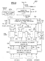
- the first ETR equipment basically includes a digital multiplexing device MUX and a DMUX digital demultiplexing device, one IC1 interface with the AC cable, and a UC microprocessor control with keyboard.
- the second ERA equipment basically includes a IC2 interface, a modulation and transmission circuit high frequency EMC, a subsampling circuit SOE between interface output IC2 and a programmable digital emission filter FIE preceding the EMC circuit, a reception circuit at high frequency CRE, a DU duplexer between CEM and CRE circuits and an AN antenna, a SUE oversampling between a demodulation and FIR digital filtering succeeding the CRE circuit and the IC2 interface, as well as MC microcontroller.
- the frame structure according to the invention transmitted in the AC cable is common to four operating modes M0 to M3 which correspond respectively to numbers of plesiochronous signals at the lowest bit rate at 2.048 Mbit / s equal to the first four powers of 2.
- Aux operating modes correspond respectively to plesiochronous signal groups in table 1 below: FASHION GROUPS M0 2x2 Mbit / s 2 x 2,048 Mbit / s M1 4x2 Mbit / s 4 x 2.048 Mbit / s 8.448 Mbit / s M2 8x2 Mbit / s 8 x 2,048 Mbit / s 4 x 2.048 + 8.448 Mbit / s 2 x 8.448 Mbit / s M3 16 x 2 Mbit / s 16 x 2.048 Mbit / s 12 x 2.048 Mbit / s + 8.448 Mbit / s 8 x 2.048 Mbit / s + 2 x 8.4
- At least two multiplexed signals SC1 to 2.048 Mbit / s, or an SC2 signal at 8.448 Mbit / s, or a SC3 signal at 34.368 Mbit / s are transmitted, and at maximum sixteen SC1 signals at 2.048 Mbit / s, or four 8.42 Mbit / s SC2 signals are multiplexed and transmitted.
- the multiplexing device includes thus at most sixteen inputs for signals SC1, four inputs for SC2 signals and one input for an SC3 signal.
- the sums of the debits of group plesiochronous signals i.e. respective integer products with the lowest throughput plesiochronous signals defining the modes of are multiple.
- the digital multiplexing MUX essentially includes clock decoding and recovery circuits CDR, a CSG group selection circuit, CSY synchronization circuits, a multiplexing and FTH radio frame formation, and an oversampling circuit SUR.
- CDR clock respectively convert plesiochronous signals SC1, SC2, SC3 in line code in incoming plesiochronous binary signals SE1, SE2, SE3 and recover clock signals corresponding to the bit rates of these signals.
- the code in line is for example a bipolar code such as the HDB3 code.
- the CSG group selection circuit includes as many ET circuits as CDR or CSY circuits for select a group of digital signals incoming plesiochronous SE1, SE2, SE3 among groups defined in Table 1.
- the selection of group is controlled by the control unit UC in according to the characteristics entered on the keyboard of the selected group and selected mode Mk, k being an integer between 0 and 3. Signals incoming plesiochronous of the selected group with the corresponding clock signals are only applied to synchronization circuits correspondents through the CSG circuit.
- the incoming plesiochronous signals SE1, SE2, SE3 are synchronized into synchronous signals SY1, SY2, SY3 having flow rates DY1, DY2, DY3 respectively significantly higher than the nominal flow rates DE1, DE2, DE3.
- All synchronization circuits CSY1, CSY2 and CSY3 have an identical structure and their only differ by one programming of frequency dividers by the unit control unit in order to adapt in each circuit clock signals at nominal flow DE1, DE2, DE3 from respective incoming plesiochronous signal SC1, SC2, SC3. Therefore, the synchronization circuits are interchangeable and those in operation are in number determined according to needs, i.e. the number of plesiochronous signals Incoming.
- a synchronization circuit CSY1, CSY2, CSY3 constitutes a module with a circuit decoding and CDR clock recovery and a circuit AND of the CSG group selection circuit. This modular character of the MUX multiplexing device contributes significantly to a reduction in the cost of manufacturing of the first ETR equipment.
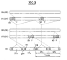
- Synchronization of plesiochronous signals incoming is done by positive justification and phase comparison with clock signals adequate established by a common BT time base.
- the flow DY1, DY2, DY3 of the synchronous signal SY1, SY2, SY3 produced in the corresponding synchronization circuit CSY1, CSY2, CSY3, depends on the one hand, on a systematic insertion bits of an MS synchronization word and bits justification indication IJ in number predetermined by frame of the synchronous signal, and on the other hand an insertion of justification bits positive BJ in order to bridge the difference between the higher constant rate of the synchronous signal and the bit rate of each incoming signal.
- Each sector includes a header including the MS synchronization word and an indication bit of IJ justification for the only plesiochronous signal, or two or more bits of indication of justification corresponding to signals plesiochronous at the same bit-by-bit multiplexed rate, such as two signals SE1 according to the embodiment illustrated in Figure 2.
- the first sector of the frame includes after the header a bit of BJ justification associated with plesiochronous signal respective incoming.
- the other bits in each of sectors are bits of useful signal information incoming plesiochronous.
- the different bit rates, but whole submultiples, synchronous signals make it possible to form frame patterns having a structure established in the FTH circuit, as will be seen below, and common to all the resulting multiplex signals SM0 to SM3.
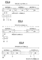
- Figures 4 to 6 respectively show TSY1, TSY2 and TSY3 synchronization frames for synchronous signals SY1, SY2 and SY3 respectively.
- two incoming plesiochronous signals SE1 to DE1 2.048 Mbit / s are synchronized by positive justification by means of two justification bits BJ located in the first sector of the corresponding frame TSY1 in two synchronization circuits CSY1 and multiplexed bit by bit in an MX multiplexer.
- the characteristics of the TSY1 frame with three sectors are indicated in Table 2 below.
- a synchronization circuit CSY2 processes an incoming plesiochronous signal SE2 at 8.448 Mbit / s according to a positive justification method and produces a synchronized signal SY2 having a frame TSY2 shown in FIG. 5.
- the characteristics of the frame TSY2 with five sectors are indicated in Table 3 below.
- a CSY3 circuit processes an incoming plesiochronous signal at 34.368 Mbit / s according to a positive justification method and produces a synchronized signal SY3 having a frame TSY3 shown in FIG. 6.
- the frame TSY3 comprises only a single bit of a word of 10-bit multiframe synchronization included in the first of the six sectors of the frame.
- a multiframe comprises 10 frames.
- the characteristics of the TSY3 frame are indicated in Table 4 below.
- each of the synchronous signals SY1, SY2, SY3 corresponding to the plesiochronous signals of the group selected in the CSG circuit is applied to the multiplexing and frame forming circuit modular so that it is included in one or more elementary patterns.
- Each elementary motif is conforms to the MPEG2 frame recommendation and has a length of 1632 bits, regardless of the group selected and the bit rate of the multiplex signal SMk.
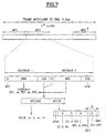
- an elementary pattern is divided into two 816-bit sectors with each 680 bits of useful information from a synchronous signal SY1, SY2, SY3 and 136 bits additional.
- the bits are distributed in a word of 8-bit MVT frame alignment at the start of the sector and into a variable assignment field AV to 120 bits and a constant assignment field at 8 bits at the end of the first sector.
- the extra bits are divided into 8 bits of the constant assignment field at the beginning of the sector, and in a code field 128-bit CCE error corrector, for example a Reed Solomon's code, at the end of the sector.
- each sector 680 locations are occupied by bits of a single synchronous signal equivalent to those of two incoming signals 2.048 Mbit / s low-speed plesiochronous.
- a modular radio frame thus comprises 2 k elementary patterns when the operating mode Mk is selected to produce a multiplex signal SMk at the bit rate DRk, with 0 ⁇ k ⁇ 3.
- the modularity of the frame according to the invention is linked to the modularity of synchronization circuits CSY1, CSY2 and CSY3: the structure of a pattern is constant like that of the synchronization circuit, and the number of patterns in the duration frame constant and the number of synchronization circuits in service are determined based on the number and plesiochronous incoming signal rates at multiplex.
- the frame of the respective multiplex signal has the common radio frame structure shown in Figure 7.
- the bit width in the radio frame is a function of the bit rate of the multiplex signal SMk.
- the output of the ETR equipment is that of the cable interface IC1 which codes the resulting oversampled signal SSURk for example in bipolar code HDB3 and adapts it to the characteristics of the cable AC.
- a bit of the signal SR0, SR1, or SR2 is repeated consecutively 8, 4, or 2 times in the signal SSUR0, SSUR1, or SSUR2 at the DC rate.
- additional BS bits in each frame pattern are split into an 8-bit frame alignment word, a 120-bit AV variable assignment field, a 16-bit AC constant assignment field, and a correcting code field 128-bit CCE errors.
- the AV and AC fields guarantee a minimum and variable transmission capacity as a function of the rate of the multiplex signal SMk for additional transmission channels and identical operation, whatever the mode selected and therefore the 2 k number of frame patterns. Depending on the nature of an additional channel, the number of bits reserved for it is thus variable or constant.
- the AC constant assignment field shown in Figure 7 includes a service channel call bit AVdS telephone, four bits of information of errors E1 to E4, three free bits CL1 to CL3, four frame synchronization bits SYT1 to SYT4, and four Q-quality bits.
- the AVdS bit at a predetermined state signals the operation of a telephone service channel VdS, i.e. a communication in progress establishment or established in the service road VdS telephone whose useful field is included in the variable assignment field AV and has a length inversely proportional to the signal rate SMk multiplex.
- VdS telephone service channel
- the VdS channel ensures the transfer of calls between the transmitting equipment and ETR receivers from two radio stations in communication according to the invention, and preferably the transfer of calls between ETR equipment considered, installed inside the building and transmitting and receiving equipment at ERA radio frequency several hundred metre.
- a telephone communication is established by maintenance service personnel for example, without any other transmission system intermediate.
- Bits E1 to E4 are reserved for collection error information provided by a circuit error correction included in the CRE circuit of ERA equipment. These bits are information local, significant of a motif comprising errors corrected or not, and are inserted in the next pattern.
- the bits E1 to E4 are processed in reception in the station's ETR equipment to estimate the error rate according to the corresponding direction of transmission of the connection radio. For example, bits E1 to E4 indicate that an incorrect byte has been detected and corrected and that a pattern has a number of erroneous bytes greater than the ability to correct Reed Solomon's code, at least 9 bytes, and that these bytes cannot therefore be corrected.
- pairs bits E1-E2 and E3-E4 are assigned to each channel of transmission.
- the three bits CL1 to CL3 remain free for be assigned to new services.
- the four bits SYT1 to SYT4 in each pattern are reserved for frame synchronization wireless modular. These bits complete the word MVT locking of each pattern and contribute to the synchronization of a "multiframe" of patterns actually confused with the modular frame.
- Figures 8, 9 and 10 illustrate the assignment bits of the variable assignment field AV to 120 bits in a pattern respectively depending on the mode M0, M1 mode and M2 or M3 mode.
- auxiliary channel VAux which is processed in an auxiliary channel shaping circuit MFVA ( Figure 2) connected to the FTH circuit according to the operating mode selected under the control of the CPU.
- the data relating to the auxiliary channel is transmitted in the form of a serial signal accompanied by a corresponding clock signal and frame synchronization information.
- Table 5 below shows an example of bit distribution and transmission rates for the auxiliary channel.
- the auxiliary channel signal can be formatted as an auxiliary frame, the structure of which is not predetermined by the modular frame itself but only depends on the application envisaged within the limits of the characteristics of table 5.
- the maximum flow offered to the auxiliary channel is increased at signal rate respective result in the MFVA circuit and is equal to the product of the radio frame frequency of the respective result signal by number of bits available for the auxiliary channel.
- the auxiliary channel VAux transmits an asynchronous signal at 9600 bit / s or a 64 kbit / s signal.
- the VAux channel carries a signal at 256 kbit / s or at least four signals at 64 kbit / s.
- the speed offered to the channel auxiliary VAux here is significantly higher than in previous modes and can transmit up to four 256 kbit / s signals.
- the speed offered to the channel auxiliary VAux is even higher. It is usable to transmit a signal at 2,048 Mbit / s as well as a 256 kbit / s signal or four signals a 64 kbit / s.
- a frame structure divided into three 32-bit sectors is shown in Figure 11. Depending this example the first four bits of each sector are assigned respectively to the four signals at 64 kbit / s, or assigned to the signal at 256 kbit / s.
- the signals are processed in the MFVA circuit in increasing their bit rates according to characteristics of the auxiliary channel.
- the signals asynchronous typically from 4800 to 19200 bit / s are transmitted by oversampling at least 5 times their nominal flow.
- 64 kbit / s or 256 channels kbit / s are transmitted in packets.
- the way to 2048 kbit / s, transmissible only in M3 mode (16 x 2 Mbit / s), is treated as a plesiochronous signal entering. It is inserted in the auxiliary frame after synchronization on the rhythm of it by positive justification.
- variable AV assignment field in each pattern includes 32, 16 or 8 bits in M0, M1, or M2, M3 mode reserved for a network telephone service channel VdSR at 64 kbit / s. Then 4, 2 or 1 bit are assigned to a DIA channel for dialogue between the unit of CPU control in the ETR equipment and the MC microcontroller in the ERA equipment.
- the dialogue includes, in the direction of transmission ETR to ERA, the "rise” of remote controls such as change of plesiochronous signal group and characteristics relative to the selected group, power setting, and in the reception direction ERA to ETR, the "descent" indications of states or faults such as group change, alarms, switching status, received radio field level.
- Each channel DN1, DN2 transmits by oversampling for example a signal asynchronous at 9600 bit / s.
- TSL1 and TSL2 longitudinal remote monitoring are reserved respectively for two lanes of TSL1 and TSL2 longitudinal remote monitoring which ensure a dialogue between devices in a same connection.
- the TSL1 channel is used for the management of the point-to-point wireless link and the TSL2 channel is used for the management of network.
- the 41.732 Mbit / s coded SSURk oversampled signal transmitted by the cable interface IC1 in the coaxial cable CA is decoded in the cable interface IC2 of the radio frequency equipment ERA.
- the SOE subsampling circuit detects each group of 2 3 k consecutive identical bits in the decoded oversampled signal, i.e. each group of 1, 2, 4 or 8 bits for the operating mode M3, M2 , M1 or M0, so as to signal the oversampling ratio 2 3-k to the microcontroller MC and thus sub-sample the signal transmitted through the cable CA with a ratio 1/2 3-k to restore the multiplex signal SMk to the circuit high frequency CEM emission through the digital FIE filter.
- the microcontroller MC programs the digital FIE emission filter in baseband.
- the bandwidths of the programmed filter are compatible with the bit rate DMk of the resulting restored signal SMk corresponding to the selected mode Mk.
- the signal thus filtered modulates a carrier at intermediate frequency which is then transposed to high frequency.
- a digital frame signal microwave at DMk speed is treated according to substantially reciprocal operations of those described in detail above for the broadcast of such a signal.
- the received radio frame signal is amplified, transposed and demodulated into a baseband signal in the high frequency reception circuit CRE.
- the signal received is filtered by frequency filters selected from a battery of filters switchable in the CRE circuit by the microcontroller MC according to the operating mode Mk.
- the signal received in baseband is then filtered according to the operating mode Mk by a programmable filter included in the demodulation and digital FIR filtering circuit.
- the DMUX demultiplexing device After decoding in the cable interface IC1 in the ETR transmitter and receiver equipment, the DMUX demultiplexing device sub-samples the signal received through the AC cable into a digital multiplex signal at the rate DMk according to the sampling ratio 2 3-k relating to the operating mode Mk signaled by the control unit UC. Then, the received multiplex signal is deformatted and demultiplexed into synchronous signals corresponding to the selected group, under the control of the CPU.
- the bits of the AV, AC and CCE fields in each pattern (FIG. 7) of the received multiplex signal are partly processed by the control unit UC to in particular detect errors and generate alarm signals and partly directed to the various VAux, VdSR, VdS, DN1 and DN2 channels.
- the synchronous signals resulting from the demultiplexing of the received multiplex signal are desynchronized by de-gustification, then coded in HDB3 transcoding circuits, into corresponding plesiochronous signals corresponding to
- access to a received component signal at flow rate DE1, DE2 or DE3 can be sufficient under the form of the corresponding synchronous signal SY1, SY2 or SY3.
- Demultiplexing of the received multiplex signal actually consists in extracting from it the patterns corresponding to the desired synchronous signal. Such a extraction is of interest in a radio station intermediate, relay type for most transmitted and switch type signals for signals whose patterns are to be extracted.
Landscapes
- Engineering & Computer Science (AREA)
- Computer Networks & Wireless Communication (AREA)
- Signal Processing (AREA)
- Time-Division Multiplex Systems (AREA)
Description
- fournir plusieurs moyens modulaires de synchronisation pour synchroniser les signaux numériques plésiochrones, et
- mettre en fonctionnement des moyens de synchronisation en nombre égal aux signaux numériques plésiochrones du groupe sélectionné et programmés en fonction des débits de ceux-ci.
- la figure 1 est un bloc-diagramme schématique d'une station hertzienne émettant une trame selon l'invention ;
- la figure 2 est un bloc-diagramme schématique d'un dispositif de multiplexage inclus dans un équipement transmetteur et récepteur de la station hertzienne particulièrement pour la mise en oeuvre du procédé de formation de trame selon l'invention ;
- la figure 3 est un diagramme de signaux illustrant schématiquement la formation de trames de synchronisation pour deux signaux numériques plésiochrones au même débit nominal et la formation d'une trame modulaire selon l'invention, dans le dispositif de multiplexage ;
- les figures 4 à 6 montrent respectivement trois trames de synchronisation pour des signaux synchrones à débits différents produits dans le dispositif de multiplexage ;
- la figure 7 montre une trame modulaire selon l'invention produite par le dispositif de multiplexage ;
- les figures 8 à 10 montrent la composition de champs d'affectation variable respectivement pour des modes de fonctionnement différents du dispositif de multiplexage ; et
- la figure 11 montre une structure de trame d'une voie auxiliaire dans un signal multiplex à débit maximal.
| MODE | GROUPES | |
| M0 | 2x2 Mbit/s | 2 x 2,048 Mbit/s |
| M1 | 4x2 Mbit/s | 4 x 2,048 Mbit/s 8,448 Mbit/s |
| M2 | 8x2 Mbit/s | 8 x 2,048 Mbit/s 4 x 2,048 + 8,448 Mbit/s 2 x 8,448 Mbit/s |
| M3 | 16 x 2 Mbit/s | 16 x 2,048 Mbit/s 12 x 2,048 Mbit/s + 8,448 Mbit/s 8 x 2,048 Mbit/s + 2 x 8,448 Mbit/s 4 x 2,048 Mbit/s + 3 x 8,448 Mbit/s 4 x 8 Mbit/s 34,368 Mbit/s |
| Caractéristiques | Synchronisation dans MX et CSY1 |
| Débit : 2 x SE1 (Mbit/s) | DE1 = 2,048 |
| Débit tramé (Mbit/s) | DY1 = 4,347 |
| Longueur de trame (bits) | 324 |
| Fréquence trame (kHz) | 13,417 |
| Nombre de secteurs | 3 |
| Composition des secteurs : - bits de 2 x SE1 | 102 |
| - bits supplémentaires | 6 |
| Affectation des bits de la trame : | |
| - bits de 2 x SE1 | 2 x 153 |
| - mot de synchronisation MS | 9 |
| - Indication de Justification IJ | 2 x 3 |
| - bits libres BL | 3 |
| Justification par SE1 : | |
| - bit de justification BJ | 1 |
| - taux minimal | 0,3484 |
| - taux nominal | 0,3591 |
| - taux maximal | 0,3697 |
| Caractéristiques | Synchronisation dans CSY2 |
| Débit SE2 (Mbit/s) | DE2 = 8,448 |
| Débit tramé (Mbit/s) | DY2 = 8,694 |
| Longueur de trame (bits) | 540 |
| Fréquence trame (kHz) | 16,101 |
| Nombre de secteurs | 5 |
| Composition des secteurs : - bits de SE2 | 105 |
| - bits supplémentaires | 3 |
| Affectation des bits de la trame : - bits de SE2 | 525 |
| - mot de synchronisation MS | 10 |
| - Indication de Justification IJ | 5 |
| Justification pour SE2 : | |
| - bit de justification BJ | 1 |
| - taux minimal | 0,2705 |
| - taux nominal | 0,2967 |
| - taux maximal | 0,3230 |
| Caractéristiques | Synchronisation dans CSY3 | |
| Trame | Débit SE3 (Mbit/s) | DE3 = 34,368 |
| Débit tramé (Mbit/s) | DY3 = 34, 777 | |
| Longueur de trame (bits) | 534 | |
| Fréquence trame (kHz) | 65, 126 | |
| Nombre de secteurs | 6 | |
| Composition des secteurs : - bits de SE3 | 88 | |
| - bits supplémentaires | 1 | |
| Affectation des bits de la trame : - bits de SE3 | 528 | |
| - mot de synchronisation MS | 1 | |
| - Indication de Justification IJ | 5 | |
| Justification pour SE3 : - bit de justification BJ | 1 | |
| - taux minimal | 0, 2612 | |
| - taux nominal | 0,2823 | |
| - taux maximal | 0,3034 | |
| Multitrame | Longueur de multitrame (bits) | 5340 |
| Nombre de trames | 10 | |
| Affectation des bits de la multitrame | ||
| - SE3 et IJ | 5330 | |
| - mot de synchronisation de multitrame | 10 |
- en mode M0, 20 = 1 seul motif MT1 pour un signal SY2 résultant du multiplexage de deux signaux SE1 à DE1 = 2,048 Mbit/s ;
- en mode M1, 21 = 2 = partie entière de DE2/(2.DE1) motifs MT1 et MT2 attribués respectivemeht à deux paires de signaux SE1 à DE1 = 2,048 Mbit/s, c'est-à-dire à deux signaux synchrones SY1, ou bien à un signal SE2 à DE2 = 8,448 Mbit/s ;
- en mode M2, 21 = 4 = partie entière de 2.DE2/(2.DE1) motifs attribués respectivement à quatre paires de signaux SE1 à DE1 = 2,048 Mbit/s, c'est-à-dire à quatre signaux synchrones SY1 ; ou à deux paires de signaux SE1 et un signal SE2 à DE2 = 8,448 Mbit/s ; ou à deux signaux SE2 ;
- en mode M3, 23 = 8 = partie entière de DE3/(2.DE1) motifs attribués respectivement à 8 paires de signaux SE1 à DE1 = 2,048 Mbit/s, c'est-à-dire à huit signaux synchones SY1 ; ou 6 motifs à 6 paires de signaux SE1 et 2 motifs à un signal SE2, ou 4 motifs à 4 paires de signaux SE1, et deux paires de motifs à deux signaux SE2 ; ou 2 motifs à 2 paires de signaux SE1 et trois paires de motifs à trois signaux SE2 ; ou 4 paires de motifs à 4 signaux SE2 ; ou 8 motifs au signal SE3 à DE3 = 34,368 Mbit/s.
- un bit de défaut DEF pour signaler une perte de verrouillage dans le motif précédent ;
- deux bits d'anomalies AN1 et AN2 pour respectivement signaler un viol de code sur le câble CA et un nombre minimal d'octets erronés dans le motif précédent ;
- un bit de retour de trame erroné RBE correspondant au sens de réception contraire au sens d'émission de la station locale et indiquant la réception d'une trame porteuse d'une indication de motif non corrigé ou de trame comportant au moins un viol de code, ou à la réception d'une trame porteuse d'une indication de perte de verrouillage de trame distante, ou à la détection locale d'une perte de verrouillage de trame.
| Mode (Mbit/s) | Fréquence motif (kHz) | Nbre bits | Débit (kbit/s) | |
| M0 | 2 x 2 | 3,196 | 24 | 76, 7 |
| M1 | 4 x 2 | 6,392 | 72 | 460,2 |
| M2 | 8 x 2 | 12,785 | 96 | 1227,4 |
| M3 | 16 x 2 | 25,571 | 96 | 2454,8 |
Claims (14)
- Trame numérique ayant une durée prédéterminée résultant du multiplexage de signaux numériques plésiochrones, caractérisée en ce qu'elle comprend des motifs (MT1 à MT2k) ayant une structure commune et une longueur prédéterminée qui sont indépendantes des débits de signaux numériques plésiochrones à multiplexer d'un groupe sélectionné parmi plusieurs groupes (M0 à Mk) de signaux numériques plésiochrones (SE1, SE2, SE3) ayant des débits (DE1, DE2, DE3) sensiblement multiples entre eux, les motifs (MT1 à MT2k) comprenant des bits supplémentaires (MVT, AV, AC, CCE) en nombre prédéterminé et des bits en nombre prédéterminé respectivement de signaux synchrones (SY1, SY2, SY3) ayant des débits (DY1, DY2, DY3) multiples entre eux et résultant d'une synchronisation des signaux numériques plésiochrones du groupe sélectionné, à chaque signal numérique plésiochrone du groupe sélectionné étant attribué un nombre de motifs dans la trame égal à la partie entière du quotient de la division du débit dudit chaque signal numérique plésiochrone du groupe sélectionné par le plus petit débit (DE1) des signaux numériques plésiochrones.
- Trame conforme à la revendication 1, dans laquelle ledit quotient est remplacé par le quotient de la division du débit dudit chaque signal numérique plésiochrone du groupe sélectionné par le produit du plus petit débit (DE1) des signaux numériques plésiochrones et d'un entier prédéterminé qui est égal à un sous-multiple de la partie entiere du quotient de la division du débit de signaux plesiochrones juste supérieur audit plus petit débit par ledit plus petit débit, un signal synchrone (SY1) correspondant au groupe sélectionné ayant le plus petit débit (DY1) résultant de synchronisation et multiplexage de signaux numériques plésiochrones (SE1) au plus petit débit (DE1) et en nombre égal à l'entier prédéterminé, et un seul motif étant attribué dans la trame audit signal synchrone (DY1) ayant le plus petit débit.
- Trame conforme à la revendication 1 ou 2, dans laquelle les bits supplémentaires sont répartis en un mot de verrouillage (MVT), un champ d'affectation constante (AC), un champ d'affectation (AV) variable en fonction du débit (DMk) d'un signal multiplex (SMk) comportant la trame correspondant au groupe sélectionné, et un champ de code correcteur d'erreurs (CCE), lesdits champs ayant des longueurs respectives prédéterminées.
- Trame conforme à la revendication 3, dans laquelle le champ d'affectation constante (AC) comprend des bits de synchronisation de trame (SYT1 à SYT4), et de préférence des bits de collecte d'informations d'erreurs (E1-E4) et/ou des bits de qualité (AQ).
- Trame conforme à la revendication 3 ou 4, dans laquelle le champ d'affectation variable (AV) comprend des bits d'une voie auxiliaire (Vaux) dont le débit offert est d'autant plus élevé que le débit du signal multiplex (SMk) est élevé.
- Trame conforme à l'une quelconque des revendications 3 à 5, dans laquelle le champ d'affectation variable (AV) comprend des bits (VSdP, DIA, VdS, DN1, DN2, TLS1, TLS2) qui sont réservés à un nombre prédéterminé de voies de transmission téléphonique et/ou de données et qui sont en nombre d'autant plus faible que le débit du signal multiplex (SMk) est élevé.
- Trame conforme à l'une quelconque des revendications 3 à 6, dans laquelle le champ d'affectation variable (AV) comprend des bits assignés à une voie de service téléphonique (VdS) qui sont en nombre d'autant plus faible que le débit du signal multiplex (SMk) est élevé, et le champ d'affectation constante (AC) comprend un bit (AVdS) signalant un appel dans la voie de service téléphonique.
- Procédé pour former une trame numérique conforme à l'une quelconque des revendications 1 à 7, caractérisé par les étapes suivantes :constituer des groupes de signaux numériques plésiochrones parmi plusieurs signaux numériques plésiochrones donnés (SE1, SE2, SE3) ayant des débits (DR1, DR2, DR3) sensiblement multiples entre eux, les sommes des débits des signaux numériques plésiochrones dans les groupes étant sensiblement multiples entre elles,sélectionner l'un des groupes de signaux numériques plésiochrones,synchroniser les signaux numériques plésiochrones dans le groupe sélectionné en des signaux synchrones (SY1, SY2, SY3) ayant des débits multiples entre eux,attribuer à chaque signal synchrone un nombre de motifs de structure prédéterminée dans la trame égal à la partie entière du quotient de la division du débit dudit chaque signal synchrone par le plus petit débit (DE1) des signaux numériques plésiochrones, etformer un signal multiplex (SMk) comportant ladite trame en insérant dans chaque motif (MT1 à MT2k) des bits du signal synchronisé respectif en nombre prédéterminé et des bits supplémentaires (MVT, AV, AC, CCE) en nombre prédéterminé.
- Procédé conforme à la revendication 8, selon lequel au moins un signal synchrone comporte une trame (TSY2, TSY3) comprenant un mot de synchronisation (MS), plusieurs bits d'indication de justification (IJ) et des bits d'un seul signal numérique plésiochrone correspondant (SE2, SE3).
- Procédé conforme à la revendication 8 ou 9, selon lequel ledit quotient est remplacé par le quotient de la division du débit dudit chaque signal synchrone par le produit du plus petit débit (DE1) des signaux numériques plésiochrones et d'un entier prédéterminé qui est égal à un sous-multiple de la partie entière du quotient de la division du débit de signaux plésiochrones juste supérieur audit plus petit débit par ledit plus petit débit, et selon lequel l'étape de synchroniser des signaux numériques plésiochrones (SE1) au plus petit débit (DE1) est remplacée par une étape de multiplexer et synchroniser les signaux numériques plésiochrones au plus petit débit par nombres égaux audit quotient de la division du débit dudit chaque signal synchrone par ledit produit en des signaux synchrones (SY1), lorsque ledit groupe sélectionné comprend des signaux numériques plésiochrones au plus petit débit en nombre égal au moins audit quotient.
- Procédé conforme à l'une quelconque des revendications 8 à 10, comprenant les étapes de :fournir plusieurs moyens modulaires de synchronisation (CSY1, CSY2, CSY3) pour synchroniser les signaux numériques plésiochrones, etmettre en fonctionnement des moyens de synchronisation en nombre égal aux signaux numériques plésiochrones du groupe sélectionné et programmés en fonction des débits de ceux-ci.
- Procédé conforme à l'une quelconque des revendications 8 à 11, selon lequel le débit du signal multiplex (SMk) est au plus égal au débit constant (DC) dans un support de transmission (CA), et comprenant une étape de suréchantillonner le signal multiplex (SMk) avec un rapport de suréchantillonnage (23-k) entre le débit de support de transmission (DC) et le débit du signal multiplex (DMk) de manière à transmettre un signal suréchantillonné (SSURk) audit débit constant (DC).
- Procédé conforme à la revendication 12, comprenant une étape de sous-échantillonner le signal résultant suréchantillonné (SSURk) avec l'inverse du rapport de suréchantillonnage (23-k) et une étape de sélectionner des filtres de fréquence (CEM) en fonction du rapport de suréchantillonnage, dans un équipement d'émission et de réception à radiofréquence (ERA) d'une station hertzienne relié à un équipement transmetteur et récepteur (ETR) situé à la base de la station hertzienne à travers le support de transmission (CA) et mettant en oeuvre les étapes énoncées dans l'une quelconque des revendications 8 à 12.
- Procédé conforme à l'une quelconque des revendications 8 à 13, selon lequel l'insertion des bits supplémentaires dans la trame comprend les insertions d'un mot de verrouillage de trame (MVT), d'un champ d'affectation constante (AC), d'un champ d'affectation (AV) variable en fonction du débit du signal multiplex, et d'un champ de code correcteur d'erreurs (CCE), lesdits champs ayant des longueurs respectives prédéterminées.
Applications Claiming Priority (3)
| Application Number | Priority Date | Filing Date | Title |
|---|---|---|---|
| FR9715271 | 1997-12-02 | ||
| FR9715271A FR2771872B1 (fr) | 1997-12-02 | 1997-12-02 | Trame numerique pour station hertzienne |
| PCT/FR1998/002417 WO1999029061A1 (fr) | 1997-12-02 | 1998-11-13 | Trame numerique pour station hertzienne |
Publications (2)
| Publication Number | Publication Date |
|---|---|
| EP1036443A1 EP1036443A1 (fr) | 2000-09-20 |
| EP1036443B1 true EP1036443B1 (fr) | 2004-01-28 |
Family
ID=9514141
Family Applications (1)
| Application Number | Title | Priority Date | Filing Date |
|---|---|---|---|
| EP98955644A Expired - Lifetime EP1036443B1 (fr) | 1997-12-02 | 1998-11-13 | Trame numerique pour station hertzienne |
Country Status (6)
| Country | Link |
|---|---|
| EP (1) | EP1036443B1 (fr) |
| BR (1) | BR9815132A (fr) |
| CA (1) | CA2312342A1 (fr) |
| DE (1) | DE69821392T2 (fr) |
| FR (1) | FR2771872B1 (fr) |
| WO (1) | WO1999029061A1 (fr) |
Family Cites Families (3)
| Publication number | Priority date | Publication date | Assignee | Title |
|---|---|---|---|---|
| DE3047045A1 (de) * | 1980-12-13 | 1982-07-29 | Licentia Patent-Verwaltungs-Gmbh, 6000 Frankfurt | Dienstintegriertes uebertragungssystem |
| JPS5833334A (ja) * | 1981-08-21 | 1983-02-26 | Hitachi Ltd | 時分割多重化装置 |
| US4617658A (en) * | 1985-04-17 | 1986-10-14 | Bell Communications Research, Inc. | Frame arrangement for multiplexing a plurality of subchannels onto a fixed rate channel |
-
1997
- 1997-12-02 FR FR9715271A patent/FR2771872B1/fr not_active Expired - Fee Related
-
1998
- 1998-11-13 BR BR9815132-0A patent/BR9815132A/pt not_active IP Right Cessation
- 1998-11-13 WO PCT/FR1998/002417 patent/WO1999029061A1/fr not_active Ceased
- 1998-11-13 CA CA002312342A patent/CA2312342A1/fr not_active Abandoned
- 1998-11-13 EP EP98955644A patent/EP1036443B1/fr not_active Expired - Lifetime
- 1998-11-13 DE DE69821392T patent/DE69821392T2/de not_active Expired - Lifetime
Also Published As
| Publication number | Publication date |
|---|---|
| FR2771872B1 (fr) | 2000-01-07 |
| EP1036443A1 (fr) | 2000-09-20 |
| WO1999029061A1 (fr) | 1999-06-10 |
| FR2771872A1 (fr) | 1999-06-04 |
| DE69821392T2 (de) | 2004-11-04 |
| DE69821392D1 (de) | 2004-03-04 |
| BR9815132A (pt) | 2000-10-10 |
| CA2312342A1 (fr) | 1999-06-10 |
Similar Documents
| Publication | Publication Date | Title |
|---|---|---|
| TW507459B (en) | Air interface frame formats and the method and system for supporting same | |
| EP3343820B1 (fr) | Distribution de signaux de communication sans fil sur des réseaux de télécommunication métropolitains | |
| US7529487B2 (en) | System and method for transmitting data on return path of a cable television system | |
| US5930251A (en) | Multimedia information processing system | |
| US7555008B2 (en) | Method and apparatus for providing a Gigabit Ethernet circuit pack | |
| EP2461623B1 (fr) | Procédé et système pour améliorer la qualité des signaux | |
| JP2001358597A (ja) | エラー訂正符号の構成方法、復号方法、伝送装置、ネットワーク | |
| US20040244049A1 (en) | Cable television system with separate radio frequency hub and ethernet hub | |
| US6389036B1 (en) | Airlink transport container | |
| EP2564530B1 (fr) | Transmission de données impliquant un multiplexage et démultiplexage de signaux d'horloge incorporés | |
| CN106576267A (zh) | 一种数字前传数据的传输方法、设备及系统 | |
| EP1150447B1 (fr) | Procédé et dispositif de transmission et réception de signaux numériques d'ordre élevé à travers deux porteuses radio dans une section de régénération radio | |
| EP1124355B1 (fr) | Mappage de 10 Gigabit-Ethernet pour une interface commune DMP LAN/WAN | |
| AU663590B2 (en) | SDH radio communication system and transmitter/receiver equipment therefor | |
| EP1036443B1 (fr) | Trame numerique pour station hertzienne | |
| US6717958B1 (en) | Video data transmitting/receiving apparatus and method for transmitting video data in a frame structure | |
| EP1036442B1 (fr) | Trame numerique pour station hertzienne | |
| RU2476999C2 (ru) | Передающее устройство радиосвязи и способ радиопередачи | |
| FI102931B (fi) | Verkosta riippumaton kellotus tietoliikennejärjestelmässä | |
| WO2000067408A1 (fr) | Module d'interface de reseau base sur le multiplexage par repartition en longueurs d'ondes denses | |
| CA1324846C (fr) | Noeud regenerateur pour reseau de communication | |
| EP1111829B1 (fr) | Procédé et dispositif de consersion d'un signal STM-1 en un signal sub-STM-1 et vice-versa dans une transmission radio | |
| JP5112302B2 (ja) | イーサネット(登録商標)ネットワークリンクおよびアプリケーション上のクロックレートを転送するための方法およびシステム | |
| Robusto | The development of intermediate data rate (IDR) digital transmission performance characteristics | |
| KR100346784B1 (ko) | 155메가속도급 위성 에이티엠 송수신 신호처리 장치 및 그 방법 |
Legal Events
| Date | Code | Title | Description |
|---|---|---|---|
| PUAI | Public reference made under article 153(3) epc to a published international application that has entered the european phase |
Free format text: ORIGINAL CODE: 0009012 |
|
| 17P | Request for examination filed |
Effective date: 20000425 |
|
| AK | Designated contracting states |
Kind code of ref document: A1 Designated state(s): BE DE ES FI GB IT SE |
|
| 17Q | First examination report despatched |
Effective date: 20021126 |
|
| RAP1 | Party data changed (applicant data changed or rights of an application transferred) |
Owner name: SAGEM S.A. |
|
| GRAP | Despatch of communication of intention to grant a patent |
Free format text: ORIGINAL CODE: EPIDOSNIGR1 |
|
| GRAS | Grant fee paid |
Free format text: ORIGINAL CODE: EPIDOSNIGR3 |
|
| GRAA | (expected) grant |
Free format text: ORIGINAL CODE: 0009210 |
|
| AK | Designated contracting states |
Kind code of ref document: B1 Designated state(s): BE DE ES FI GB IT SE |
|
| PG25 | Lapsed in a contracting state [announced via postgrant information from national office to epo] |
Ref country code: ES Free format text: LAPSE BECAUSE OF FAILURE TO SUBMIT A TRANSLATION OF THE DESCRIPTION OR TO PAY THE FEE WITHIN THE PRESCRIBED TIME-LIMIT Effective date: 20040128 |
|
| REG | Reference to a national code |
Ref country code: GB Ref legal event code: FG4D Free format text: NOT ENGLISH |
|
| REF | Corresponds to: |
Ref document number: 69821392 Country of ref document: DE Date of ref document: 20040304 Kind code of ref document: P |
|
| GBT | Gb: translation of ep patent filed (gb section 77(6)(a)/1977) |
Effective date: 20040216 |
|
| REG | Reference to a national code |
Ref country code: SE Ref legal event code: TRGR |
|
| PG25 | Lapsed in a contracting state [announced via postgrant information from national office to epo] |
Ref country code: BE Free format text: LAPSE BECAUSE OF NON-PAYMENT OF DUE FEES Effective date: 20041130 |
|
| PLBE | No opposition filed within time limit |
Free format text: ORIGINAL CODE: 0009261 |
|
| STAA | Information on the status of an ep patent application or granted ep patent |
Free format text: STATUS: NO OPPOSITION FILED WITHIN TIME LIMIT |
|
| 26N | No opposition filed |
Effective date: 20041029 |
|
| BERE | Be: lapsed |
Owner name: S.A. *SAGEM Effective date: 20041130 |
|
| BERE | Be: lapsed |
Owner name: S.A. *SAGEM Effective date: 20041130 |
|
| REG | Reference to a national code |
Ref country code: GB Ref legal event code: 732E Free format text: REGISTERED BETWEEN 20090319 AND 20090325 |
|
| REG | Reference to a national code |
Ref country code: GB Ref legal event code: 732E Free format text: REGISTERED BETWEEN 20090326 AND 20090401 |
|
| PGFP | Annual fee paid to national office [announced via postgrant information from national office to epo] |
Ref country code: SE Payment date: 20091027 Year of fee payment: 12 Ref country code: FI Payment date: 20091028 Year of fee payment: 12 Ref country code: DE Payment date: 20091126 Year of fee payment: 12 |
|
| PGFP | Annual fee paid to national office [announced via postgrant information from national office to epo] |
Ref country code: IT Payment date: 20091031 Year of fee payment: 12 Ref country code: GB Payment date: 20091102 Year of fee payment: 12 |
|
| REG | Reference to a national code |
Ref country code: SE Ref legal event code: EUG |
|
| GBPC | Gb: european patent ceased through non-payment of renewal fee |
Effective date: 20101113 |
|
| REG | Reference to a national code |
Ref country code: DE Ref legal event code: R119 Ref document number: 69821392 Country of ref document: DE Effective date: 20110601 Ref country code: DE Ref legal event code: R119 Ref document number: 69821392 Country of ref document: DE Effective date: 20110531 |
|
| PG25 | Lapsed in a contracting state [announced via postgrant information from national office to epo] |
Ref country code: FI Free format text: LAPSE BECAUSE OF NON-PAYMENT OF DUE FEES Effective date: 20101113 |
|
| PG25 | Lapsed in a contracting state [announced via postgrant information from national office to epo] |
Ref country code: DE Free format text: LAPSE BECAUSE OF NON-PAYMENT OF DUE FEES Effective date: 20110531 Ref country code: SE Free format text: LAPSE BECAUSE OF NON-PAYMENT OF DUE FEES Effective date: 20101114 |
|
| PG25 | Lapsed in a contracting state [announced via postgrant information from national office to epo] |
Ref country code: GB Free format text: LAPSE BECAUSE OF NON-PAYMENT OF DUE FEES Effective date: 20101113 |
|
| PG25 | Lapsed in a contracting state [announced via postgrant information from national office to epo] |
Ref country code: IT Free format text: LAPSE BECAUSE OF NON-PAYMENT OF DUE FEES Effective date: 20101113 |