EP1039528A2 - In-situ-Methode zur Präparierung und Hervorhebung von Defekten für die Fehleranalyse von Halbleiterchips - Google Patents
In-situ-Methode zur Präparierung und Hervorhebung von Defekten für die Fehleranalyse von Halbleiterchips Download PDFInfo
- Publication number
- EP1039528A2 EP1039528A2 EP00103835A EP00103835A EP1039528A2 EP 1039528 A2 EP1039528 A2 EP 1039528A2 EP 00103835 A EP00103835 A EP 00103835A EP 00103835 A EP00103835 A EP 00103835A EP 1039528 A2 EP1039528 A2 EP 1039528A2
- Authority
- EP
- European Patent Office
- Prior art keywords
- target area
- etching
- sample
- major surface
- dielectric layer
- Prior art date
- Legal status (The legal status is an assumption and is not a legal conclusion. Google has not performed a legal analysis and makes no representation as to the accuracy of the status listed.)
- Withdrawn
Links
Images



Classifications
-
- H—ELECTRICITY
- H10—SEMICONDUCTOR DEVICES; ELECTRIC SOLID-STATE DEVICES NOT OTHERWISE PROVIDED FOR
- H10P—GENERIC PROCESSES OR APPARATUS FOR THE MANUFACTURE OR TREATMENT OF DEVICES COVERED BY CLASS H10
- H10P74/00—Testing or measuring during manufacture or treatment of wafers, substrates or devices
- H10P74/23—Testing or measuring during manufacture or treatment of wafers, substrates or devices characterised by multiple measurements, corrections, marking or sorting processes
- H10P74/238—Testing or measuring during manufacture or treatment of wafers, substrates or devices characterised by multiple measurements, corrections, marking or sorting processes comprising acting in response to an ongoing measurement without interruption of processing, e.g. endpoint detection or in-situ thickness measurement
Definitions
- This disclosure relates to failure analysis and more particularly, to a failure analysis method which preferably employs xenon-difluoride gas for preparing semiconductor chips for the failure analysis.
- Dielectric integrity is always a concern in integrated circuit fabrication.
- Failed semiconductor chips are typically analyzed to discover causes of the failure or failure modes.
- holes formed in thin oxides can be prepared and highlighted by using a two-step process in which a semiconductor chip sample is, in a first step, delayered top-down or cross-sectioned close to a target area to be observed.
- the target area is typically a location believed to be the cause of the failure.
- the delayered top-down or cross-sectioned target area is etched using a selective silicon etch. This is followed by a scanning electron microscopy (SEM) inspection.
- SEM scanning electron microscopy
- a method for inspecting a sample for failures includes the steps of determining a target area for observation on the sample, preparing a region in proximity to the target area to provide access to the target area, and mounting the sample into a chamber.
- the chamber provides a capability for removing material in proximity of the target area, and provides a capability for observing the sample in-situ.
- the sample is maintained in the chamber while performing the following steps: etching a first material selective to a second material such that the target area has the first material removed therefrom to expose the second material such that the second material is preserved for observation, and monitoring the progress of the etching step to determine a time to discontinue the etching.
- the sample may include a major surface, and the first and second materials may be disposed substantially perpendicular to the major surface.
- the step of preparing may then include the step of cutting away material in the region in proximity to the target area to provide access to the target area in a direction perpendicular to the major surface.
- the step of cutting away material may include cutting away material by employing an ion beam.
- the sample may include a major surface and the first and second materials may be disposed substantially parallel to the major surface.
- the step of preparing may include the steps of cleaving the sample to form an edge perpendicular to a layer of at least one of the first material and the second material in the region in proximity to the target area, and providing access to the target area in a direction parallel to the major surface.
- the sample may include a major surface, and the first and second materials may be disposed substantially parallel to the major surface.
- the step of preparing may include the steps of polishing the sample to form an edge perpendicular to a layer of at least one of the first material and the second material in the region in proximity to the target area, and providing access to the target area in a direction parallel to the major surface.
- the sample may include a plurality of layers disposed substantially parallel to a major surface, and the first and second materials may be disposed substantially parallel to the major surface.
- the step of mounting the sample into a chamber may include the step of delayering the plurality of layers to expose the target area.
- the first material may be silicon and the second material may be oxide, nitride or a combination thereof, and the step of etching may include the step of etching the first material selective to the second material with xenon difluoride or with xenon difluoride in the presence of an electron beam.
- the step of monitoring the progress of the etching step may include the step of employing a scanning electron microscope during the etching step to the monitor progress.
- a method for inspecting a semiconductor sample for defects in an insulating layer includes the steps of determining a target area for observation on the semiconductor sample based on a site of a failed device, preparing a region in proximity to the target area to provide access to the target area, and mounting the semiconductor sample into a chamber.
- the chamber provides a capability for removing material in proximity of the target area and provides a capability for observing the semiconductor sample in-situ.
- the semiconductor sample is maintained in the chamber while performing the following steps: removing the material in proximity of the target area, the target area including a dielectric layer having at least one defect therein, wherein a silicon material obscures the at least one defect, etching the silicon material selective to the dielectric layer such that the silicon material is removed from the dielectric layer while the dielectric layer remains substantially intact and monitoring the progress of the etching step to observe the at least one defect.
- the semiconductor sample may include a major surface and the dielectric layer may be disposed substantially perpendicular to the major surface.
- the step of preparing may include the step of cutting away material in the region in proximity to the target area to provide access to the target area in a direction perpendicular to the major surface.
- the step of cutting away material may include cutting away material by employing an ion beam.
- the semiconductor sample may include a major surface, and the dielectric layer may be disposed substantially parallel to the major surface. Then, the step of preparing may include the steps of cleaving the semiconductor sample to form an edge perpendicular to the dielectric layer, and providing access to the target area in a direction parallel to the major surface.
- the semiconductor sample may include a major surface, and the dielectric layer may be disposed substantially parallel to the major surface. Then, the step of preparing may include the steps of polishing the semiconductor sample to form an edge perpendicular to the dielectric layer in the region in proximity to the target area and providing access to the target area in a direction parallel to the major surface.
- the semiconductor sample may include a plurality of layers disposed substantially parallel to a major surface of the semiconductor sample, and the dielectric layer may be disposed substantially parallel to the major surface.
- the step of removing the material in proximity of the target area may include the step of delayering the plurality of layers to expose the target area.
- the step of etching may include the step of etching the silicon material with xenon difluoride or with xenon difluoride in the presence of an electron beam.
- the step of monitoring the progress of the etching step may include the step of employing a scanning electron microscope during the etching step to the monitor progress.
- a method for inspecting and analyzing defects in a dielectric film on a semiconductor chip includes the steps of providing a chamber for inspecting and analyzing the semiconductor chip, the chamber including an ion beam gun and an electron beam gun focused to a substantially same position, mounting the semiconductor chip into the chamber such that a target area includes a dielectric layer with potential defects therein in proximity to the substantially same position, and maintaining the semiconductor chip in the chamber while performing the following steps: removing material in proximity of the target area to expose defects in the dielectric layer, etching silicon material obscuring defects in the dielectric layer selective to the dielectric layer such that the silicon material is removed from the dielectric layer while the dielectric layer remains substantially intact, and monitoring the progress of the etching step to observe the potential defects.
- the chamber may further include an injector for injecting xenon difluoride into the chamber for etching
- the step of etching may include etching the silicon material with xenon difluoride or with xenon difluoride in the presence of an electron beam.
- the step of monitoring the progress of the etching step may include the step of employing a scanning electron microscope during the etching step to monitor the progress.
- the present invention relates to semiconductor failure analysis and more particularly, to a failure analysis method which employs xenon-difluoride gas for preparing semiconductor chips for the failure analysis.
- the present invention provides a method for preparing and highlighting semiconductor samples without removing the sample from the inspection chamber.
- a selective etchant i.e. XeF 2 which is silicon selective
- Si through pinholes in dielectric layers for example, Si0 x ,Si x N y or Si-oxynitride (Si x O y N z ).
- the present invention permits all final preparation and highlighting steps to be done in a dual beam FIB/SEM in-situ.
- a cross-section through a sample may be obtained using a FIB.
- Selective staining may be provided using a XeF 2 injector which may advantageously be included with an inspection chamber.
- the inspection is preferably performed using a SEM, although other tools may be employed.
- the method(s) of present invention may be performed without removing the sample from the chamber.
- the present invention eliminates ex-situ steps and replaces them with in-situ steps in a dual beam (FIB/SEM) chamber for both the staining as well as the delayering/polishing steps.
- the methods of the present invention are very time-efficient and reliable because sample transfer is not necessary once the sample is introduced into the FIB/SEM chamber.
- the delayering and staining steps can be monitored with highest SEM-precision at any time during the process. This eliminates the usual dependencies and uncertainties due to changed external conditions or sample properties conventional methods suffer from.
- Dual beam chamber 10 is shown for performing the method in accordance with the present invention.
- Dual beam chamber 10 may be an XL 830 apparatus, available commercially from FEI Company.
- a dual beam chamber is employed to analyze a dielectric layer in dynamic random access memories (DRAM) or other microchips, in particular microchips printed in sub 0.25um technology.
- Chamber 10 includes an ion gun 12 and an electron gun 14 (which is preferably included on a scanning electron microscope) both focused to a substantially same spot.
- Chamber 10 also includes an etchant injector 16 for introducing etchant gas into chamber 10.
- the etchant gas includes XeF 2 gas although other etchants may be employed.
- Injector 16 is preferably aligned to an electron beam which is introduced by an electron beam gun 14 (SEM).
- Chamber 10 includes a scanning electron microscope 18 or other observation device to advantageously observe samples and their failure modes, or to observe etching processes to chart progress, etc. Chamber 10 is depicted having a failure sample 20 loaded therein. Sample 20 is polished or cleaved on an edge 22 to expose a cross-section of layers on sample 20. In this illustrative example, edge 22 is substantially perpendicular to an ion beam direction shown by arrow "A". In the illustrative example, an insulating layer 24 has a hole 26 which is filled with Si material 28. Edge 22 is created approximately 5 microns or more away from a target area which is centered about a failure site or suspected failure site. Layers 30 on top of insulating layer 24 are removed by the ion beam (FIB).
- FIB ion beam
- Etchant gas preferably includes XeF 2 gas.
- other etchant gases may be employed if they are compatible with chamber 10 and its components and the etchant gas selectively etches a material to be removed relative to a material or feature to be observed. In this case, silicon region 32 is removed selective to the insulating layer 24.
- different components may be viewed by selective etching, for example, conductive components, doped regions, dielectrics, organic compounds etc.
- the etch process is carried out within chamber 10 and can readily be observed. Electrons from an electron beam 34 are used to observe the target are preferably using a SEM. In this way, etching progress may be closely monitored until the features which are desired to be observed by the user are exposed.
- XeF 2 gas has been employed as a source of highlighting FIB cross-sections by selectively etching doped or undoped silicon (Si).
- Si doped or undoped silicon
- the present invention is able to remove any Si covering the insulating layers without noticeably attacking the insulating layer. Holes in thin oxides, for example, may then be highlighted by etching through these holes and by attacking the underlying Si layer as described in the above illustrative example.
- the whole staining process is precisely monitored with the resolution of the scanning electron microscope (SEM) in-situ during the chemical reaction.
- SEM scanning electron microscope
- the etching process may be discontinued at any time to make observations measurements, etc.
- the method of in-situ staining becomes very powerful when combined with the capabilities of a FIB. In this case, the FIB is used to cut close to the target area using the ion beam.
- XeF 2 or equivalent gas is applied to a target surface with the ion beam switched off and the electron beam switched on, discontinuously, to monitor the progress of chemical etching.
- the XeF 2 stain is immune to usual electron raster burn associated with single scans with the electron beam.
- the staining may also be performed in a SEM character only (without ion beam) but equipped with a XeF 2 injector.
- gate oxide holes on 0.2um DRAM technology had to be localized.
- the sample was introduced into chamber 10 and the target area is milled in a fine polishing mode top down using a 150 pA ion beam.
- SEM SEM, it was verified that most of the Poly-Si of the gate stack of the cell transistor was removed and the active area was exposed leaving only a few 10 - 50 nm of silicon above the target area.
- the surface was exposed to XeF 2 gas and the Si-removal was monitored with the SEM. After approximately 2 minutes of total exposure time, a pin hole at the upper edge of the active area was clearly visible proving the suspected fail mechanism of this cell.
- the same method may be applied for the inspection of other dielectric layers, e.g. the isolation of holes in a node dielectric of a deep trench capacitor of a DRAM microchip.
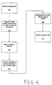
- FIG. 2 a flow diagram is shown for a method of inspecting a semiconductor device in accordance with the present invention.
- the method shown in FIG. 2 is applicable to staining features in layers parallel to a sample's surface (see FIG. 1).
- a sample's surface may be defined by the major surface of a semiconductor chip.
- a target region or area is determined based on component failures or component problems.
- a rough cleave or mechanical polish is performed on a sample to be analyzed.
- the cleave or polish is maintained about 5 microns or more away from a target area or area of interest.
- the sample is mounted within a chamber which includes both an ion beam, for example, FIB and a microscope, for example, an SEM.
- the chamber is a FIBSEM chamber.
- the layers of the sample are mounted parallel to the ion beam direction (from FIB), i.e., perpendicular to the cleaved surface, and transverse to the electron beam direction (for the SEM).
- the layers above the target area are removed preferably using the ion beam.
- the SEM is used to periodically check the sample to identify when the desired region is uncovered or exposed for observation.
- the ion bean is turned off and etchant gas is introduced with or without the electron beam turned on.
- the etchant gas is preferably XeF 2 .
- the area is observed periodically using the SEM to observe etch progress and to observe failures or elements as the case may be.
- etching is stopped upon the uncovering of holes, observation of defects or upon reaching a position to be observed or analyzed.
- a sample 200 may include deep trench capacitors or other vertically disposed components of the semiconductor device.
- Sample 200 includes material to be removed 216 from either or both sides of a target area.
- a silicon region 204 surrounds a trench 206.
- a hole 208 has breached an insulating layer 210 and silicon material 212 from silicon region 204 has filled hole 208 to connect to a region 214 including a silicon compound.
- Area 216 adjacent to silicon region 204 may be removed by ions from an ion gun. This exposes a surface for electrons to fall incident thereon for viewing using a SEM.
- a method for observing sample 200 of FIG. 3 is shown.
- the method shown in FIG. 4 is applicable to staining features in layers perpendicular to a sample's surface (see FIG. 3).
- a sample's surface may be defined by the major surface of a semiconductor chip.
- a target region or area is determined based on component failures or component problems.
- the sample is mounted within a chamber, for example, a FIBSEM chamber. The sample is mounted such that the ion beam is capable of cutting cross-sections in the sample 200, i.e., substantially perpendicular to the major surface of the chip in the direction of arrow "B".
- a deep ion beam cut is performed on either side of the target area until only silicon material of silicon region 204 remains over the target area.
- the SEM is used to periodically check to identify when the desired region is uncovered or exposed for observation.
- etching is stopped upon the uncovering of holes, observation of defects or upon reaching a position to be observed or analyzed.
- etching processes are typically performed outside the chamber in the prior art.
- the etching processes are performed in-situ within the chamber without having to remove and remount the sample.
- the e-beam permits precise monitoring of the etch process, thus minimizing the risk of over-etching.
- the present invention is very selective to particular defects and provides site-specific failure analysis.
- the present invention may be employed in the semiconductor industry or in other industries which perform failure analysis between selectively etchable materials.
- the samples analyzed may include various materials including dielectrics, metal, organic compounds, etc.
Landscapes
- Sampling And Sample Adjustment (AREA)
- Testing Or Measuring Of Semiconductors Or The Like (AREA)
Applications Claiming Priority (2)
| Application Number | Priority Date | Filing Date | Title |
|---|---|---|---|
| US09/277,673 US6162735A (en) | 1999-03-26 | 1999-03-26 | In-situ method for preparing and highlighting of defects for failure analysis |
| US277673 | 2002-10-22 |
Publications (2)
| Publication Number | Publication Date |
|---|---|
| EP1039528A2 true EP1039528A2 (de) | 2000-09-27 |
| EP1039528A3 EP1039528A3 (de) | 2005-10-05 |
Family
ID=23061903
Family Applications (1)
| Application Number | Title | Priority Date | Filing Date |
|---|---|---|---|
| EP00103835A Withdrawn EP1039528A3 (de) | 1999-03-26 | 2000-02-24 | In-situ-Methode zur Präparierung und Hervorhebung von Defekten für die Fehleranalyse von Halbleiterchips |
Country Status (3)
| Country | Link |
|---|---|
| US (1) | US6162735A (de) |
| EP (1) | EP1039528A3 (de) |
| TW (1) | TW461001B (de) |
Cited By (2)
| Publication number | Priority date | Publication date | Assignee | Title |
|---|---|---|---|---|
| EP1419418A4 (de) * | 2001-07-27 | 2006-11-29 | Fei Co | Elektronenstrahlverarbeitung |
| DE102006062015B4 (de) * | 2006-12-29 | 2012-04-26 | Advanced Micro Devices, Inc. | Verfahren zum Testen einer Materialschicht in einer Halbleiterstruktur auf Unversehrtheit |
Families Citing this family (17)
| Publication number | Priority date | Publication date | Assignee | Title |
|---|---|---|---|---|
| KR100345677B1 (ko) * | 1999-12-13 | 2002-07-27 | 주식회사 하이닉스반도체 | 이미지센서의 결함 분석 방법 |
| US6642150B1 (en) | 1999-12-28 | 2003-11-04 | Taiwan Semiconductor Manufacturing Company | Method for testing for blind hole formed in wafer layer |
| US6248603B1 (en) * | 2000-07-13 | 2001-06-19 | Advanced Micro Devices | Method of measuring dielectric layer thickness using SIMS |
| US7088852B1 (en) * | 2001-04-11 | 2006-08-08 | Advanced Micro Devices, Inc. | Three-dimensional tomography |
| JP2004534360A (ja) * | 2001-06-15 | 2004-11-11 | 株式会社荏原製作所 | 電子線装置及びその電子線装置を用いたデバイスの製造方法 |
| US6596553B1 (en) * | 2002-06-26 | 2003-07-22 | Advanced Micro Devices, Inc. | Method of pinhole decoration and detection |
| US7112288B2 (en) * | 2002-08-13 | 2006-09-26 | Texas Instruments Incorporated | Methods for inspection sample preparation |
| TWI240422B (en) * | 2004-10-29 | 2005-09-21 | Promos Technologies Inc | Method of preparing for structural analysis of deep trench capacitors and structural analysis method thereof |
| JP4567487B2 (ja) * | 2005-02-25 | 2010-10-20 | エスアイアイ・ナノテクノロジー株式会社 | 試料観察方法、試料加工方法および荷電粒子ビーム装置 |
| US20070122920A1 (en) * | 2005-11-29 | 2007-05-31 | Bornstein William B | Method for improved control of critical dimensions of etched structures on semiconductor wafers |
| US7744691B2 (en) * | 2007-04-10 | 2010-06-29 | Calcium Silicate Corporation | Energy conserving pozzolan compositions and cements incorporating same |
| US8709269B2 (en) * | 2007-08-22 | 2014-04-29 | Applied Materials Israel, Ltd. | Method and system for imaging a cross section of a specimen |
| GB2480104A (en) * | 2010-05-07 | 2011-11-09 | Plastic Logic Ltd | Device analysis |
| CN107976457B (zh) * | 2017-11-18 | 2020-08-07 | 武汉钢铁有限公司 | 镀锌板表面镀层电子背散射衍射样品制备方法 |
| CN109148316A (zh) * | 2018-09-07 | 2019-01-04 | 北京智芯微电子科技有限公司 | 用于精确判定等离子体刻蚀机刻蚀芯片终点的监测方法 |
| CN113109363B (zh) * | 2021-03-10 | 2022-09-20 | 中国科学院上海微系统与信息技术研究所 | 一种表征硅晶体中缺陷的方法 |
| CN114354665B (zh) * | 2022-03-21 | 2022-05-17 | 晶芯成(北京)科技有限公司 | 一种失效芯片的剥层方法 |
Family Cites Families (7)
| Publication number | Priority date | Publication date | Assignee | Title |
|---|---|---|---|---|
| US4734158A (en) * | 1987-03-16 | 1988-03-29 | Hughes Aircraft Company | Molecular beam etching system and method |
| US5093572A (en) * | 1989-11-02 | 1992-03-03 | Mitsubishi Denki Kabushiki Kaisha | Scanning electron microscope for observation of cross section and method of observing cross section employing the same |
| US5064498A (en) * | 1990-08-21 | 1991-11-12 | Texas Instruments Incorporated | Silicon backside etch for semiconductors |
| US5395769A (en) * | 1992-06-26 | 1995-03-07 | International Business Machines Corporation | Method for controlling silicon etch depth |
| US5399229A (en) * | 1993-05-13 | 1995-03-21 | Texas Instruments Incorporated | System and method for monitoring and evaluating semiconductor wafer fabrication |
| JPH09274883A (ja) * | 1996-04-03 | 1997-10-21 | Hitachi Ltd | Fib/sem複合装置 |
| FR2765031B1 (fr) * | 1997-06-19 | 1999-09-24 | Alsthom Cge Alcatel | Controle de la profondeur de gravure dans la fabrication de composants semiconducteurs |
-
1999
- 1999-03-26 US US09/277,673 patent/US6162735A/en not_active Expired - Lifetime
-
2000
- 2000-02-24 EP EP00103835A patent/EP1039528A3/de not_active Withdrawn
- 2000-09-26 TW TW089105470A patent/TW461001B/zh not_active IP Right Cessation
Cited By (2)
| Publication number | Priority date | Publication date | Assignee | Title |
|---|---|---|---|---|
| EP1419418A4 (de) * | 2001-07-27 | 2006-11-29 | Fei Co | Elektronenstrahlverarbeitung |
| DE102006062015B4 (de) * | 2006-12-29 | 2012-04-26 | Advanced Micro Devices, Inc. | Verfahren zum Testen einer Materialschicht in einer Halbleiterstruktur auf Unversehrtheit |
Also Published As
| Publication number | Publication date |
|---|---|
| TW461001B (en) | 2001-10-21 |
| EP1039528A3 (de) | 2005-10-05 |
| US6162735A (en) | 2000-12-19 |
Similar Documents
| Publication | Publication Date | Title |
|---|---|---|
| US6162735A (en) | In-situ method for preparing and highlighting of defects for failure analysis | |
| US20080054179A1 (en) | Method of fabricating sample membranes for transmission electron microscopy analysis | |
| CN112289795B (zh) | 三维存储器的漏电分析方法及三维存储器 | |
| US7112288B2 (en) | Methods for inspection sample preparation | |
| US6786978B2 (en) | Mass production of cross-section TEM samples by focused ion beam deposition and anisotropic etching | |
| US20210109034A1 (en) | Method for detecting defects in deep features | |
| US6645781B1 (en) | Method to determine a complete etch in integrated devices | |
| US7339391B2 (en) | Defect detection method | |
| GB2302987A (en) | Method for analyzing failure in semiconductor device | |
| Herlinger et al. | TEM sample preparation using a focused ion beam and a probe manipulator | |
| US20120322170A1 (en) | Pinhole inspection method of insulator layer | |
| US6251782B1 (en) | Specimen preparation by focused ion beam technique | |
| US20040016880A1 (en) | Method for the preparation of a TEM lamella | |
| Ruprecht et al. | A review of ULSI failure analysis techniques for DRAMs. Part II: Defect isolation and visualization | |
| US7329550B2 (en) | Method for analyzing the structure of deep trench capacitors and a preparation method thereof | |
| US20080153183A1 (en) | Floating gate process methodology | |
| Nowakowski et al. | An innovative technique for large-scale delayering of semiconductor devices with nanometric-scale surface flatness | |
| US6812049B1 (en) | Method and system for performing failure analysis on a multilayer silicon-on-insulator (SOI) device | |
| US7078247B2 (en) | Early detection of contact liner integrity by chemical reaction | |
| KR100244916B1 (ko) | 반도체 웨이퍼 디펙트 분석방법 | |
| KR100655581B1 (ko) | 투과 전자현미경 분석용 시편의 코팅 장치 및 이를 이용한시편 코팅 방법 | |
| Lau et al. | The application of scanning capacitance microscopy in device failure analysis [doping profile determination] | |
| Zachariasse | CMOS front-end investigation over large areas by deprocessing from the back side | |
| KR100702127B1 (ko) | 반도체소자의 결함검사방법 | |
| US6927082B1 (en) | Method of evaluating the quality of a contact plug fill |
Legal Events
| Date | Code | Title | Description |
|---|---|---|---|
| PUAI | Public reference made under article 153(3) epc to a published international application that has entered the european phase |
Free format text: ORIGINAL CODE: 0009012 |
|
| AK | Designated contracting states |
Kind code of ref document: A2 Designated state(s): AT BE CH CY DE DK ES FI FR GB GR IE IT LI LU MC NL PT SE |
|
| AX | Request for extension of the european patent |
Free format text: AL;LT;LV;MK;RO;SI |
|
| PUAL | Search report despatched |
Free format text: ORIGINAL CODE: 0009013 |
|
| AK | Designated contracting states |
Kind code of ref document: A3 Designated state(s): AT BE CH CY DE DK ES FI FR GB GR IE IT LI LU MC NL PT SE |
|
| AX | Request for extension of the european patent |
Extension state: AL LT LV MK RO SI |
|
| 17P | Request for examination filed |
Effective date: 20060405 |
|
| AKX | Designation fees paid |
Designated state(s): DE FR GB IE IT |
|
| 17Q | First examination report despatched |
Effective date: 20080411 |
|
| STAA | Information on the status of an ep patent application or granted ep patent |
Free format text: STATUS: THE APPLICATION IS DEEMED TO BE WITHDRAWN |
|
| 18D | Application deemed to be withdrawn |
Effective date: 20080822 |