EP1039543A2 - Connecteur d'une puce à circuit et methode de connexion de la meme associée - Google Patents
Connecteur d'une puce à circuit et methode de connexion de la meme associée Download PDFInfo
- Publication number
- EP1039543A2 EP1039543A2 EP00302389A EP00302389A EP1039543A2 EP 1039543 A2 EP1039543 A2 EP 1039543A2 EP 00302389 A EP00302389 A EP 00302389A EP 00302389 A EP00302389 A EP 00302389A EP 1039543 A2 EP1039543 A2 EP 1039543A2
- Authority
- EP
- European Patent Office
- Prior art keywords
- interposer
- subassembly
- chip
- pads
- radio frequency
- Prior art date
- Legal status (The legal status is an assumption and is not a legal conclusion. Google has not performed a legal analysis and makes no representation as to the accuracy of the status listed.)
- Granted
Links
Images

Classifications
-
- G—PHYSICS
- G06—COMPUTING OR CALCULATING; COUNTING
- G06K—GRAPHICAL DATA READING; PRESENTATION OF DATA; RECORD CARRIERS; HANDLING RECORD CARRIERS
- G06K19/00—Record carriers for use with machines and with at least a part designed to carry digital markings
- G06K19/06—Record carriers for use with machines and with at least a part designed to carry digital markings characterised by the kind of the digital marking, e.g. shape, nature, code
- G06K19/067—Record carriers with conductive marks, printed circuits or semiconductor circuit elements, e.g. credit or identity cards also with resonating or responding marks without active components
- G06K19/07—Record carriers with conductive marks, printed circuits or semiconductor circuit elements, e.g. credit or identity cards also with resonating or responding marks without active components with integrated circuit chips
- G06K19/077—Constructional details, e.g. mounting of circuits in the carrier
- G06K19/07749—Constructional details, e.g. mounting of circuits in the carrier the record carrier being capable of non-contact communication, e.g. constructional details of the antenna of a non-contact smart card
- G06K19/0775—Constructional details, e.g. mounting of circuits in the carrier the record carrier being capable of non-contact communication, e.g. constructional details of the antenna of a non-contact smart card arrangements for connecting the integrated circuit to the antenna
- G06K19/07752—Constructional details, e.g. mounting of circuits in the carrier the record carrier being capable of non-contact communication, e.g. constructional details of the antenna of a non-contact smart card arrangements for connecting the integrated circuit to the antenna using an interposer
-
- H—ELECTRICITY
- H10—SEMICONDUCTOR DEVICES; ELECTRIC SOLID-STATE DEVICES NOT OTHERWISE PROVIDED FOR
- H10W—GENERIC PACKAGES, INTERCONNECTIONS, CONNECTORS OR OTHER CONSTRUCTIONAL DETAILS OF DEVICES COVERED BY CLASS H10
- H10W70/00—Package substrates; Interposers; Redistribution layers [RDL]
- H10W70/60—Insulating or insulated package substrates; Interposers; Redistribution layers
- H10W70/62—Insulating or insulated package substrates; Interposers; Redistribution layers characterised by their interconnections
- H10W70/63—Vias, e.g. via plugs
- H10W70/635—Through-vias
-
- H—ELECTRICITY
- H10—SEMICONDUCTOR DEVICES; ELECTRIC SOLID-STATE DEVICES NOT OTHERWISE PROVIDED FOR
- H10W—GENERIC PACKAGES, INTERCONNECTIONS, CONNECTORS OR OTHER CONSTRUCTIONAL DETAILS OF DEVICES COVERED BY CLASS H10
- H10W72/00—Interconnections or connectors in packages
- H10W72/30—Die-attach connectors
-
- H—ELECTRICITY
- H10—SEMICONDUCTOR DEVICES; ELECTRIC SOLID-STATE DEVICES NOT OTHERWISE PROVIDED FOR
- H10W—GENERIC PACKAGES, INTERCONNECTIONS, CONNECTORS OR OTHER CONSTRUCTIONAL DETAILS OF DEVICES COVERED BY CLASS H10
- H10W72/00—Interconnections or connectors in packages
- H10W72/071—Connecting or disconnecting
- H10W72/073—Connecting or disconnecting of die-attach connectors
-
- H—ELECTRICITY
- H10—SEMICONDUCTOR DEVICES; ELECTRIC SOLID-STATE DEVICES NOT OTHERWISE PROVIDED FOR
- H10W—GENERIC PACKAGES, INTERCONNECTIONS, CONNECTORS OR OTHER CONSTRUCTIONAL DETAILS OF DEVICES COVERED BY CLASS H10
- H10W72/00—Interconnections or connectors in packages
- H10W72/071—Connecting or disconnecting
- H10W72/073—Connecting or disconnecting of die-attach connectors
- H10W72/07331—Connecting techniques
-
- H—ELECTRICITY
- H10—SEMICONDUCTOR DEVICES; ELECTRIC SOLID-STATE DEVICES NOT OTHERWISE PROVIDED FOR
- H10W—GENERIC PACKAGES, INTERCONNECTIONS, CONNECTORS OR OTHER CONSTRUCTIONAL DETAILS OF DEVICES COVERED BY CLASS H10
- H10W72/00—Interconnections or connectors in packages
- H10W72/30—Die-attach connectors
- H10W72/321—Structures or relative sizes of die-attach connectors
- H10W72/325—Die-attach connectors having a filler embedded in a matrix
-
- H—ELECTRICITY
- H10—SEMICONDUCTOR DEVICES; ELECTRIC SOLID-STATE DEVICES NOT OTHERWISE PROVIDED FOR
- H10W—GENERIC PACKAGES, INTERCONNECTIONS, CONNECTORS OR OTHER CONSTRUCTIONAL DETAILS OF DEVICES COVERED BY CLASS H10
- H10W72/00—Interconnections or connectors in packages
- H10W72/30—Die-attach connectors
- H10W72/351—Materials of die-attach connectors
-
- H—ELECTRICITY
- H10—SEMICONDUCTOR DEVICES; ELECTRIC SOLID-STATE DEVICES NOT OTHERWISE PROVIDED FOR
- H10W—GENERIC PACKAGES, INTERCONNECTIONS, CONNECTORS OR OTHER CONSTRUCTIONAL DETAILS OF DEVICES COVERED BY CLASS H10
- H10W72/00—Interconnections or connectors in packages
- H10W72/30—Die-attach connectors
- H10W72/351—Materials of die-attach connectors
- H10W72/352—Materials of die-attach connectors comprising metals or metalloids, e.g. solders
-
- H—ELECTRICITY
- H10—SEMICONDUCTOR DEVICES; ELECTRIC SOLID-STATE DEVICES NOT OTHERWISE PROVIDED FOR
- H10W—GENERIC PACKAGES, INTERCONNECTIONS, CONNECTORS OR OTHER CONSTRUCTIONAL DETAILS OF DEVICES COVERED BY CLASS H10
- H10W72/00—Interconnections or connectors in packages
- H10W72/30—Die-attach connectors
- H10W72/351—Materials of die-attach connectors
- H10W72/353—Materials of die-attach connectors not comprising solid metals or solid metalloids, e.g. ceramics
- H10W72/354—Materials of die-attach connectors not comprising solid metals or solid metalloids, e.g. ceramics comprising polymers
Definitions
- the present invention relates to interposers and a method of mounting an integrated circuit chip (IC) or similar device using such an interposer connected across a gap between thin film circuits, such as two conductive film sections of a conductive film antenna, or similar circuit made from conductive film or other conductive flex circuit. More specifically, the invention is directed toward a method of mass-producing devices, such as radio frequency identification tags (RFIDs), by mounting integrated circuit chips (ICs) on interposers that are then physically and electrically connected to the circuit, such as a conductive film antenna, using a pressure sensitive conductive adhesive.
- RFIDs radio frequency identification tags
- Radio frequency (RF) devices such as RFIDs can be used for inventory management, highway toll express passes, and many other purposes that are suited for interrogation of the device.
- RFID devices can be made by incorporating an appropriate IC across the gap of two conductive surfaces of a thin conductive film antenna.
- Such an antenna may be formed by introducing a gap between a conductive film surface, thus creating two conductive portions or halves.
- the IC contains encoded data for identification purposes.
- the IC and the antenna act together as a transponder, which receives an RF signal and modifies it according to the data encoded on the IC.
- the invention is an interposer that includes a thin substrate having two printed conductive ink pads. These pads provide a larger effective electrical contact area than ICs precisely aligned for direct placement without an interposer. The larger area reduces the accuracy required for placement of ICs during manufacture while still providing effective electrical connection.
- the substrate is coated with a pressure sensitive conductive adhesive that allows an IC to be electrically and mechanically mounted across the conductive ink pads. Pressure sensitive adhesives are preferred, but this production method is not limited only to pressure sensitive applications.
- the IC can be mounted across the gap of the interposer, ideally with the same adhesive as used to mount the interposer-IC subassembly to the circuit.
- IC placement was accomplished by first placing the individual base substrate in alignment with an IC, such that the bonding leads of the substrate are aligned to the connectors on the IC. Alternately, if the substrate is the base piece, the IC had to be precisely aligned for a physical and electrical connection.
- the relatively small bonding leads or pads on the substrate and IC provide a small effective connection area and greatly restrain the tolerances for placement of an IC across the gap of a thin metallic film circuit substrate. IC placement and mounting are serious limitations for high speed manufacturing.
- a prior method of making a RF tag includes using a chip placement machine that mounts ICs between two separate conductive portions of a thin film antenna. This method requires the precise alignment of the IC between a gap of approximately 0.017 inch between the antenna portions. Such tolerances greatly reduce line speeds. This method is acceptable for high-priced items that can be produced at slow line speed.
- the chip placement machine cannot be readily used for high speed application of ICs on low cost devices. Also, a chip placement machine is relatively costly to purchase and operate.
- the interposer with a pre-positioned IC overcomes this required precision so that a convertor, such as a label printer, can affix ICs with a high line speed as required for uses such as packaging or other disposable products incorporating RFID tags or similar devices.
- a converter can use existing technology to apply the IC mounted on an interposer without the need to purchase a chip placement machine.
- the adhesive of the present invention is printed over the conductor area and serves to attach the interposer to the antenna halves, both physically and electrically. It may be printed or applied in any pattern including having an aperture or recess.
- the replacement of solder bond connections by anisotropic conductive adhesives can often reduce assembly costs, can accommodate relatively high concentrations of conductive connections, and can make devices more amenable to repair and reconstruction. Similar techniques are needed to bond ICs to thin film circuit substrates, such as antenna halves, without significant curing times, without excessive heat, and without matching bonding raised areas in precise alignment.
- the present method uses pressure sensitive anisotropically conductive adhesive between the IC mounted on an interposer and the antenna halves (base substrate) to solve these concerns. Pressure sensitive adhesives are selected for ease of application, but other adhesives are available though not preferred.
- the ICs were previously encapsulated by the application of a chip face encapsulant material on the ICs that are attached to the antenna.
- an epoxy was used. Besides long curing times, the use of epoxy may cause undesirable friction when joining circuits to an interposer.
- the present interposer can secure the IC, rather than placing an epoxy encapsulant over the surface of the IC.
- the curing of an epoxy encapsulant often takes hours and is not conducive to high speed production.
- the present invention overcomes the long cure time of such encapsulants by using a pressure sensitive conductive adhesive and an interposer that can secure the IC.
- filled epoxy is more rigid so devices requiring flexibility are not well suited for epoxy encapsulants over the surface of the IC.
- the interposer of the present invention maintains flexibility.
- ICs have become drastically less expensive, and are often not the most expensive part of a device.
- An IC may be incorporated into a device, such as an RFID tag, a luggage tag or prescription label, in which the device substrate would be the most expensive component.
- the "expensive device substrate,” for lack of a better term, can be spoiled if the IC is not mounted correctly or if there is a short circuit in the mounted IC. Isolating the IC placement to the less expensive interposer subassembly allows IC defects to be detected before the final assembly to the more expensive device substrate, such as a thin film antenna. An IC on an interposer will make for less spoilage of the "expensive device substrate.” Spoilage is limited to the lowest cost component when a low-cost interposer with an IC is used.
- interposer-chip combination This relates to another critical problem overcome by the interposer-chip combination. Certain applications require sequential production of expensive device substrates, such as numbered pharmaceutical labels or packages. If a bad IC is inserted in such a sequence-critical application, the web would have to be re-spliced, effectively shutting down production until completed. By isolating the individual interposer-chip combination as a subassembly, the interposer can be applied by a standard head that can repeat without shutting down when a bad IC is detected so that there are no missing labels or packages in the sequence.
- interposer that is inexpensive to mass produce and easy to insert at high line speed, preferably in multiple orientations with respect to the antenna or similar circuit.
- the present invention incorporates some of the advantages of the existing technology, while alleviating several of the problems associated therewith. Interposers are well suited for high volume applications because they offer low-cost solutions and easy attachment. Additionally, the improved method of manufacturing a thin RF transponder with such an interposer is necessary for such mass production.
- the invention may be described as a method of making thin, flexible transponders, such as RFID labels and tags.
- RFIDs require an RF antenna and an appropriate IC encoded with data.
- the present invention uses an interposer having an IC as a subassembly that is attached to a thin conductive film antenna.
- An RF antenna is formed by creating a gap between two portions of metal on a thin metallic film. The gap may be formed by using a laser or by masking the gap before the metallic film is applied to the thin film.
- the IC via an interposer is connected across the gap between the antenna portions, thus creating an RFID. No wiring or heating is required because the interposer has two pads, such as carbon ink printed, that make electrical contact with the isolated antenna portions, via an electrically conductive adhesive.
- a pressure sensitive adhesive will not require significant curing time for attachment to become effective.
- an IC is not directly mechanically and electrically attached to the antenna.
- the IC is attached to an interposer so that it can be positioned at the connection ends of the antenna circuit.
- the interposer comprises a base substrate film with two printed pads. An IC is connected between the two electrically isolated pads.
- the interposer can provide added structural support and can secure the internal components.
- Other flush mount components, such as LEDs, can be attached using similar techniques. This removes the limitations for precise placement on the leads of a circuit. Additionally, IC's can be mounted on conventional circuits via an interposer.
- Placement of the IC is easier with the interposer.
- the gap between antenna portions is critical for proper functioning of an RF antenna.
- the antenna gap is dictated by the spacing between the IC pads and requires the IC to be precisely inserted (by machine placement for instance) between a space of 0.014 and 0.020 inch, which is a typical gap between IC pads.
- the interposer isolates the IC placement to this critical gap by limiting it to a subassembly having a critical gap created between two relatively large separate conductive interposer pads.
- the IC is placed across the critical gap between the interposer pads. Since the connector pads of the interposer can contact any portion of the antenna pad to establish electrical connection, placement of the interposer is not constrained by the relatively small critical interposer gap.
- the interposer pads still maintain an electrical connection across the non-critical antenna gap. This removes the IC placement constraint created by the critical antenna gap located on the antenna circuit substrate while maintaining the function of the critical gap in the circuit.
- the larger area of the interposer pads reduces the accuracy required for placement of ICs during manufacture while still providing effective electrical connection. This allows an IC to be placed across the gap with greater placement tolerances.
- An example of such an interposer pad would be a printed carbon ink that is 0.20 inches extended from the IC connection area. Silver is an expensive substitute for carbon ink and the tolerance can dictate the necessary extension of the pad from the IC connection area. It is contemplated that the carbon ink or silver ink pad is not printed on the entire interposer surface.
- insertion can be used with many devices.
- the interposer pattern or repeat is constant thereby simplifying the critical IC placement step. There is still a critical gap, but it is in a constant format. Variability of the antenna pattern adds significant complexity to the direct IC attachment process. For example, tickets, luggage tags, anti-theft devices or inventory control devices have different layouts for antennas or other circuits. Direct attachment would require a reconfiguration for each different antenna or circuit layout.
- the finished part can vary widely and not encumber the process.
- interposer-chip subassemblies are prepared for subsequent attachment to antennas by starting with numerous printed interposers on a web to which a plurality of ICs is attached. Nearly 1000 interposers can be placed on each foot of web with a width of 18 inches. Preferably, each interposer-chip subassembly is separate and rectangular for easy application like a label.
- the group of interposer-chip subassemblies is inexpensive to mass produce and easy to insert at high line speed with less spoilage of devices due to defective ICs.
- the interposers are designed for a minimum press speed of 80 feet per minute.
- This invention also includes a geometry of components that allows for attachment of the interposer chip subcomponent regardless of the orientation of the antenna or similar circuit to which it is attached.
- Current IC mounting technology requires the IC be mounted across the interposer gap. Interposers are inserted in the web direction to be accurately placed on the antenna or similar circuit. The gap must presently be perpendicular to the interposer web direction due to IC orientation. Therefore, without the improved geometry, the interposer reel must be oriented parallel to the antenna web being printed.
- the antenna gaps may be desirable to orient the antenna gaps either parallel or perpendicular to the web direction during printing or application. In fact, in extreme cases, it may be desirable to orient the antenna gaps at angles other than 0° or 90° to the web, in which case, current geometries fail.
- the improved geometry includes conductive ink pads that are in the shape of a butterfly, propeller or bow-tie pattern preferably with a separation line between each portion.
- the butterfly, propeller or bow-tie pattern extends from one corner of the label to the opposite corner.
- the pattern must maintain a gap perpendicular to the web to allow for IC placement across the gap.
- a conductive adhesive is printed or applied around the edges of the label with a recess of no adhesive in the center.
- a metallized film package can be used as an antenna for an RFID device.
- Metallized films and papers are common components of packaging and labels used for barrier properties, opacity, and desirable graphics. Due to the conductivity of a metallized surface, the material can function as a RF antenna. With a laser, metal can be removed from the package film, but leaving the base film intact, so that there are two electrically and physically isolated portions of metallic surface. A gap must be incorporated between the portions to provide electrical isolation.
- Another non-conductive substrate, such as a paper or polymer could be laminated to the metallized film so that the packaging maintains two electrically isolated surfaces.
- An appropriate integrated circuit article preferably using an interposer will convert the package into an RFID device (or a similar device) if access to the portions of the metallized surface is available.
- the interposer can be applied to the package (RFID antenna) as described herein to replace the less versatile bar code.
- a separate substrate of the device that contains an antenna layer would not be required because the metallized film layer forming the antenna is a portion of the packaging film.
- a thin film circuit shown as an antenna 20 (or a similar circuit made from metallized film or other metallized flex circuit) can be made from a thin etched or stamped foil, typically manufactured from a thin foil of copper, copper-alloy, or nickel-iron alloy by stamping or etching. The etching or stamping creates patterns on strips that become antennas.
- Other methods of making an antenna include printing a conductive ink. This invention relates to ICs 10, which are joined and electrically connected to individual antennas 20, focusing on the interposer 30, its substrate 32, and the printing of contact pads 34 and 36 thereon onto which the IC 10 is incorporated.
- the layer of anisotropically conductive pressure sensitive adhesive 38 makes contact with connectors of the IC 10 as to interconnect the antenna 20 and the IC 10.
- Pressure sensitive adhesives are selected for ease of application, but other adhesives are available though not necessarily preferred. Two different adhesives, both conductive, can be used in association with the interposer 30. A pressure sensitive conductive adhesive is preferred for attachment of the interposer 30 to the antenna 20 or similar circuit, and a different adhesive can be used to attach the IC 10 to the interposer 30, such as a conductive hot melt.
- the subassembly includes IC 10 on the interposer 30 such that the IC 10 is in contact with both pads 34 and 36 of the interposer 30.
- the subassembly is adhered to a base circuit substrate to form a device.
- the subassembly is adhered to a thin metallic film antenna 20 to form an RFID.
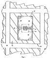
- Figure 1 shows an interposer 30 having a substrate 32 (on a matrix web 40) with an attached IC 10.
- the interposer 30 is ideally as small as possible such as .400 inches square, not including the matrix web portion (which is typically 0.060 inches in length between each interposer).
- the interposer 30 preferably has a geometric shape, such as a rectangle or square, that allows for ease of insertion by a standard press head.
- An eighteen-inch web can contain thirty-six interposers 30 across for use in mass production.
- Figure 1 indicates a raised non-contact area 44 of the interposer 30 around the IC 10 resulting from the height of the IC 10.
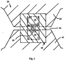
- the non-contact area 44 is created when the interposer 30 is applied across a gap 66 of a thin metallic film antenna 20, as shown in FIG. 2.
- This raised area 44 assumes a height of 0.006 inch for the IC and a ten-degree contact angle.
- the interposer substrate 32 can be a variety of film or paper. Flexible substrates, such a polymeric film or paper, are preferred. Ideally, the surface of the substrate 32 is ink-receptive if a carbon pad (34 or 36) or a similar pad is printed.
- the pads 34 and 36 are conductive surfaces that are designed to make electrical contact with antenna portions 60 and 62. Pads 34 and 36 provide a large effective electrical contact, which reduces the accuracy required for placement of ICs during manufacture while still providing effective electrical connection. As shown in Figure 1, the pads 34 and 36 would conduct only in a direction transverse to pads 34 and 36. The pads 34 and 36 physically and electrically contact the antenna portions 60 and 62, via conductive (preferably pressure sensitive) adhesive 38, as shown in Figure 2. There is a gap 46 between the pads 34 and 36 so that they are electrically isolated surfaces. The gap 46 between the pads 34 and 36 is not as critical as the gap 66 between antenna portions 60 and 62, which makes it easier to insert the IC 10 attached to an interposer 30. As shown in Figure 1, the carbon ink area of the pads (34 and 36) is 0.04 square inches (0.2 by 0.2 inch for each pad).
- the pads 34 and 36 are silver or carbon printed.
- Known printing techniques such as flexographic, screen, or rotogravure are suitable.
- the preferable resistance is less than 100 ohms per square. (Resistivity is measured on a strip with a 10:1 length to width ratio. Ohm/square is determined by dividing the resistance measurement along the length by 10.)
- the choice of material depends on the costs and level of conductivity required. The lowest possible resistance is ideally preferred.
- Carbon is approximately 100 ohms per square compared to less than one ohm per square for silver, but silver is approximately ten times as expensive.
- Certain metallized films (i.e., vapor deposited) and foils have greater conductivity.
- leading edge 45 of the printed pad 36 can serve as an alignment mark in printing. As shown in Figure 1, leading edge 45 is 0.200 inch in length. It does not extend the whole length of the substrate 32 and is representative of a printed carbon ink.
- the pads 34 and 36 may be smaller if a more conductive material such as silver is used.
- the carbon ink or silver ink pad need not be printed on the entire interposer surface.
- a conductive adhesive film 38 secures the components of the device, such as an RFID tag.
- the conductive adhesive can be applied or printed over any conductor including metallized film, printed conductive inks (either carbon or silver or combinations thereof), foils or other conductors. Ideally, the same adhesive can be used to mount and hold the IC 10 that bonds the device together.
- a pressure sensitive anisotropically conductive adhesive is most desirable to mount the IC 10 to the interposer 30, as well as to bond the resulting tag or device together.
- the conductive adhesive is preferably printable.
- the pressure sensitive adhesive film 38 will adhere the components together with an electrically conductive film that transmits current only anisotropically.
- the conductive adhesive may also serve to hold the interposer 30 to a liner, which allows handling of interposers 30 in roll form to be applied as labels from reels.
- the adhesive properties of the conductive adhesive are adjusted with the liner to facilitate the handling of interposers during IC attachment and to provide release properties to allow mechanical insertion in high volume applications.
- the pressure sensitive adhesive does not require the application of heat to adhere the components.
- the pressure sensitive adhesive can be cured through radiation (UV or EB) or can be conventionally dried (either as solvent-based or water-based). UV cured adhesives have been used as the preferred curing/drying method, and for high-speed production, a quick curing solution is required. H.B. Fuller has a part for such a formula, namely Solar Cure RT-7575.
- the anisotropically conductive adhesive is a printable, UV-quick curable, pressure sensitive adhesive that maintains its flexibility. Adhesives to be avoided include those that require UV, heat or microwave curing that have an unacceptable cure time for high speed production.
- the pressure sensitive adhesive film 38 ideally has a minimal resistance, but metal or other conductors adversely affect the adhesion.
- the pressure sensitive adhesive film 38 must be suitable for high speed applications, such as having properties that avoid bubbling.
- the adhesive must provide sufficient bonding and electrical properties at a high speed insertion. It should preferably maintain flexibility without losing its connection.
- the adhesive is preferably printed over the conductor area and serves to attach the interposer to the antenna halves, both physically and electrically.
- the adhesive can be printed either by flexographic, gravure or screen printing or other suitable printing methods.
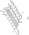
- Figure 3 is an expanded perspective view of a label 82, conductive ink 83 with two pads 84 and 86, a conductive adhesive 88 with a recess 89, and liner 90 with an aperture 91.
- Figure 4 shows a label 82 and conductive ink pads 84 and 86 that are in the shape of a propeller, but may be shaped in a butterfly or bow-tie pattern, preferably with a separation line between each portion as can best be seen in Figure 3.
- the pattern has a gap or separation line that is perpendicular to the web to allow for IC placement across the gap.
- the butterfly, propeller, or bow-tie pattern preferably extends from one corner of the label 82 to the opposite corner.
- Figure 5 is a preferred pattern for the conductive ink 83
- Figure 6 shows a die and conductive ink 83.
- Figure 7 is a preferred pattern for the conductive adhesive 88.
- a conductive adhesive 88 is printed or applied around the edges of a label with a recess 89 of no adhesive in the center.
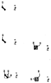
- Figure 8 illustrates the conductive ink 83 and the conductive adhesive 88 as they relate to each other geometrically.
- the improved geometry allows universal orientation of the antenna portions 120 and 121 to the direction of the web and allows efficient interposer 30 insertion regardless of antenna 20 orientation.
- the geometry of components allows for attachment of the interposer chip subcomponent regardless of the orientation of the antenna 20 or similar circuit.
- the antenna gaps 122 may be oriented either parallel or perpendicular to the web direction during printing or insertion.
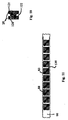
- Figure 9 shows an orientation of a horizontal antenna 20 or similar circuit to the interposer 30
- Figure 10 shows an orientation of a vertical antenna 20 or similar circuit to the interposer 30.
- Figure 11 shows a liner 90, conductive adhesive 88 and conductive ink 83 as an assembly step, which can be used as a reel.
- Figure 1 shows an interposer 30 on a matrix web 40. Different methods and label printing equipment require different configurations of the interposers 30. A leading edge or even a trailing edge of each component can serve as an eye mark 130 for signaling information to production or quality control equipment.
- the method of making a RF type device without the application of heat, comprises the steps of:
- the method of applying the IC mounted on an interposer can be accomplished using a standard press head, which is existing technology for many convertors.
- a standard press head which is existing technology for many convertors.
- numerous interposer-chip subassemblies are prepared for subsequent attachment to circuits to form devices at high line speeds.
- an additional step of detecting defects on the ICs on the interposers can be performed before applying the subassembly to the thin film circuit. If defects are found, the defective IC assembly will be skipped.
Landscapes
- Engineering & Computer Science (AREA)
- Microelectronics & Electronic Packaging (AREA)
- Computer Hardware Design (AREA)
- Physics & Mathematics (AREA)
- General Physics & Mathematics (AREA)
- Theoretical Computer Science (AREA)
- Details Of Aerials (AREA)
- Credit Cards Or The Like (AREA)
- Connections Effected By Soldering, Adhesion, Or Permanent Deformation (AREA)
- Electric Connection Of Electric Components To Printed Circuits (AREA)
- Wire Bonding (AREA)
Applications Claiming Priority (4)
| Application Number | Priority Date | Filing Date | Title |
|---|---|---|---|
| US12584299P | 1999-03-24 | 1999-03-24 | |
| US125842P | 1999-03-24 | ||
| US14948699P | 1999-08-18 | 1999-08-18 | |
| US149486P | 1999-08-18 |
Publications (3)
| Publication Number | Publication Date |
|---|---|
| EP1039543A2 true EP1039543A2 (fr) | 2000-09-27 |
| EP1039543A3 EP1039543A3 (fr) | 2004-01-02 |
| EP1039543B1 EP1039543B1 (fr) | 2014-02-26 |
Family
ID=26824012
Family Applications (1)
| Application Number | Title | Priority Date | Filing Date |
|---|---|---|---|
| EP00302389.2A Expired - Lifetime EP1039543B1 (fr) | 1999-03-24 | 2000-03-23 | Connecteur d'une puce à circuit et methode de connexion de la meme associée |
Country Status (6)
| Country | Link |
|---|---|
| EP (1) | EP1039543B1 (fr) |
| JP (1) | JP4927245B2 (fr) |
| KR (1) | KR20000076944A (fr) |
| CA (1) | CA2302957C (fr) |
| ES (1) | ES2453486T3 (fr) |
| TW (1) | TW457605B (fr) |
Cited By (21)
| Publication number | Priority date | Publication date | Assignee | Title |
|---|---|---|---|---|
| US6867983B2 (en) | 2002-08-07 | 2005-03-15 | Avery Dennison Corporation | Radio frequency identification device and method |
| DE10358423A1 (de) * | 2003-08-26 | 2005-04-07 | Mühlbauer Ag | Modulbrücken für Smart Labels |
| US6940408B2 (en) | 2002-12-31 | 2005-09-06 | Avery Dennison Corporation | RFID device and method of forming |
| WO2006028712A1 (fr) * | 2004-09-01 | 2006-03-16 | Avery Dennison Corporation | Dispositif rfid a coupleur reactif combine |
| WO2006036666A1 (fr) * | 2004-09-22 | 2006-04-06 | Avery Dennison Corporation | Procede et dispositif rapides de placement d'un circuit d'identification radiofrequence |
| US7057562B2 (en) | 2004-03-11 | 2006-06-06 | Avery Dennison Corporation | RFID device with patterned antenna, and method of making |
| EP1693792A1 (fr) | 2002-01-18 | 2006-08-23 | Avery Dennison Corporation | Methode de fabrication d'etiquettes RFID |
| US7120987B2 (en) | 2003-08-05 | 2006-10-17 | Avery Dennison Corporation | Method of making RFID device |
| WO2006116551A1 (fr) * | 2005-04-25 | 2006-11-02 | Avery Dennison Corporation | Procede et dispositif de placement d'un circuit rfid a grande vitesse |
| US7224280B2 (en) | 2002-12-31 | 2007-05-29 | Avery Dennison Corporation | RFID device and method of forming |
| US7292148B2 (en) | 2004-06-18 | 2007-11-06 | Avery Dennison Corporation | Method of variable position strap mounting for RFID transponder |
| US7307527B2 (en) | 2004-07-01 | 2007-12-11 | Avery Dennison Corporation | RFID device preparation system and method |
| US7477194B2 (en) | 2003-04-11 | 2009-01-13 | Avery Dennison Corporation | Conductive pattern and method of making |
| EP2096583A1 (fr) | 2004-03-22 | 2009-09-02 | Avery Dennison Corporation | Procédé de test des dispositifs RFID |
| US7842152B2 (en) | 2005-08-22 | 2010-11-30 | Avery Dennison Corporation | Method of making RFID devices |
| US7930815B2 (en) | 2003-04-11 | 2011-04-26 | Avery Dennison Corporation | Conductive pattern and method of making |
| US8127440B2 (en) | 2006-10-16 | 2012-03-06 | Douglas Joel S | Method of making bondable flexible printed circuit |
| US9652705B1 (en) | 2012-02-21 | 2017-05-16 | Automated Assembly Corporation | RFID tag on flexible substrate arrangement |
| EP3217330A1 (fr) * | 2016-03-07 | 2017-09-13 | Gemalto Sa | Procede de fabrication de module a puce de circuit integre et dispositif comprenant un tel module |
| WO2025163555A1 (fr) | 2024-02-01 | 2025-08-07 | Avery Dennison Retail Information Services Llc | Sangles auto-adhésives pour dispositifs rfid |
| WO2025163552A1 (fr) | 2024-02-01 | 2025-08-07 | Avery Dennison Retail Information Services Llc | Procédé de fixation de sangle humide |
Families Citing this family (14)
| Publication number | Priority date | Publication date | Assignee | Title |
|---|---|---|---|---|
| JP2002288612A (ja) * | 2001-03-27 | 2002-10-04 | Toppan Forms Co Ltd | 荷物用タグの製法 |
| US6606247B2 (en) | 2001-05-31 | 2003-08-12 | Alien Technology Corporation | Multi-feature-size electronic structures |
| JP2003006594A (ja) * | 2001-06-22 | 2003-01-10 | Toppan Forms Co Ltd | 両面テープを用いたrf−idメディアの形成方法 |
| US7253735B2 (en) | 2003-03-24 | 2007-08-07 | Alien Technology Corporation | RFID tags and processes for producing RFID tags |
| US7688206B2 (en) | 2004-11-22 | 2010-03-30 | Alien Technology Corporation | Radio frequency identification (RFID) tag for an item having a conductive layer included or attached |
| CA2493410C (fr) * | 2005-01-20 | 2016-09-27 | Intelligent Devices Inc. | Processus d'assemblage, de production et d'assurance qualite relatifs a des etiquettes de surveillance de conformite electronique (ecm) |
| JP2006260205A (ja) | 2005-03-17 | 2006-09-28 | Fujitsu Ltd | Rfidタグ、モジュール部品、およびrfidタグ製造方法 |
| US8067253B2 (en) | 2005-12-21 | 2011-11-29 | Avery Dennison Corporation | Electrical device and method of manufacturing electrical devices using film embossing techniques to embed integrated circuits into film |
| US7555826B2 (en) | 2005-12-22 | 2009-07-07 | Avery Dennison Corporation | Method of manufacturing RFID devices |
| JP5034371B2 (ja) | 2006-02-10 | 2012-09-26 | 富士通株式会社 | Rfidタグの製造方法およびrfidタグ |
| KR100862450B1 (ko) * | 2007-05-18 | 2008-10-08 | 삼성전기주식회사 | 라디오 모듈 및 제조방법 |
| KR101539125B1 (ko) * | 2007-10-10 | 2015-07-23 | 코비오 인코포레이티드 | 인쇄 집적 회로소자를 포함하는 무선 장치 및 이의 제조 및 사용 방법 |
| US20220230038A1 (en) * | 2019-04-22 | 2022-07-21 | Avery Dennison Retail Information Services Llc | Self-adhesive straps for rfid devices |
| US11145966B2 (en) * | 2019-08-28 | 2021-10-12 | Pctel, Inc. | Over-molded thin film antenna device |
Family Cites Families (18)
| Publication number | Priority date | Publication date | Assignee | Title |
|---|---|---|---|---|
| NO146835C (no) * | 1977-12-09 | 1982-12-15 | Lintech Instr Ltd | Passivt transponder-element. |
| NL7713758A (nl) * | 1977-12-13 | 1979-06-15 | Philips Nv | Halfgeleiderinrichting. |
| CA1218954A (fr) * | 1982-02-25 | 1987-03-10 | David L. Sieverding | Colle de contact elastomere hydrophile |
| US4977441A (en) * | 1985-12-25 | 1990-12-11 | Hitachi, Ltd. | Semiconductor device and tape carrier |
| US4766670A (en) * | 1987-02-02 | 1988-08-30 | International Business Machines Corporation | Full panel electronic packaging structure and method of making same |
| JP2758030B2 (ja) * | 1988-07-04 | 1998-05-25 | ソニー株式会社 | 薄型電子機器とその製造方法 |
| JP2627320B2 (ja) * | 1988-10-18 | 1997-07-02 | 三洋電機株式会社 | スペクトラム拡散信号復調回路 |
| JP2811713B2 (ja) * | 1989-02-13 | 1998-10-15 | ソニー株式会社 | 情報カード |
| US5776278A (en) * | 1992-06-17 | 1998-07-07 | Micron Communications, Inc. | Method of manufacturing an enclosed transceiver |
| US5491303A (en) * | 1994-03-21 | 1996-02-13 | Motorola, Inc. | Surface mount interposer |
| US5528222A (en) * | 1994-09-09 | 1996-06-18 | International Business Machines Corporation | Radio frequency circuit and memory in thin flexible package |
| US5682143A (en) * | 1994-09-09 | 1997-10-28 | International Business Machines Corporation | Radio frequency identification tag |
| JPH0890966A (ja) * | 1994-09-22 | 1996-04-09 | Rohm Co Ltd | 非接触型icカードの構造 |
| DE19716342C2 (de) * | 1997-04-18 | 1999-02-25 | Pav Card Gmbh | Verfahren zur Herstellung einer Chipkarte |
| JPH115384A (ja) * | 1997-06-18 | 1999-01-12 | Hitachi Maxell Ltd | 薄型電子機器ならびにその製造方法 |
| JPH1159036A (ja) * | 1997-08-21 | 1999-03-02 | Hitachi Maxell Ltd | 非接触icカード及びその製造方法 |
| BR9811446A (pt) * | 1997-09-11 | 2000-08-22 | Precision Dynamics Corp | Dispositivo de identificação de rádio frequência laminado |
| US6107920A (en) * | 1998-06-09 | 2000-08-22 | Motorola, Inc. | Radio frequency identification tag having an article integrated antenna |
-
2000
- 2000-03-23 ES ES00302389.2T patent/ES2453486T3/es not_active Expired - Lifetime
- 2000-03-23 CA CA002302957A patent/CA2302957C/fr not_active Expired - Lifetime
- 2000-03-23 EP EP00302389.2A patent/EP1039543B1/fr not_active Expired - Lifetime
- 2000-03-23 TW TW089105335A patent/TW457605B/zh not_active IP Right Cessation
- 2000-03-24 KR KR1020000015007A patent/KR20000076944A/ko not_active Ceased
- 2000-03-24 JP JP2000088549A patent/JP4927245B2/ja not_active Expired - Fee Related
Cited By (39)
| Publication number | Priority date | Publication date | Assignee | Title |
|---|---|---|---|---|
| EP1693792A1 (fr) | 2002-01-18 | 2006-08-23 | Avery Dennison Corporation | Methode de fabrication d'etiquettes RFID |
| EP1470528B2 (fr) † | 2002-01-18 | 2016-10-05 | Avery Dennison Corporation | Technique de production d'etiquettes rfid |
| EP2306372A1 (fr) * | 2002-01-18 | 2011-04-06 | Avery Dennison Corporation | Méthode de fabrication d'étiquettes RFID |
| US7361251B2 (en) | 2002-01-18 | 2008-04-22 | Avery Dennison Corporation | RFID label technique |
| EP1693792B1 (fr) * | 2002-01-18 | 2015-08-12 | Avery Dennison Corporation | Methode de fabrication d'etiquettes RFID |
| US8246773B2 (en) | 2002-01-18 | 2012-08-21 | Avery Dennison Corporation | RFID label technique |
| US6867983B2 (en) | 2002-08-07 | 2005-03-15 | Avery Dennison Corporation | Radio frequency identification device and method |
| US7102520B2 (en) | 2002-12-31 | 2006-09-05 | Avery Dennison Corporation | RFID device and method of forming |
| US8072333B2 (en) | 2002-12-31 | 2011-12-06 | Avery Dennison Corporation | RFID device and method of forming |
| US7224280B2 (en) | 2002-12-31 | 2007-05-29 | Avery Dennison Corporation | RFID device and method of forming |
| US6940408B2 (en) | 2002-12-31 | 2005-09-06 | Avery Dennison Corporation | RFID device and method of forming |
| US8769805B2 (en) | 2003-04-11 | 2014-07-08 | Avery Dennison Corporation | Method of making conductive pattern |
| US9159018B2 (en) | 2003-04-11 | 2015-10-13 | Avery Dennison Corporation | Method of making conductive patterns |
| US7930815B2 (en) | 2003-04-11 | 2011-04-26 | Avery Dennison Corporation | Conductive pattern and method of making |
| US7477194B2 (en) | 2003-04-11 | 2009-01-13 | Avery Dennison Corporation | Conductive pattern and method of making |
| US7120987B2 (en) | 2003-08-05 | 2006-10-17 | Avery Dennison Corporation | Method of making RFID device |
| US7333061B2 (en) | 2003-08-05 | 2008-02-19 | Avery Dennison Corporation | RFID device and method of making |
| DE10358423B4 (de) * | 2003-08-26 | 2006-09-21 | Mühlbauer Ag | Modulbrücken für Smart Labels |
| DE10358423A1 (de) * | 2003-08-26 | 2005-04-07 | Mühlbauer Ag | Modulbrücken für Smart Labels |
| US7057562B2 (en) | 2004-03-11 | 2006-06-06 | Avery Dennison Corporation | RFID device with patterned antenna, and method of making |
| EP2096583A1 (fr) | 2004-03-22 | 2009-09-02 | Avery Dennison Corporation | Procédé de test des dispositifs RFID |
| EP2096584A1 (fr) | 2004-03-22 | 2009-09-02 | Avery Dennison Corporation | Procédé de test des dispositifs RFID |
| US7292148B2 (en) | 2004-06-18 | 2007-11-06 | Avery Dennison Corporation | Method of variable position strap mounting for RFID transponder |
| US7307527B2 (en) | 2004-07-01 | 2007-12-11 | Avery Dennison Corporation | RFID device preparation system and method |
| WO2006028712A1 (fr) * | 2004-09-01 | 2006-03-16 | Avery Dennison Corporation | Dispositif rfid a coupleur reactif combine |
| US7158033B2 (en) | 2004-09-01 | 2007-01-02 | Avery Dennison Corporation | RFID device with combined reactive coupler |
| WO2006036666A1 (fr) * | 2004-09-22 | 2006-04-06 | Avery Dennison Corporation | Procede et dispositif rapides de placement d'un circuit d'identification radiofrequence |
| CN101069196B (zh) * | 2004-09-22 | 2010-06-16 | 艾利丹尼森公司 | 高速rfid电路放置方法与器件 |
| CN101496038B (zh) * | 2005-04-25 | 2013-04-03 | 艾利丹尼森公司 | 高速放置射频识别电路的方法和装置 |
| US8531297B2 (en) | 2005-04-25 | 2013-09-10 | Avery Dennison Corporation | High-speed RFID circuit placement method and device |
| WO2006116551A1 (fr) * | 2005-04-25 | 2006-11-02 | Avery Dennison Corporation | Procede et dispositif de placement d'un circuit rfid a grande vitesse |
| US7623034B2 (en) | 2005-04-25 | 2009-11-24 | Avery Dennison Corporation | High-speed RFID circuit placement method and device |
| US7842152B2 (en) | 2005-08-22 | 2010-11-30 | Avery Dennison Corporation | Method of making RFID devices |
| US8127440B2 (en) | 2006-10-16 | 2012-03-06 | Douglas Joel S | Method of making bondable flexible printed circuit |
| US9652705B1 (en) | 2012-02-21 | 2017-05-16 | Automated Assembly Corporation | RFID tag on flexible substrate arrangement |
| EP3217330A1 (fr) * | 2016-03-07 | 2017-09-13 | Gemalto Sa | Procede de fabrication de module a puce de circuit integre et dispositif comprenant un tel module |
| WO2017153353A1 (fr) * | 2016-03-07 | 2017-09-14 | Gemalto Sa | Procede de fabrication de module a puce de circuit integre et dispositif comprenant un tel module |
| WO2025163555A1 (fr) | 2024-02-01 | 2025-08-07 | Avery Dennison Retail Information Services Llc | Sangles auto-adhésives pour dispositifs rfid |
| WO2025163552A1 (fr) | 2024-02-01 | 2025-08-07 | Avery Dennison Retail Information Services Llc | Procédé de fixation de sangle humide |
Also Published As
| Publication number | Publication date |
|---|---|
| CA2302957C (fr) | 2009-06-30 |
| TW457605B (en) | 2001-10-01 |
| JP4927245B2 (ja) | 2012-05-09 |
| EP1039543A3 (fr) | 2004-01-02 |
| JP2000311233A (ja) | 2000-11-07 |
| EP1039543B1 (fr) | 2014-02-26 |
| CA2302957A1 (fr) | 2000-09-24 |
| ES2453486T3 (es) | 2014-04-07 |
| KR20000076944A (ko) | 2000-12-26 |
Similar Documents
| Publication | Publication Date | Title |
|---|---|---|
| US7300863B2 (en) | Circuit chip connector and method of connecting a circuit chip | |
| CA2302957C (fr) | Connecteur de puce de circuit et methode de connexion d'une puce de circuit | |
| EP1399881B1 (fr) | Etiquette intelligente et reseau d'une etiquette intelligente | |
| US5972156A (en) | Method of making a radio frequency identification tag | |
| KR100555337B1 (ko) | 테이프 캐리어 | |
| EP0821406B1 (fr) | Un circuit intégré sur un substrat ultra-flexible et un procédé pour relier par fils un circuit intégré à un substrat ultra-flexible | |
| US7551141B1 (en) | RFID strap capacitively coupled and method of making same | |
| US8162231B2 (en) | Noncontact IC tag label and method of manufacturing the same | |
| US20020020491A1 (en) | High speed flip chip assembly process | |
| US20110017832A1 (en) | Rfid tag | |
| KR20040075095A (ko) | 알에프아이디 라벨 기술 | |
| CN209766617U (zh) | 一种天线与芯片平面交叉的射频谐振腔总成 | |
| JP2000235635A (ja) | コンデンサ内蔵非接触型icカードとその製造方法 | |
| JP4353181B2 (ja) | 電子装置の製造方法 | |
| AU2005234764B9 (en) | Method of forming RFID circuit assembly | |
| CN101334853A (zh) | 一种电子标签的封装方法 | |
| US7229018B2 (en) | Manufacture of RFID tags and intermediate products therefor | |
| US7616171B2 (en) | Connecting part of conductor pattern and conductor patterns-connected structure | |
| HK1027667A (en) | Circuit chip connector and method of connecting a circuit chip | |
| US7431218B2 (en) | RFID tag, module component, and RFID tag fabrication method | |
| JP4319726B2 (ja) | 非接触型icカードの製造方法 | |
| JP2001203296A (ja) | Icカード用icチップ実装基板 | |
| KR20070055606A (ko) | 전기 또는 전자기계 장치의 마이크로 패키징 방법 및마이크로 패키지 | |
| CN121145908A (zh) | Rfid标签及制备方法、使用方法、商品、商品外包装 | |
| JPH11345301A (ja) | 非接触式icシート及びこの非接触式icシートの製造方法 |
Legal Events
| Date | Code | Title | Description |
|---|---|---|---|
| PUAI | Public reference made under article 153(3) epc to a published international application that has entered the european phase |
Free format text: ORIGINAL CODE: 0009012 |
|
| AK | Designated contracting states |
Kind code of ref document: A2 Designated state(s): AT BE CH CY DE DK ES FI FR GB GR IE IT LI LU MC NL PT SE |
|
| AX | Request for extension of the european patent |
Free format text: AL;LT;LV;MK;RO;SI |
|
| RAP1 | Party data changed (applicant data changed or rights of an application transferred) |
Owner name: MOTOROLA, INC. |
|
| RIN1 | Information on inventor provided before grant (corrected) |
Inventor name: PENNAZ, THOMAS J. Inventor name: EBERHARDT, NOEL H. |
|
| PUAL | Search report despatched |
Free format text: ORIGINAL CODE: 0009013 |
|
| AK | Designated contracting states |
Kind code of ref document: A3 Designated state(s): AT BE CH CY DE DK ES FI FR GB GR IE IT LI LU MC NL PT SE |
|
| AX | Request for extension of the european patent |
Extension state: AL LT LV MK RO SI |
|
| RIC1 | Information provided on ipc code assigned before grant |
Ipc: 7G 06K 19/077 B Ipc: 7H 01L 23/498 A Ipc: 7H 01L 21/60 B |
|
| 17P | Request for examination filed |
Effective date: 20040625 |
|
| AKX | Designation fees paid |
Designated state(s): AT BE CH CY DE DK ES FI FR GB GR IE IT LI LU MC NL PT SE |
|
| R17P | Request for examination filed (corrected) |
Effective date: 20040625 |
|
| RBV | Designated contracting states (corrected) |
Designated state(s): AT BE CH CY DE DK ES FI FR GB GR IE IT LI LU MC NL PT SE |
|
| 17Q | First examination report despatched |
Effective date: 20050512 |
|
| RAP1 | Party data changed (applicant data changed or rights of an application transferred) |
Owner name: MOTOROLA SOLUTIONS, INC. |
|
| GRAP | Despatch of communication of intention to grant a patent |
Free format text: ORIGINAL CODE: EPIDOSNIGR1 |
|
| INTG | Intention to grant announced |
Effective date: 20130917 |
|
| GRAS | Grant fee paid |
Free format text: ORIGINAL CODE: EPIDOSNIGR3 |
|
| GRAA | (expected) grant |
Free format text: ORIGINAL CODE: 0009210 |
|
| AK | Designated contracting states |
Kind code of ref document: B1 Designated state(s): AT BE CH CY DE DK ES FI FR GB GR IE IT LI LU MC NL PT SE |
|
| REG | Reference to a national code |
Ref country code: GB Ref legal event code: FG4D Ref country code: DE Ref legal event code: R081 Ref document number: 60048440 Country of ref document: DE Owner name: MOTOROLA SOLUTIONS, INC., CHICAGO, US Free format text: FORMER OWNER: MORGAN ADHESIVES CO., STOW, OHIO, US |
|
| REG | Reference to a national code |
Ref country code: CH Ref legal event code: EP |
|
| REG | Reference to a national code |
Ref country code: AT Ref legal event code: REF Ref document number: 654028 Country of ref document: AT Kind code of ref document: T Effective date: 20140315 |
|
| REG | Reference to a national code |
Ref country code: DE Ref legal event code: R096 Ref document number: 60048440 Country of ref document: DE Effective date: 20140403 |
|
| REG | Reference to a national code |
Ref country code: ES Ref legal event code: FG2A Ref document number: 2453486 Country of ref document: ES Kind code of ref document: T3 Effective date: 20140407 |
|
| REG | Reference to a national code |
Ref country code: IE Ref legal event code: FG4D |
|
| REG | Reference to a national code |
Ref country code: NL Ref legal event code: T3 |
|
| REG | Reference to a national code |
Ref country code: AT Ref legal event code: MK05 Ref document number: 654028 Country of ref document: AT Kind code of ref document: T Effective date: 20140226 |
|
| PG25 | Lapsed in a contracting state [announced via postgrant information from national office to epo] |
Ref country code: AT Free format text: LAPSE BECAUSE OF FAILURE TO SUBMIT A TRANSLATION OF THE DESCRIPTION OR TO PAY THE FEE WITHIN THE PRESCRIBED TIME-LIMIT Effective date: 20140226 Ref country code: FI Free format text: LAPSE BECAUSE OF FAILURE TO SUBMIT A TRANSLATION OF THE DESCRIPTION OR TO PAY THE FEE WITHIN THE PRESCRIBED TIME-LIMIT Effective date: 20140226 Ref country code: CY Free format text: LAPSE BECAUSE OF FAILURE TO SUBMIT A TRANSLATION OF THE DESCRIPTION OR TO PAY THE FEE WITHIN THE PRESCRIBED TIME-LIMIT Effective date: 20140226 Ref country code: SE Free format text: LAPSE BECAUSE OF FAILURE TO SUBMIT A TRANSLATION OF THE DESCRIPTION OR TO PAY THE FEE WITHIN THE PRESCRIBED TIME-LIMIT Effective date: 20140226 Ref country code: PT Free format text: LAPSE BECAUSE OF FAILURE TO SUBMIT A TRANSLATION OF THE DESCRIPTION OR TO PAY THE FEE WITHIN THE PRESCRIBED TIME-LIMIT Effective date: 20140626 |
|
| PG25 | Lapsed in a contracting state [announced via postgrant information from national office to epo] |
Ref country code: DK Free format text: LAPSE BECAUSE OF FAILURE TO SUBMIT A TRANSLATION OF THE DESCRIPTION OR TO PAY THE FEE WITHIN THE PRESCRIBED TIME-LIMIT Effective date: 20140226 |
|
| REG | Reference to a national code |
Ref country code: CH Ref legal event code: PL |
|
| REG | Reference to a national code |
Ref country code: DE Ref legal event code: R097 Ref document number: 60048440 Country of ref document: DE |
|
| PG25 | Lapsed in a contracting state [announced via postgrant information from national office to epo] |
Ref country code: MC Free format text: LAPSE BECAUSE OF FAILURE TO SUBMIT A TRANSLATION OF THE DESCRIPTION OR TO PAY THE FEE WITHIN THE PRESCRIBED TIME-LIMIT Effective date: 20140226 |
|
| REG | Reference to a national code |
Ref country code: IE Ref legal event code: MM4A |
|
| PLBE | No opposition filed within time limit |
Free format text: ORIGINAL CODE: 0009261 |
|
| STAA | Information on the status of an ep patent application or granted ep patent |
Free format text: STATUS: NO OPPOSITION FILED WITHIN TIME LIMIT |
|
| PG25 | Lapsed in a contracting state [announced via postgrant information from national office to epo] |
Ref country code: CH Free format text: LAPSE BECAUSE OF NON-PAYMENT OF DUE FEES Effective date: 20140331 Ref country code: LI Free format text: LAPSE BECAUSE OF NON-PAYMENT OF DUE FEES Effective date: 20140331 Ref country code: IE Free format text: LAPSE BECAUSE OF NON-PAYMENT OF DUE FEES Effective date: 20140323 |
|
| 26N | No opposition filed |
Effective date: 20141127 |
|
| REG | Reference to a national code |
Ref country code: DE Ref legal event code: R097 Ref document number: 60048440 Country of ref document: DE Effective date: 20141127 |
|
| PG25 | Lapsed in a contracting state [announced via postgrant information from national office to epo] |
Ref country code: IT Free format text: LAPSE BECAUSE OF FAILURE TO SUBMIT A TRANSLATION OF THE DESCRIPTION OR TO PAY THE FEE WITHIN THE PRESCRIBED TIME-LIMIT Effective date: 20140226 |
|
| REG | Reference to a national code |
Ref country code: FR Ref legal event code: PLFP Year of fee payment: 17 |
|
| PG25 | Lapsed in a contracting state [announced via postgrant information from national office to epo] |
Ref country code: GR Free format text: LAPSE BECAUSE OF FAILURE TO SUBMIT A TRANSLATION OF THE DESCRIPTION OR TO PAY THE FEE WITHIN THE PRESCRIBED TIME-LIMIT Effective date: 20140527 |
|
| PG25 | Lapsed in a contracting state [announced via postgrant information from national office to epo] |
Ref country code: LU Free format text: LAPSE BECAUSE OF NON-PAYMENT OF DUE FEES Effective date: 20140323 |
|
| REG | Reference to a national code |
Ref country code: DE Ref legal event code: R082 Ref document number: 60048440 Country of ref document: DE Representative=s name: SCHUMACHER & WILLSAU PATENTANWALTSGESELLSCHAFT, DE Ref country code: DE Ref legal event code: R081 Ref document number: 60048440 Country of ref document: DE Owner name: MOTOROLA SOLUTIONS, INC., CHICAGO, US Free format text: FORMER OWNER: MOTOROLA SOLUTIONS, INC., SCHAUMBURG, ILL., US |
|
| REG | Reference to a national code |
Ref country code: FR Ref legal event code: PLFP Year of fee payment: 18 |
|
| REG | Reference to a national code |
Ref country code: FR Ref legal event code: CA Effective date: 20180105 |
|
| REG | Reference to a national code |
Ref country code: FR Ref legal event code: PLFP Year of fee payment: 19 |
|
| PGFP | Annual fee paid to national office [announced via postgrant information from national office to epo] |
Ref country code: NL Payment date: 20180323 Year of fee payment: 19 |
|
| PGFP | Annual fee paid to national office [announced via postgrant information from national office to epo] |
Ref country code: BE Payment date: 20180323 Year of fee payment: 19 Ref country code: FR Payment date: 20180329 Year of fee payment: 19 |
|
| PGFP | Annual fee paid to national office [announced via postgrant information from national office to epo] |
Ref country code: ES Payment date: 20180423 Year of fee payment: 19 |
|
| PGFP | Annual fee paid to national office [announced via postgrant information from national office to epo] |
Ref country code: GB Payment date: 20190327 Year of fee payment: 20 |
|
| PGFP | Annual fee paid to national office [announced via postgrant information from national office to epo] |
Ref country code: DE Payment date: 20190528 Year of fee payment: 20 |
|
| REG | Reference to a national code |
Ref country code: NL Ref legal event code: MM Effective date: 20190401 |
|
| REG | Reference to a national code |
Ref country code: BE Ref legal event code: MM Effective date: 20190331 |
|
| PG25 | Lapsed in a contracting state [announced via postgrant information from national office to epo] |
Ref country code: NL Free format text: LAPSE BECAUSE OF NON-PAYMENT OF DUE FEES Effective date: 20190401 |
|
| PG25 | Lapsed in a contracting state [announced via postgrant information from national office to epo] |
Ref country code: FR Free format text: LAPSE BECAUSE OF NON-PAYMENT OF DUE FEES Effective date: 20190331 Ref country code: BE Free format text: LAPSE BECAUSE OF NON-PAYMENT OF DUE FEES Effective date: 20190331 |
|
| REG | Reference to a national code |
Ref country code: DE Ref legal event code: R071 Ref document number: 60048440 Country of ref document: DE |
|
| REG | Reference to a national code |
Ref country code: GB Ref legal event code: PE20 Expiry date: 20200322 |
|
| PG25 | Lapsed in a contracting state [announced via postgrant information from national office to epo] |
Ref country code: GB Free format text: LAPSE BECAUSE OF EXPIRATION OF PROTECTION Effective date: 20200322 |
|
| REG | Reference to a national code |
Ref country code: ES Ref legal event code: FD2A Effective date: 20200728 |
|
| PG25 | Lapsed in a contracting state [announced via postgrant information from national office to epo] |
Ref country code: ES Free format text: LAPSE BECAUSE OF NON-PAYMENT OF DUE FEES Effective date: 20190324 |