EP1040574B1 - Künstliche leitung - Google Patents
Künstliche leitung Download PDFInfo
- Publication number
- EP1040574B1 EP1040574B1 EP98954902A EP98954902A EP1040574B1 EP 1040574 B1 EP1040574 B1 EP 1040574B1 EP 98954902 A EP98954902 A EP 98954902A EP 98954902 A EP98954902 A EP 98954902A EP 1040574 B1 EP1040574 B1 EP 1040574B1
- Authority
- EP
- European Patent Office
- Prior art keywords
- artificial line
- artificial
- line
- switching element
- frequency
- Prior art date
- Legal status (The legal status is an assumption and is not a legal conclusion. Google has not performed a legal analysis and makes no representation as to the accuracy of the status listed.)
- Expired - Lifetime
Links
Images


Classifications
-
- H—ELECTRICITY
- H03—ELECTRONIC CIRCUITRY
- H03H—IMPEDANCE NETWORKS, e.g. RESONANT CIRCUITS; RESONATORS
- H03H11/00—Networks using active elements
- H03H11/02—Multiple-port networks
- H03H11/26—Time-delay networks
- H03H11/265—Time-delay networks with adjustable delay
Definitions
- the present invention relates to an artificial line, i.e. an artificial electric line, and specifically an artificial line having a constant group delay in a wide frequency range (octave bandwidths)
- an artificial line i.e. an artificial electric line
- an artificial line having a constant group delay in a wide frequency range e.g. from US 4885562.
- the invention originates from delay lines for radar applications and will partly be described starting from this.
- the invention can be applied in other contexts where an artificial line having the achieved properties can be used. Therefore the inventor aims at protecting the artificial line by a patent, based on its construction and its properties and independently of the place where it is used.
- phased array antennas Since such antennas may have hundreds of modules, monolithic integrated microwaves circuits (MMIC) are necessary to minimise size and weight.
- MMIC monolithic integrated microwaves circuits
- Most prior-art microwave systems with phased array antennas are provided with binary control devices. In large installations, a great number of control wires will be involved since each element must be controlled individually. If an analog control device could be used, much would be gained since only one control wire or a few control wires would be required.
- phase shifters cannot be used since they cause a change in the beam direction, phase squinting, and distortion of the pulses, pulse stretching. Therefore the invention instead uses a special embodiment of a controllable delay element since such elements allow frequency-independent beam steering.
- Prior-art controllable delay elements are digital, which causes losses. Besides they are expensive.
- Fig. 1 shows a prior-art binary 4-bit delay element using single-pole double-throw switches (SPDT).
- SPDT single-pole double-throw switches
- Single-pole double-throw switches have considerable losses, which means that the prior-art delay element all in all exhibits great losses. If in Fig. 1 the delay ⁇ t is 8 ps, the maximum delay will be 120 ps.
- the present invention solves the above problem by providing an artificial line with controllable delay and low losses and at a, relatively seen, low cost by being designed in the manner that appears from the independent claim.
- Advantageous embodiments of the invention are defined in the remaining claims.
- the invention concerns basically an artificial line which in a first state has the desired properties in respect of constant group delay in a wide frequency range.
- the artificial line can then be accomplished as a continuously tunable artificial line or as a self-switched artificial line.
- Fig. 2 illustrates how, in one embodiment, it would be possible to build a composed artificial line which can delay signals by a total of 120 ps, the same as in the previous case of the prior-art artificial line.
- a tunable artificial line A as well as self-switched artificial lines B.
- the continuously tunable artificial line has, in dependence on a control signal, a delay of up to about 20 ps.
- five self-switched artificial lines are cascade-coupled to this artificial line.
- the self-switched artificial line can take two distinct states. In one state, it has a small delay, and in the other a large delay, in the example at issue about 20 ps.
- the self-switched artificial lines can be controlled by a single control wire, which means a considerable simplification.
- Both types of artificial line are based on an all-pass network with a frequency-independent mirror impedance (constant-R all-pass network). In the tunable case, it is more correct to speak of essentially frequency-independent mirror impedance (quasi constant-R ).
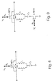
- Fig. 3a illustrates a known all-pass network. It consists of a bridged T-section consisting of two mutually coupled inductors of equal value L, which form the two arms, a capacitor C 2 to earth, forming the vertical arm, and a capacitor C 1 coupled over the inductors. Under specific conditions, this network becomes an all-pass network having a constant input impedance which is independent of frequency.
- the transfer function has a low-pass character.
- the normalised circuit elements can now be expressed as functions of a and b. Insertion of the expressions for a and b in (12) results in
- the transfer phase must have a linear frequency response.
- the group delay GD ( ⁇ ) must be constant with frequency.
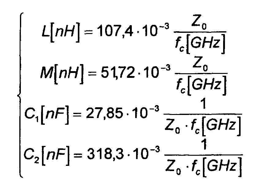
- the self-switched artificial line can take two states. In one state, the circuit has component values according to equation (18), which results in a large delay. In the second state, the capacitor C 1 is short-circuited, which gives a short delay.
- the capacitor C 1 can be implemented as a metal-insulator metal (MIM) capacitor in an MMIC design.
- MIM metal-insulator metal
- the capacitor C 1 is exchanged for a first switching element which can be described as a small resistor in a first state (on-state) and a capacitor in a second state (off-state), e.g. a PIN diode, a bipolar transistor or a "switch-FET".
- the transistor is biased so as to be fully depleted,
- the transistor then corresponds to a capacitor. If the transistor parameters are selected such that the capacitance of the transistor is C 1 , the circuit obtains, according to the derivation which results in equation (18), a group delay which is independent of the frequency in a wide frequency range.
- the shunt capacitor C 2 is normally not small enough to give a high impedance to the line when the first field effect transistor FET 1 is in the first state. This results in a deterioration of the scattering properties, especially at high frequencies.
- a solution to this is to connect a second switching element, of a type similar to the first one, in series with the capacitor C 2 . This second switching element is driven complementarily with the first, i.e. when the first is conductive, the second is fully depleted and vice versa. In this way, the line becomes shunted by a high impedance compared with C 2 only.
- Fig. 8 shows a variant of this advantageous embodiment of the invention with a second field effect transistor, FET 2, optimised to take, in dependence on its control voltage, two distinct states, as the second switching element.
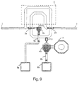
- Figs 9 and 10 Two examples of a concrete layout for a self-switched artificial line in a planar monolithic circuit technique are shown in Figs 9 and 10.
- the cut-off frequency is selected to be 18 GHz and the characteristic impedance to be 50 ⁇ .
- the desired element values are the same in the two examples.
- the embodiments result in different group delay owing to the different geometric design of the circuits, which will be described below.
- the embodiments in the Figures are drawn according to scale for accomplishment on a 100 ⁇ m-thick GaAs substrate having the permitivity 12.8.
- Fig. 9 shows an embodiment in which the largest possible difference in group delay between the two states of the circuit is desired.
- the circuit has an input 1 and an output 2.
- the inductances and the mutual inductance are realised as coupled microstrip lines 3.
- the bias of FET 1 and FET 2 is applied to the bonding pads 8a and 8b, respectively, and is supplied to the gate via the respective resistors 9a and 9b which are here designed as doped channels in the substrate with controlled resistivity
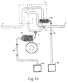
- Fig. 10 shows an embodiment in which a smaller difference in group delay between the two states of the circuit is desired.
- the circuit has an input 1 and an output 2.
- the inductances and the mutual inductance are realised as coupled microstrip lines 3.
- only one insulating crossover 5 is necessary.
- the bias of FET 1 and FET 2 is applied to the bond plates 8a and 8b, respectively, and is supplied to gate via the respective resistors 9a and 9b, which are here designed as doped channels in the substrate with controlled resistivity.
- Fig. 11 shows an example of cascade-coupled self-switched artificial lines.
- the continuously tunable group delay is achieved by the capacitors C 1 and C 2 in the two-port network according to Fig. 3a being replaced by varactors, see Fig. 13.
- the varactors are selected such that their capacitances C 1 and C 2 are variable and follow the curves in Fig. 5 in the range for the desired variation of the group delay.
- the inductances L and the mutual inductance M will not follow the relation exactly, and therefore the properties of the circuit are slightly deteriorated.
- the deterioration of the input and output impedance is normally acceptable. It is in this case more correct to speak about an essentially frequency-independent mirror impedance (quasi constant-R ).
- Fig. 15 illustrates an example of a layout for a tunable artificial line.
- the circuit has an input 1 and an output 2.
- the inductances and the mutual inductance are realised as coupled microstrip lines 3.
- the voltage-controlled capacitance C V 1 is designed as a varactor consisting of a field effect transistor 4a where the drain and source are interconnected and the bias for tuning is applied to its gate.
- the voltage-controlled capacitance C V 2 is also designed as a varactor 4b composed in the same manner as the first-mentioned varactor 4a.
- the drain and source of this varactor 4b are connected to the ground plane of the circuit with a via hole 7.
- the design uses an insulating crossover 5.
- the voltage for tuning of C V 1 and C V 2 is applied to the bonding pads 8a and 8b respectively and is supplied to the gate via the respective resistors 9a and 9b which are here designed as doped channels in the substrate with controlled resistivity.
- Two MIM capacitors 10a and 10b have been introduced for the varactors to be biased.
Landscapes
- Networks Using Active Elements (AREA)
- Filters And Equalizers (AREA)
- Cable Transmission Systems, Equalization Of Radio And Reduction Of Echo (AREA)
- External Artificial Organs (AREA)
- Prostheses (AREA)
- Microwave Amplifiers (AREA)
Claims (11)
- Künstliche Leitung in Form eines Netzwerks mit zwei Anschlüssen mit einer im Wesentlichen frequenzunabhängigen Spiegelimpedanz, wobei die künstliche Leitung in einem ersten Zustand zwei identische Induktoren der Stärke L aufweist, die in Reihe geschaltet sind und eine gegenseitige Induktivität M aufweisen, weiter einen Kondensator der Stärke C1, der parallel zu den beiden Induktoren geschaltet ist, sowie einen Nebenschlusskondensator C2, der mit Masse verbunden ist, dadurch gekennzeichnet, dass die künstliche Leitung dazu ausgelegt ist, die selbe Gruppenverzögerung durch die Elementwerte als eine Funktion der Grenzfrequenz fc und der charakteristischen Impedanz Z0 anzugeben, welche gemäß folgenden Gleichungen ausgewählt werden:
- Künstliche Leitung nach Anspruch 1, dadurch gekennzeichnet, dass die künstliche Leitung eine selbstgeschaltete künstliche Leitung ist und einen zweiten Zustand mit kurzer Verzögerung annehmen kann, indem der Kondensator C1 durch einen Kurzschluss ersetzt wird.
- Künstliche Leitung nach Anspruch 2, dadurch gekennzeichnet, dass der Kondensator C1 als ein erstes Schaltelement (FET 1, 4a) ausgebildet ist, das dazu ausgelegt ist, in Abhängigkeit von seiner Steuerspannung zwei verschiedene Zustände anzunehmen, einen ersten, einer Kapazität des Wertes C1 entsprechenden, der der künstlichen Leitung eine lange Verzögerung verleiht, und einen zweiten, einem Kurzschluss mit geringer Impedanz entsprechenden Zustand, der der künstlichen Leitung eine kurze Verzögerung verleiht.
- Künstliche Leitung nach Anspruch 3, dadurch gekennzeichnet, dass das erste Schaltelement (FET 1, 4a) als ein erster Feldeffekttransistor ausgebildet ist.
- Künstliche Leitung nach Anspruch 3 oder 4, dadurch gekennzeichnet, dass ein zweites Schaltelement (FET 2, 4b) mit den selben Eigenschaften wie das erste Schaltelement (FET 1, 4a) in Reihe mit dem Kondensator C2 geschaltet ist, wobei das zweite Schaltelement komplementär zu dem ersten Schaltelement angesteuert wird.
- Künstliche Leitung nach einem der Ansprüche 3 bis 5, dadurch gekennzeichnet, dass sie in einem Verfahren für planar-monolithische Schaltkreise gefertigt ist, wobei die Induktoren und die gemeinsame Induktivität als gekoppelte Mikrostrip-Leitungen (3) ausgebildet sind, und der Kurzschluss, der im zweiten Zustand des Schaltkreises gebildet wird, das erste Schaltelement (FET 1, 4a) und zwei isolierende Überkreuzungsstellen (5a, 5b) der Mikrostrip-Leitungen aufweist und den kürzestmöglichen Übertragungspfad zwischen Eingang (1) und Ausgang (2) bildet.
- Künstliche Leitung nach einem der Ansprüche 3 bis 5, dadurch gekennzeichnet, dass sie in einem Verfahren für planar-monolithische Schaltkreise gefertigt ist, wobei die Induktoren und die gemeinsame Induktivität als gekoppelte Mikrostrip-Leitungen (3) ausgebildet sind, und der Kurzschluss, der im zweiten Zustand des Schaltkreises gebildet wird, das erste Schaltelement (FET 1, 4a), eine der gekoppelten Mikrostrip-Leitungen (3b) und eine isolierende Überkreuzungsstelle (5) einer Mikrostrip-Leitung aufweist.
- Zusammengesetzte künstliche Leitung, welche eine Vielzahl künstlicher Leitungen nach einem der Ansprüche 2 bis 5 aufweist, die als Kaskade geschaltet sind, wobei eine Steuerspannung für die gesamte zusammengesetzte künstliche Leitung an die unterschiedlichen künstlichen Leitungen in Reihe über Zwischenimpedanzen (R) derart angelegt wird, dass jeweilige künstliche Leitungen ihren Zustand nacheinander ändern, wenn die Steuerspannung ansteigt.
- Künstliche Leitung nach Anspruch 1, dadurch gekennzeichnet, dass die künstliche Leitung eine kontinuierlich einstellbare künstliche Leitung ist, indem die Kondensatoren C1 und C2 als Varaktoren konstruiert sind, und dass ein erster Bereich, innerhalb dessen die Gruppenverzögerung GD einstellbar sein soll, ausgewählt wird, woraufhin dieser gemäß der Gleichung
- Künstliche Leitung nach Anspruch 9, dadurch gekennzeichnet, dass sie in einem Verfahren für planar-monolithische Schaltkreise gefertigt ist, wobei die Induktoren und die gemeinsame Induktivität als gekoppelte Mikrostrip-Leitungen (3) ausgebildet sind, der Varaktor C1 (Cv1) aus einem Feldeffekttransistor (4a) besteht, wobei der Drain- und der Source-Anschluss miteinander verbunden sind und die Vorspannung zur Einstellung an seinen Gate-Anschluss angelegt wird, und der Varaktor C2 (Cv2) aus einem Feldeffekttransistor (4b) besteht, der auf eine Weise angeschlossen und unter Vorspannung gesetzt ist, die der des erstgenannten Feldeffekttransistors entspricht.
- Anordnung aus künstlichen Leitungen, welche mindestens eine selbstgeschaltete künstliche Leitung nach einem der Ansprüche 2 bis 8 aufweist, die mit einer abstimmbaren künstlichen Leitung nach Anspruch 9 oder 10 in Kaskade geschaltet ist.
Applications Claiming Priority (3)
| Application Number | Priority Date | Filing Date | Title |
|---|---|---|---|
| SE9704758A SE9704758L (sv) | 1997-12-19 | 1997-12-19 | Konstledning |
| SE9704758 | 1997-12-19 | ||
| PCT/SE1998/002021 WO1999035740A1 (en) | 1997-12-19 | 1998-11-10 | Artificial line |
Publications (2)
| Publication Number | Publication Date |
|---|---|
| EP1040574A1 EP1040574A1 (de) | 2000-10-04 |
| EP1040574B1 true EP1040574B1 (de) | 2005-03-23 |
Family
ID=20409464
Family Applications (1)
| Application Number | Title | Priority Date | Filing Date |
|---|---|---|---|
| EP98954902A Expired - Lifetime EP1040574B1 (de) | 1997-12-19 | 1998-11-10 | Künstliche leitung |
Country Status (9)
| Country | Link |
|---|---|
| US (1) | US6556096B1 (de) |
| EP (1) | EP1040574B1 (de) |
| JP (1) | JP2002501318A (de) |
| AT (1) | ATE291793T1 (de) |
| AU (1) | AU749377B2 (de) |
| CA (1) | CA2315075A1 (de) |
| DE (1) | DE69829504T2 (de) |
| SE (1) | SE9704758L (de) |
| WO (1) | WO1999035740A1 (de) |
Families Citing this family (6)
| Publication number | Priority date | Publication date | Assignee | Title |
|---|---|---|---|---|
| US8922315B2 (en) * | 2011-05-17 | 2014-12-30 | Bae Systems Information And Electronic Systems Integration Inc. | Flexible ultracapacitor cloth for feeding portable electronic device |
| KR101269777B1 (ko) * | 2011-06-28 | 2013-05-30 | 고려대학교 산학협력단 | 신호 누설을 활용한 테라헤르츠 대역 위상 변화 장치 및 이를 이용한 빔포밍 시스템 |
| TWI536733B (zh) * | 2014-05-30 | 2016-06-01 | 國立臺灣大學 | 共模雜訊抑制裝置 |
| US9660605B2 (en) * | 2014-06-12 | 2017-05-23 | Honeywell International Inc. | Variable delay line using variable capacitors in a maximally flat time delay filter |
| US10018716B2 (en) * | 2014-06-26 | 2018-07-10 | Honeywell International Inc. | Systems and methods for calibration and optimization of frequency modulated continuous wave radar altimeters using adjustable self-interference cancellation |
| US11005442B2 (en) * | 2019-05-23 | 2021-05-11 | Analog Devices International Unlimited Company | Artificial transmission line using t-coil sections |
Family Cites Families (3)
| Publication number | Priority date | Publication date | Assignee | Title |
|---|---|---|---|---|
| US4443772A (en) * | 1981-12-10 | 1984-04-17 | Rca Corporation | Switching microwave integrated bridge T group delay equalizer |
| FR2618610B1 (fr) * | 1987-07-20 | 1989-12-22 | Dassault Electronique | Dispositif de retard hyperfrequence |
| USH954H (en) * | 1990-07-05 | 1991-08-06 | The United States Of America As Represented By The Secretary Of The Air Force | Lumped element digital phase shifter bit |
-
1997
- 1997-12-19 SE SE9704758A patent/SE9704758L/ not_active IP Right Cessation
-
1998
- 1998-11-10 JP JP2000528013A patent/JP2002501318A/ja active Pending
- 1998-11-10 WO PCT/SE1998/002021 patent/WO1999035740A1/en not_active Ceased
- 1998-11-10 AT AT98954902T patent/ATE291793T1/de not_active IP Right Cessation
- 1998-11-10 EP EP98954902A patent/EP1040574B1/de not_active Expired - Lifetime
- 1998-11-10 US US09/581,199 patent/US6556096B1/en not_active Expired - Fee Related
- 1998-11-10 AU AU11832/99A patent/AU749377B2/en not_active Ceased
- 1998-11-10 CA CA002315075A patent/CA2315075A1/en not_active Abandoned
- 1998-11-10 DE DE69829504T patent/DE69829504T2/de not_active Expired - Lifetime
Also Published As
| Publication number | Publication date |
|---|---|
| DE69829504D1 (de) | 2005-04-28 |
| EP1040574A1 (de) | 2000-10-04 |
| JP2002501318A (ja) | 2002-01-15 |
| AU749377B2 (en) | 2002-06-27 |
| CA2315075A1 (en) | 1999-07-15 |
| WO1999035740A1 (en) | 1999-07-15 |
| ATE291793T1 (de) | 2005-04-15 |
| SE9704758D0 (sv) | 1997-12-19 |
| US6556096B1 (en) | 2003-04-29 |
| SE509839C2 (sv) | 1999-03-15 |
| DE69829504T2 (de) | 2006-02-09 |
| SE9704758L (sv) | 1999-03-15 |
| AU1183299A (en) | 1999-07-26 |
Similar Documents
| Publication | Publication Date | Title |
|---|---|---|
| EP0547615A1 (de) | Schleifenförmige Diodenphasenschieber | |
| US5148062A (en) | Simplified phase shifter circuit | |
| US6509812B2 (en) | Continuously tunable MEMs-based phase shifter | |
| US7495529B2 (en) | Phase shift circuit, high frequency switch, and phase shifter | |
| US10601100B2 (en) | Compact low loss signal coupler | |
| US7276993B2 (en) | Analog phase shifter using cascaded voltage tunable capacitor | |
| US7541894B2 (en) | Phase-shifting circuit and multibit phase shifter | |
| US20190020088A1 (en) | Microwave digital phase shifters | |
| JP2013504927A (ja) | トリプルスタブトポロジーを使用した位相および振幅の同時制御ならびにrfmems技術を使用したその実装 | |
| US4961062A (en) | Continually variable analog phase shifter | |
| US6674341B2 (en) | Phase shifter and multibit phase shifter | |
| US20190229699A1 (en) | Phase Shifter for Giga Hertz Integrated Circuits | |
| US4471330A (en) | Digital phase bit for microwave operation | |
| EP1040574B1 (de) | Künstliche leitung | |
| US4605912A (en) | Continuously variable phase shifting element comprised of interdigitated electrode MESFET | |
| EP1298857B1 (de) | Angepasste Breitband-Schaltmatrix mit aktiver Diode Isolation | |
| JP3146094B2 (ja) | マイクロ波半導体回路 | |
| US6864758B2 (en) | Apparatus and resonant circuit employing a varactor diode in parallel with a transmission line and method thereof | |
| US4630010A (en) | Low pass T-section digital phase shifter apparatus | |
| US20220131535A1 (en) | Adjustable delay line devices and methods thereof | |
| JP6278925B2 (ja) | マルチポートスイッチ | |
| JP2024527475A (ja) | フェーズドアレイアンテナシステムのための小型ビームフォーミングモジュール | |
| JPH07226601A (ja) | 移相器 | |
| JP2002076844A (ja) | 移相回路および移相器 | |
| TR2021009415A2 (tr) | Faz di̇zi̇li̇ anten si̇stemleri̇ i̇çi̇n kompakt huzme oluşturma modülü |
Legal Events
| Date | Code | Title | Description |
|---|---|---|---|
| PUAI | Public reference made under article 153(3) epc to a published international application that has entered the european phase |
Free format text: ORIGINAL CODE: 0009012 |
|
| 17P | Request for examination filed |
Effective date: 20000712 |
|
| AK | Designated contracting states |
Kind code of ref document: A1 Designated state(s): AT BE CH CY DE DK ES FI FR GB GR IE IT LI LU MC NL PT SE |
|
| GRAP | Despatch of communication of intention to grant a patent |
Free format text: ORIGINAL CODE: EPIDOSNIGR1 |
|
| GRAS | Grant fee paid |
Free format text: ORIGINAL CODE: EPIDOSNIGR3 |
|
| GRAA | (expected) grant |
Free format text: ORIGINAL CODE: 0009210 |
|
| RIN1 | Information on inventor provided before grant (corrected) |
Inventor name: CARLEGRIM, BOERJE Inventor name: OUACHA, AZIZ |
|
| RAP1 | Party data changed (applicant data changed or rights of an application transferred) |
Owner name: TOTALFOERSVARETS FORSKNINGSINSTITUT |
|
| AK | Designated contracting states |
Kind code of ref document: B1 Designated state(s): AT BE CH CY DE DK ES FI FR GB GR IE IT LI LU MC NL PT SE |
|
| PG25 | Lapsed in a contracting state [announced via postgrant information from national office to epo] |
Ref country code: NL Free format text: LAPSE BECAUSE OF FAILURE TO SUBMIT A TRANSLATION OF THE DESCRIPTION OR TO PAY THE FEE WITHIN THE PRESCRIBED TIME-LIMIT Effective date: 20050323 Ref country code: LI Free format text: LAPSE BECAUSE OF FAILURE TO SUBMIT A TRANSLATION OF THE DESCRIPTION OR TO PAY THE FEE WITHIN THE PRESCRIBED TIME-LIMIT Effective date: 20050323 Ref country code: FI Free format text: LAPSE BECAUSE OF FAILURE TO SUBMIT A TRANSLATION OF THE DESCRIPTION OR TO PAY THE FEE WITHIN THE PRESCRIBED TIME-LIMIT Effective date: 20050323 Ref country code: CH Free format text: LAPSE BECAUSE OF FAILURE TO SUBMIT A TRANSLATION OF THE DESCRIPTION OR TO PAY THE FEE WITHIN THE PRESCRIBED TIME-LIMIT Effective date: 20050323 Ref country code: BE Free format text: LAPSE BECAUSE OF FAILURE TO SUBMIT A TRANSLATION OF THE DESCRIPTION OR TO PAY THE FEE WITHIN THE PRESCRIBED TIME-LIMIT Effective date: 20050323 Ref country code: AT Free format text: LAPSE BECAUSE OF FAILURE TO SUBMIT A TRANSLATION OF THE DESCRIPTION OR TO PAY THE FEE WITHIN THE PRESCRIBED TIME-LIMIT Effective date: 20050323 |
|
| REG | Reference to a national code |
Ref country code: GB Ref legal event code: FG4D |
|
| REG | Reference to a national code |
Ref country code: CH Ref legal event code: EP |
|
| REG | Reference to a national code |
Ref country code: IE Ref legal event code: FG4D |
|
| REF | Corresponds to: |
Ref document number: 69829504 Country of ref document: DE Date of ref document: 20050428 Kind code of ref document: P |
|
| REG | Reference to a national code |
Ref country code: SE Ref legal event code: TRGR |
|
| PG25 | Lapsed in a contracting state [announced via postgrant information from national office to epo] |
Ref country code: GR Free format text: LAPSE BECAUSE OF FAILURE TO SUBMIT A TRANSLATION OF THE DESCRIPTION OR TO PAY THE FEE WITHIN THE PRESCRIBED TIME-LIMIT Effective date: 20050623 Ref country code: DK Free format text: LAPSE BECAUSE OF FAILURE TO SUBMIT A TRANSLATION OF THE DESCRIPTION OR TO PAY THE FEE WITHIN THE PRESCRIBED TIME-LIMIT Effective date: 20050623 |
|
| PG25 | Lapsed in a contracting state [announced via postgrant information from national office to epo] |
Ref country code: ES Free format text: LAPSE BECAUSE OF FAILURE TO SUBMIT A TRANSLATION OF THE DESCRIPTION OR TO PAY THE FEE WITHIN THE PRESCRIBED TIME-LIMIT Effective date: 20050704 |
|
| NLV1 | Nl: lapsed or annulled due to failure to fulfill the requirements of art. 29p and 29m of the patents act | ||
| PG25 | Lapsed in a contracting state [announced via postgrant information from national office to epo] |
Ref country code: PT Free format text: LAPSE BECAUSE OF FAILURE TO SUBMIT A TRANSLATION OF THE DESCRIPTION OR TO PAY THE FEE WITHIN THE PRESCRIBED TIME-LIMIT Effective date: 20050907 |
|
| REG | Reference to a national code |
Ref country code: CH Ref legal event code: PL |
|
| PG25 | Lapsed in a contracting state [announced via postgrant information from national office to epo] |
Ref country code: IE Free format text: LAPSE BECAUSE OF NON-PAYMENT OF DUE FEES Effective date: 20051110 Ref country code: CY Free format text: LAPSE BECAUSE OF FAILURE TO SUBMIT A TRANSLATION OF THE DESCRIPTION OR TO PAY THE FEE WITHIN THE PRESCRIBED TIME-LIMIT Effective date: 20051110 |
|
| PG25 | Lapsed in a contracting state [announced via postgrant information from national office to epo] |
Ref country code: MC Free format text: LAPSE BECAUSE OF NON-PAYMENT OF DUE FEES Effective date: 20051130 Ref country code: LU Free format text: LAPSE BECAUSE OF NON-PAYMENT OF DUE FEES Effective date: 20051130 |
|
| PLBE | No opposition filed within time limit |
Free format text: ORIGINAL CODE: 0009261 |
|
| STAA | Information on the status of an ep patent application or granted ep patent |
Free format text: STATUS: NO OPPOSITION FILED WITHIN TIME LIMIT |
|
| ET | Fr: translation filed | ||
| 26N | No opposition filed |
Effective date: 20051227 |
|
| REG | Reference to a national code |
Ref country code: IE Ref legal event code: MM4A |
|
| PGFP | Annual fee paid to national office [announced via postgrant information from national office to epo] |
Ref country code: GB Payment date: 20131129 Year of fee payment: 16 Ref country code: DE Payment date: 20131205 Year of fee payment: 16 Ref country code: SE Payment date: 20131129 Year of fee payment: 16 |
|
| PGFP | Annual fee paid to national office [announced via postgrant information from national office to epo] |
Ref country code: FR Payment date: 20131128 Year of fee payment: 16 Ref country code: IT Payment date: 20131129 Year of fee payment: 16 |
|
| REG | Reference to a national code |
Ref country code: DE Ref legal event code: R119 Ref document number: 69829504 Country of ref document: DE |
|
| REG | Reference to a national code |
Ref country code: SE Ref legal event code: EUG |
|
| GBPC | Gb: european patent ceased through non-payment of renewal fee |
Effective date: 20141110 |
|
| PG25 | Lapsed in a contracting state [announced via postgrant information from national office to epo] |
Ref country code: SE Free format text: LAPSE BECAUSE OF NON-PAYMENT OF DUE FEES Effective date: 20141111 |
|
| REG | Reference to a national code |
Ref country code: FR Ref legal event code: ST Effective date: 20150731 |
|
| PG25 | Lapsed in a contracting state [announced via postgrant information from national office to epo] |
Ref country code: DE Free format text: LAPSE BECAUSE OF NON-PAYMENT OF DUE FEES Effective date: 20150602 Ref country code: GB Free format text: LAPSE BECAUSE OF NON-PAYMENT OF DUE FEES Effective date: 20141110 |
|
| PG25 | Lapsed in a contracting state [announced via postgrant information from national office to epo] |
Ref country code: FR Free format text: LAPSE BECAUSE OF NON-PAYMENT OF DUE FEES Effective date: 20141201 |
|
| PG25 | Lapsed in a contracting state [announced via postgrant information from national office to epo] |
Ref country code: IT Free format text: LAPSE BECAUSE OF NON-PAYMENT OF DUE FEES Effective date: 20141110 |