EP1041394A2 - Dispositif opto-électronique - Google Patents
Dispositif opto-électronique Download PDFInfo
- Publication number
- EP1041394A2 EP1041394A2 EP99117012A EP99117012A EP1041394A2 EP 1041394 A2 EP1041394 A2 EP 1041394A2 EP 99117012 A EP99117012 A EP 99117012A EP 99117012 A EP99117012 A EP 99117012A EP 1041394 A2 EP1041394 A2 EP 1041394A2
- Authority
- EP
- European Patent Office
- Prior art keywords
- light beams
- optoelectronic device
- pilot
- transmitted light
- receiver
- Prior art date
- Legal status (The legal status is an assumption and is not a legal conclusion. Google has not performed a legal analysis and makes no representation as to the accuracy of the status listed.)
- Granted
Links
Images



Classifications
-
- B—PERFORMING OPERATIONS; TRANSPORTING
- B65—CONVEYING; PACKING; STORING; HANDLING THIN OR FILAMENTARY MATERIAL
- B65H—HANDLING THIN OR FILAMENTARY MATERIAL, e.g. SHEETS, WEBS, CABLES
- B65H7/00—Controlling article feeding, separating, pile-advancing, or associated apparatus, to take account of incorrect feeding, absence of articles, or presence of faulty articles
- B65H7/02—Controlling article feeding, separating, pile-advancing, or associated apparatus, to take account of incorrect feeding, absence of articles, or presence of faulty articles by feelers or detectors
- B65H7/14—Controlling article feeding, separating, pile-advancing, or associated apparatus, to take account of incorrect feeding, absence of articles, or presence of faulty articles by feelers or detectors by photoelectric feelers or detectors
-
- G—PHYSICS
- G01—MEASURING; TESTING
- G01B—MEASURING LENGTH, THICKNESS OR SIMILAR LINEAR DIMENSIONS; MEASURING ANGLES; MEASURING AREAS; MEASURING IRREGULARITIES OF SURFACES OR CONTOURS
- G01B11/00—Measuring arrangements characterised by the use of optical techniques
- G01B11/02—Measuring arrangements characterised by the use of optical techniques for measuring length, width or thickness
- G01B11/024—Measuring arrangements characterised by the use of optical techniques for measuring length, width or thickness by means of diode-array scanning
-
- G—PHYSICS
- G01—MEASURING; TESTING
- G01B—MEASURING LENGTH, THICKNESS OR SIMILAR LINEAR DIMENSIONS; MEASURING ANGLES; MEASURING AREAS; MEASURING IRREGULARITIES OF SURFACES OR CONTOURS
- G01B11/00—Measuring arrangements characterised by the use of optical techniques
- G01B11/02—Measuring arrangements characterised by the use of optical techniques for measuring length, width or thickness
- G01B11/06—Measuring arrangements characterised by the use of optical techniques for measuring length, width or thickness for measuring thickness ; e.g. of sheet material
- G01B11/0608—Height gauges
-
- G—PHYSICS
- G01—MEASURING; TESTING
- G01S—RADIO DIRECTION-FINDING; RADIO NAVIGATION; DETERMINING DISTANCE OR VELOCITY BY USE OF RADIO WAVES; LOCATING OR PRESENCE-DETECTING BY USE OF THE REFLECTION OR RERADIATION OF RADIO WAVES; ANALOGOUS ARRANGEMENTS USING OTHER WAVES
- G01S7/00—Details of systems according to groups G01S13/00, G01S15/00, G01S17/00
- G01S7/48—Details of systems according to groups G01S13/00, G01S15/00, G01S17/00 of systems according to group G01S17/00
- G01S7/481—Constructional features, e.g. arrangements of optical elements
-
- G—PHYSICS
- G01—MEASURING; TESTING
- G01S—RADIO DIRECTION-FINDING; RADIO NAVIGATION; DETERMINING DISTANCE OR VELOCITY BY USE OF RADIO WAVES; LOCATING OR PRESENCE-DETECTING BY USE OF THE REFLECTION OR RERADIATION OF RADIO WAVES; ANALOGOUS ARRANGEMENTS USING OTHER WAVES
- G01S7/00—Details of systems according to groups G01S13/00, G01S15/00, G01S17/00
- G01S7/48—Details of systems according to groups G01S13/00, G01S15/00, G01S17/00 of systems according to group G01S17/00
- G01S7/481—Constructional features, e.g. arrangements of optical elements
- G01S7/4811—Constructional features, e.g. arrangements of optical elements common to transmitter and receiver
-
- G—PHYSICS
- G01—MEASURING; TESTING
- G01S—RADIO DIRECTION-FINDING; RADIO NAVIGATION; DETERMINING DISTANCE OR VELOCITY BY USE OF RADIO WAVES; LOCATING OR PRESENCE-DETECTING BY USE OF THE REFLECTION OR RERADIATION OF RADIO WAVES; ANALOGOUS ARRANGEMENTS USING OTHER WAVES
- G01S7/00—Details of systems according to groups G01S13/00, G01S15/00, G01S17/00
- G01S7/48—Details of systems according to groups G01S13/00, G01S15/00, G01S17/00 of systems according to group G01S17/00
- G01S7/497—Means for monitoring or calibrating
-
- B—PERFORMING OPERATIONS; TRANSPORTING
- B65—CONVEYING; PACKING; STORING; HANDLING THIN OR FILAMENTARY MATERIAL
- B65H—HANDLING THIN OR FILAMENTARY MATERIAL, e.g. SHEETS, WEBS, CABLES
- B65H2301/00—Handling processes for sheets or webs
- B65H2301/30—Orientation, displacement, position of the handled material
- B65H2301/36—Positioning; Changing position
- B65H2301/363—Positioning; Changing position of material in pile
-
- B—PERFORMING OPERATIONS; TRANSPORTING
- B65—CONVEYING; PACKING; STORING; HANDLING THIN OR FILAMENTARY MATERIAL
- B65H—HANDLING THIN OR FILAMENTARY MATERIAL, e.g. SHEETS, WEBS, CABLES
- B65H2511/00—Dimensions; Position; Numbers; Identification; Occurrences
- B65H2511/10—Size; Dimensions
- B65H2511/15—Height, e.g. of stack
-
- B—PERFORMING OPERATIONS; TRANSPORTING
- B65—CONVEYING; PACKING; STORING; HANDLING THIN OR FILAMENTARY MATERIAL
- B65H—HANDLING THIN OR FILAMENTARY MATERIAL, e.g. SHEETS, WEBS, CABLES
- B65H2515/00—Physical entities not provided for in groups B65H2511/00 or B65H2513/00
- B65H2515/60—Optical characteristics, e.g. colour, light
-
- B—PERFORMING OPERATIONS; TRANSPORTING
- B65—CONVEYING; PACKING; STORING; HANDLING THIN OR FILAMENTARY MATERIAL
- B65H—HANDLING THIN OR FILAMENTARY MATERIAL, e.g. SHEETS, WEBS, CABLES
- B65H2553/00—Sensing or detecting means
- B65H2553/40—Sensing or detecting means using optical, e.g. photographic, elements
- B65H2553/41—Photoelectric detectors
- B65H2553/412—Photoelectric detectors in barrier arrangements, i.e. emitter facing a receptor element
-
- B—PERFORMING OPERATIONS; TRANSPORTING
- B65—CONVEYING; PACKING; STORING; HANDLING THIN OR FILAMENTARY MATERIAL
- B65H—HANDLING THIN OR FILAMENTARY MATERIAL, e.g. SHEETS, WEBS, CABLES
- B65H2553/00—Sensing or detecting means
- B65H2553/40—Sensing or detecting means using optical, e.g. photographic, elements
- B65H2553/41—Photoelectric detectors
- B65H2553/414—Photoelectric detectors involving receptor receiving light reflected by a reflecting surface and emitted by a separate emitter
-
- B—PERFORMING OPERATIONS; TRANSPORTING
- B65—CONVEYING; PACKING; STORING; HANDLING THIN OR FILAMENTARY MATERIAL
- B65H—HANDLING THIN OR FILAMENTARY MATERIAL, e.g. SHEETS, WEBS, CABLES
- B65H2553/00—Sensing or detecting means
- B65H2553/40—Sensing or detecting means using optical, e.g. photographic, elements
- B65H2553/41—Photoelectric detectors
- B65H2553/416—Array arrangement, i.e. row of emitters or detectors
Definitions
- the invention relates to an optoelectronic device according to the preamble of claim 1 and a method for their operation according to the preamble of claim 13.
- Such optoelectronic devices typically have a transmitter on, next to which at a given distance the receiver with several adjacent receiving elements is located.
- the Receiver in particular be designed as a CCD line element.
- the invention has for its object an optoelectronic device of the type mentioned in such a way that the altitude of a Object edge can be reliably detected relative to the optoelectronic device is.
- the transmitted light beams are of the transmitter aligned to an object edge, so that only a part the transmitted light rays are reflected back as received light rays onto the receiver becomes.
- These reception light beams make part of the reception elements illuminated by the receiver.
- the distribution of these illuminated receiving elements is in the evaluation unit of the optoelectronic device registered and is used to determine the height of the object edge.
- the transmitted light rays are at an oblique angle to the Impact the edge of the object is the distribution of the illuminated receiving elements depending on the distance of the object edge to the optoelectronic device.
- the calibration of the distributions of the illuminated Receiving elements used a distance sensor with a second transmitter, which emits pilot light beams with a constant beam cross-section. These pilot transmitted light beams are aligned so that they are completely on hit the object.
- the beam profiles of the transmitted light beams and the are in the evaluation unit Pilot transmitted light rays stored as geometry data.
- the distance values of the object to the optoelectronic detected by means of the distance sensor Device detected. This data is used in the evaluation unit Correction factor determined by means of which the distance-dependent variation of Distribution of the illuminated receiving elements is compensated.
- the distribution generated by the transmitted light beams provides the illuminated receiving elements of the receiver, a unique, in particular Measure of the height of the object edge independent of the object distance.
- the optoelectronic device for detecting the Height of a stack of sheets used on a sheet processing machine.
- the object edge is formed by the top edge of the paper stack.
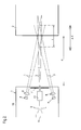
- Figures 1 and 2 is an embodiment of an optoelectronic Device 1 for detecting the height of an object edge shown.
- the object consists of a paper stack 2, which is arranged for example on a printing press or the like.
- the height Z of the paper stack 2 can be in the range ⁇ Z vary.
- the optoelectronic device 1 the height of the forming the object edge Upper edge of the paper stack 2 detected. This is the optoelectronic device 1 is laterally spaced from the paper stack 2 and is located essentially at the height of the top edge of the paper stack 2.
- the distance d of the paper stack 2 to the optoelectronic device 1 can be within of the range ⁇ d vary.
- the optoelectronic device 1 has two emitting light beams 3 Transmitter 4 and a receiver 5 receiving light beams 6 on.
- the transmitters 4 consist of light-emitting diodes.
- the receiver 6 has several adjacent receiving elements 7 and is in the present Embodiment formed by a CCD line element.
- the transmitter 4 and the receiver 6 are in a horizontal plane and are each spaced apart.
- the transmitters 4 are symmetrical arranged on both sides of the receiver 6.
- instead of two Transmitter 4 also several or only one transmitter 4 may be provided.
- the longitudinal axis of the CCD line element is perpendicular to the beam axis of the received light rays 5 reflected back from the paper stack 2 in vertical Direction.
- the Longitudinal axis of the CCD line element in the vertical direction.
- the transmitters 4 each have a cylindrical lens for shaping the transmitted light beams 3 8 upstream, their longitudinal axes each in the vertical direction are arranged progressively.
- the receiver 6 is preferably one of one Upstream of the rotationally symmetrical lens formed receiving optics 9. In front this is a Dove prism 10, which in turn has a receiving aperture 11 is upstream.
- this transmitter 12 is above the level in which the transmitter 4th and the receiver 6 are arranged, another transmitter 12 is arranged, which Pilot transmitted light beams 13 are emitted.
- This transmitter 12 is preferably located together with the receiver 6 in a vertical Level.
- This transmitter 12 is part of a distance sensor. In principle can the transmitter 12 has a further receiver. The distance measurement can take place in particular according to the triangulation principle.
- the receiver 6 is assigned to the transmitter 12, so that no further receiver has to be provided.
- a transmitter optics 14 is arranged downstream of the transmitter 12.
- This transmission optics 14 exists preferably made of a rotationally symmetrical lens and is designed that from the transmitter 12 a parallel beam of pilot light beams 13 is emitted.
- the transmitter 12 can also transmit pilot light beams 13 emit, the beam diameter of which increases with increasing Distance tapers.
- the pilot transmission light beams 13 preferably have a circular beam cross-section. These pilot transmission light beams 13 run obliquely downwards in the direction of the paper stack 2, the front side thereof a part of the pilot transmission light beams 13 as pilot reception light beams 15 reflected back to the optoelectronic device 1.
- All transmitters 4, 12 and the receiver 6 are connected to one, not shown Evaluation unit connected by a microcontroller or the like is formed. All components of the optoelectronic device 1 are arranged in a housing 16, which is not shown Has exit window through which the transmitted light beams 3, the pilot transmitted light beams 13 and the received light beams 5 and the pilot received light beams 15 are performed.
- the upper edge of the paper stack 2 is detected with the transmitted light beams 3.
- the Optoelectronic device 1 is on the side of the upper edge of the paper stack 2 arranged so that the upper edge of the paper stack 2 for the entire Range of variation ⁇ Z of the height of the paper stack 2 and the distances ⁇ d of the Paper stack 2 to the optoelectronic device 1 with the transmitted light beams 3 is illuminated.
- pilot transmission light beams 13 are aligned so that they over the entire height and distance range of the paper stack 2 below the upper edge of the paper stack 2 completely on the substantially flat, meet vertically arranged front of the paper stack 2.
- the spatial distribution of the received light beams with the Dove prism 10 5 or pilot reception light beams 15 in the plane perpendicular to whose beam axes are rotated so that their spatial distributions are complete are mapped onto the CCD line element.
- the transmitter 4 downstream cylindrical lenses 8 such beam shaping of the transmitted light beams 3 achieved that the beam cross sections of the transmitted light beams 3 the shape of elongated ellipses.
- the transmitter 4 are laterally spaced from The upper edge of the paper stack 2 is arranged so that the transmitted light beams 3 the Illuminate the entire height range ⁇ Z, in which the upper edge of the paper stack 2 can lie.
- the beam diameters of the transmitted light beams 3 dimensioned so that this condition for all distances of the Paper stack 2 are met within the range of variation ⁇ d.
- the transmitted light beams 3 overlap Transmitter 4 and the received light rays reflected from the paper stack 2 5 in a predetermined area, the so-called depth of field T.
- the so-called depth of field T Within this range is the upper edge of the paper stack 2 with the transmitted light beams 3 detectable.
- the depth of field T the entire variation range ⁇ d Distance d of the paper stack 2 to the optoelectronic device 1 covers. In this way, the upper edge of the paper stack 2 can be reliably detected guaranteed over the entire range ⁇ d.
- the other part of the transmitted light beams 3 runs above the upper edge of the paper stack 2 past this and does not reach the recipient 6.
- the distribution of the illuminated receiving elements 7 does not yet exist clear measure for the height Z of the paper stack 2. This is due to the fact that in general the distribution of the illuminated receiving elements 7 from the distance d of the paper stack 2 is dependent.
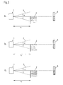
- 3a-c is in each case the optoelectronic device 1 shown in front of the paper stack 2, wherein in the individual FIGS. 3a, b, c the paper stack 2 at different distances d1, d2, d3 (d3> d2> d1) arranged to the optoelectronic device 1 is.
- the height Z of the paper stack 2 is in each case in the optical Axis of the parallel and an opening angle ⁇ Transmitting light beams 3.
- d1, d2, d3 get the same illumination of the receiver 6, which is schematically each behind the arrangement of the device 1 and the paper stack 2 in the figures 3a, b, c is shown.
- the distances d1, d2 and d3 is the Half of the receiving elements 7 illuminated.
- the illuminated part of the Receiver 6 is shown hatched in Figures 3a, b, c.
- FIGS. 4a, b, c essentially correspond the arrangements according to Figures 3a, b, c. Unlike the Arrangements according to Figures 3a, b, c lies with the arrangements according to Figures 4a, b, c, the upper edge of the paper stack 2 by Z1 below the beam axis of the transmitted light beams 3, the opening angle in turn ⁇ is.
- the illuminated part of the Receiver 6 is again shown hatched in FIGS. 4a, b, c.
- the pilot transmitter light beam 13 becomes emitter 12 for calibrating the distributions of illuminated receiving elements 7, which by the received light rays 5 reflected back from the paper stack 2 be used.
- This data is determined during a teach-in process.
- the duration of the learning process is only the pilot light beam 13 emitting Transmitter 12 activated while the other transmitters 4 are deactivated. While the learning process, the distance d of the paper stack 2 to the optoelectronic Device 1 step by step within the entire range of variation ⁇ d changed.
- the light received by the pilot is used 15 received distribution V of the illuminated receiving elements 7 registered and stored in the evaluation unit.
- a characteristic curve of the Distributions V as a function of the distance d from the paper stack 2 to the device 1 received ( Figure 5).
- Geometric beam parameters of the transmitted light beams 3 and the pilot transmitted light beams 13 are used to calibrate the received light beams 5 generated distributions of the illuminated receiving elements 7 used.
- the calibration takes place during the work operation following the teach-in process the optoelectronic device 1. During this operation is initially only the transmitter 12 emitting pilot light beams 13 activated. The current distance value of the paper stack 2 becomes the optoelectronic Device 1 determined. The corresponding one becomes this distance value Characteristic value read out.
- the transmitter 12 emitting pilot light beams 13 is then switched off and the transmit light beams 3 emitting transmitters 4 are used for detection the height Z of the paper stack 2 activated.
- the transmitted light beams 3 and the pilot transmitted light beams are thus in the work mode 13 continuously activated alternately. If the transmitters 4 and 12 transmitted light beams 3 and pilot transmitted light beams 13 with different In principle, the transmitters 4 and 12 can also emit wavelengths simultaneously to be activated.
- the distance sensor has a separate receiver 6
- a characteristic curve as shown in FIG. 5 need not be determined.
- the calibration is carried out directly by means of the distance sensor determined distance value.
Landscapes
- Engineering & Computer Science (AREA)
- Physics & Mathematics (AREA)
- General Physics & Mathematics (AREA)
- Computer Networks & Wireless Communication (AREA)
- Radar, Positioning & Navigation (AREA)
- Remote Sensing (AREA)
- Length Measuring Devices By Optical Means (AREA)
- Measurement Of Optical Distance (AREA)
- Undergarments, Swaddling Clothes, Handkerchiefs Or Underwear Materials (AREA)
- Photo Coupler, Interrupter, Optical-To-Optical Conversion Devices (AREA)
- Control Of Motors That Do Not Use Commutators (AREA)
- Controlling Sheets Or Webs (AREA)
Applications Claiming Priority (2)
| Application Number | Priority Date | Filing Date | Title |
|---|---|---|---|
| DE19914962A DE19914962C2 (de) | 1999-04-01 | 1999-04-01 | Optoelektronische Vorrichtung |
| DE19914962 | 1999-04-01 |
Publications (3)
| Publication Number | Publication Date |
|---|---|
| EP1041394A2 true EP1041394A2 (fr) | 2000-10-04 |
| EP1041394A3 EP1041394A3 (fr) | 2002-02-06 |
| EP1041394B1 EP1041394B1 (fr) | 2004-02-25 |
Family
ID=7903319
Family Applications (2)
| Application Number | Title | Priority Date | Filing Date |
|---|---|---|---|
| EP99117012A Expired - Lifetime EP1041394B1 (fr) | 1999-04-01 | 1999-08-30 | Dispositif opto-électronique |
| EP00106366A Expired - Lifetime EP1041393B1 (fr) | 1999-04-01 | 2000-03-24 | Dispositif optoélectronique |
Family Applications After (1)
| Application Number | Title | Priority Date | Filing Date |
|---|---|---|---|
| EP00106366A Expired - Lifetime EP1041393B1 (fr) | 1999-04-01 | 2000-03-24 | Dispositif optoélectronique |
Country Status (3)
| Country | Link |
|---|---|
| EP (2) | EP1041394B1 (fr) |
| AT (2) | ATE260471T1 (fr) |
| DE (3) | DE19914962C2 (fr) |
Cited By (1)
| Publication number | Priority date | Publication date | Assignee | Title |
|---|---|---|---|---|
| CN117792490A (zh) * | 2021-06-01 | 2024-03-29 | 中国科学院微小卫星创新研究院 | 空间激光通信终端双向传输光学地面智能检测装置及方法 |
Families Citing this family (12)
| Publication number | Priority date | Publication date | Assignee | Title |
|---|---|---|---|---|
| DE10101443B4 (de) * | 2001-01-15 | 2006-04-06 | Leuze Electronic Gmbh & Co Kg | Verfahren zur Ermittlung eines Schnittbildes einer Objektstruktur |
| DE10162279A1 (de) * | 2001-04-22 | 2002-10-31 | Gunther Roeder | Verfahren und Vorrichtung zur Bestimmung der Höhe eines Grates |
| EP1251330A1 (fr) * | 2001-04-22 | 2002-10-23 | Gunther Dipl-.Ing. Röder | Procédé et dispositif pour déterminer la hauteur d'une bavure |
| DE10159540A1 (de) * | 2001-12-05 | 2003-06-26 | Pepperl & Fuchs Visolux Gmbh | Überwachungslichtvorhang |
| DE102004003386C5 (de) * | 2003-02-28 | 2013-07-04 | Leuze Electronic Gmbh & Co. Kg | Optischer Sensor |
| DE102004044341B4 (de) * | 2003-10-13 | 2017-09-07 | Heidelberger Druckmaschinen Ag | Bogendruckmaschine mit optischer Sensoranordnung für einen Bedruckstoff |
| US7489425B2 (en) | 2004-03-15 | 2009-02-10 | Heidelberger Druckmaschinen Ag | Method for controlling an operating process of a printing machine |
| CH697495B1 (de) * | 2005-04-01 | 2008-11-14 | Baumer Electric Ag | Optischer Sensor und Verfahren zur Unterdrückung von Streulichtfehlern. |
| DE102006057878C5 (de) * | 2005-12-24 | 2015-01-22 | Leuze Electronic Gmbh & Co. Kg | Verfahren zur Erfassung von Objekten mittels einer optoelektronischen Vorrichtung |
| DE102010022273A1 (de) † | 2010-05-31 | 2011-12-01 | Sick Ag | Optoelektronischer Sensor zur Detektion von Objektkanten |
| DE102010043723B4 (de) | 2010-11-10 | 2022-03-10 | pmdtechnologies ag | Lichtlaufzeitkamerasystem |
| EP2801786B1 (fr) | 2013-05-08 | 2019-01-02 | Sick AG | Capteur optoélectronique et procédé pour la détection de bords d'objets |
Family Cites Families (5)
| Publication number | Priority date | Publication date | Assignee | Title |
|---|---|---|---|---|
| GB1230912A (fr) * | 1969-04-12 | 1971-05-05 | ||
| DE2104893A1 (de) * | 1971-02-03 | 1972-08-17 | Licentia Gmbh | Vorrichtung zum Abtasten von Kanten bewegter Gegenstände |
| DE2906641A1 (de) * | 1979-02-21 | 1980-08-28 | Freudenberg Carl Fa | Verfahren zur optisch-elektrischen messung des abstandes zwischen einer messeinrichtung und einem pruefling |
| DE3915371C2 (de) * | 1989-05-11 | 1995-05-24 | Roland Man Druckmasch | Einrichtung zur Steuerung der Hubbewegung eines Stapeltischs |
| DE19621120C1 (de) * | 1996-05-24 | 1997-05-07 | Leuze Electronic Gmbh & Co | Optoelektronische Vorrichtung |
-
1999
- 1999-04-01 DE DE19914962A patent/DE19914962C2/de not_active Expired - Fee Related
- 1999-08-30 DE DE59908647T patent/DE59908647D1/de not_active Expired - Fee Related
- 1999-08-30 EP EP99117012A patent/EP1041394B1/fr not_active Expired - Lifetime
- 1999-08-30 AT AT99117012T patent/ATE260471T1/de not_active IP Right Cessation
-
2000
- 2000-03-24 EP EP00106366A patent/EP1041393B1/fr not_active Expired - Lifetime
- 2000-03-24 DE DE50006647T patent/DE50006647D1/de not_active Expired - Fee Related
- 2000-03-24 AT AT00106366T patent/ATE268479T1/de not_active IP Right Cessation
Cited By (1)
| Publication number | Priority date | Publication date | Assignee | Title |
|---|---|---|---|---|
| CN117792490A (zh) * | 2021-06-01 | 2024-03-29 | 中国科学院微小卫星创新研究院 | 空间激光通信终端双向传输光学地面智能检测装置及方法 |
Also Published As
| Publication number | Publication date |
|---|---|
| DE50006647D1 (de) | 2004-07-08 |
| ATE260471T1 (de) | 2004-03-15 |
| EP1041393A3 (fr) | 2002-02-06 |
| ATE268479T1 (de) | 2004-06-15 |
| EP1041393B1 (fr) | 2004-06-02 |
| DE19914962A1 (de) | 2000-10-26 |
| DE19914962C2 (de) | 2003-02-06 |
| DE59908647D1 (de) | 2004-04-01 |
| EP1041393A2 (fr) | 2000-10-04 |
| EP1041394A3 (fr) | 2002-02-06 |
| EP1041394B1 (fr) | 2004-02-25 |
Similar Documents
| Publication | Publication Date | Title |
|---|---|---|
| DE3020483C2 (de) | Fotoelektrische Einrichtung zum Abtasten von Gegenständen | |
| DE102008061035C5 (de) | Verfahren und optischer Sensor zur Erfassung von Objekten | |
| EP1041394B1 (fr) | Dispositif opto-électronique | |
| EP3004789B1 (fr) | Cadre de mesure pour la détermination optique sans contact d'une position de tir et procédé de mesure associé | |
| EP3168642A1 (fr) | Capteur optoélectronique et procédé de détection d'un objet | |
| EP3859379A1 (fr) | Capteur optoélectronique avec filtre de réception adapté à l'angle de vue et procédé de détection des objets | |
| EP1845334A1 (fr) | Capteur optique | |
| DE19852719A1 (de) | Doppelbogen-Erkennungsvorrichtung | |
| EP2447739B2 (fr) | Procédé de détection optique d'objets et bouton lumineux | |
| EP3001226A1 (fr) | Rideau lumineux | |
| EP2801786B1 (fr) | Capteur optoélectronique et procédé pour la détection de bords d'objets | |
| DE102004003386C5 (de) | Optischer Sensor | |
| EP3519857B1 (fr) | Dispositif de détection pour un véhicule automobile, système d'aide à la conduite, véhicule automobile et procédé associé | |
| DE19852412B4 (de) | Lichttaster | |
| EP1134594B1 (fr) | Procédé et dispositif de détection de zones de carré d'objet | |
| DE20216042U1 (de) | Vorrichtung zur Erfassung der Kantenpositionen von Bögen in einer bogenverarbeitenden Maschine | |
| EP1223132B1 (fr) | Dispositif optoélectrique | |
| DE3611535C2 (fr) | ||
| DE202021105507U1 (de) | Optoelektronischer Sensor | |
| EP1148353A2 (fr) | Capteur optique | |
| DE102023122837A1 (de) | Triangulations-Lichttaster | |
| EP4446784A1 (fr) | Capteur optique | |
| DE102013103810B4 (de) | Optischer Sensor | |
| DE102008022545B4 (de) | Optischer Sensor | |
| EP2180347B1 (fr) | Barrière lumineuse de réflexion à rayons multiples et procédé destiné à l'alignement d'une barrière lumineuse de réflexion à rayons multiples |
Legal Events
| Date | Code | Title | Description |
|---|---|---|---|
| PUAI | Public reference made under article 153(3) epc to a published international application that has entered the european phase |
Free format text: ORIGINAL CODE: 0009012 |
|
| 17P | Request for examination filed |
Effective date: 19990921 |
|
| AK | Designated contracting states |
Kind code of ref document: A2 Designated state(s): AT BE CH CY DE DK ES FI FR GB GR IE IT LI LU MC NL PT SE Kind code of ref document: A2 Designated state(s): AT CH DE FR GB LI |
|
| AX | Request for extension of the european patent |
Free format text: AL;LT;LV;MK;RO;SI |
|
| PUAL | Search report despatched |
Free format text: ORIGINAL CODE: 0009013 |
|
| AK | Designated contracting states |
Kind code of ref document: A3 Designated state(s): AT BE CH CY DE DK ES FI FR GB GR IE IT LI LU MC NL PT SE |
|
| AX | Request for extension of the european patent |
Free format text: AL;LT;LV;MK;RO;SI |
|
| RIC1 | Information provided on ipc code assigned before grant |
Free format text: 7G 01S 7/497 A, 7G 01S 7/481 B, 7G 01B 11/06 B |
|
| AKX | Designation fees paid |
Free format text: AT CH DE FR GB LI |
|
| GRAP | Despatch of communication of intention to grant a patent |
Free format text: ORIGINAL CODE: EPIDOSNIGR1 |
|
| GRAS | Grant fee paid |
Free format text: ORIGINAL CODE: EPIDOSNIGR3 |
|
| RAP1 | Party data changed (applicant data changed or rights of an application transferred) |
Owner name: LEUZE ELECTRONIC GMBH + CO KG |
|
| GRAA | (expected) grant |
Free format text: ORIGINAL CODE: 0009210 |
|
| AK | Designated contracting states |
Kind code of ref document: B1 Designated state(s): AT CH DE FR GB LI |
|
| REG | Reference to a national code |
Ref country code: GB Ref legal event code: FG4D Free format text: NOT ENGLISH |
|
| REG | Reference to a national code |
Ref country code: CH Ref legal event code: NV Representative=s name: ROTTMANN, ZIMMERMANN + PARTNER AG Ref country code: CH Ref legal event code: EP |
|
| GBT | Gb: translation of ep patent filed (gb section 77(6)(a)/1977) |
Effective date: 20040225 |
|
| REG | Reference to a national code |
Ref country code: IE Ref legal event code: FG4D Free format text: GERMAN |
|
| REF | Corresponds to: |
Ref document number: 59908647 Country of ref document: DE Date of ref document: 20040401 Kind code of ref document: P |
|
| REG | Reference to a national code |
Ref country code: IE Ref legal event code: FD4D |
|
| ET | Fr: translation filed | ||
| PLBE | No opposition filed within time limit |
Free format text: ORIGINAL CODE: 0009261 |
|
| STAA | Information on the status of an ep patent application or granted ep patent |
Free format text: STATUS: NO OPPOSITION FILED WITHIN TIME LIMIT |
|
| 26N | No opposition filed |
Effective date: 20041126 |
|
| PGFP | Annual fee paid to national office [announced via postgrant information from national office to epo] |
Ref country code: DE Payment date: 20080826 Year of fee payment: 10 Ref country code: CH Payment date: 20080814 Year of fee payment: 10 |
|
| PGFP | Annual fee paid to national office [announced via postgrant information from national office to epo] |
Ref country code: FR Payment date: 20080813 Year of fee payment: 10 Ref country code: AT Payment date: 20080814 Year of fee payment: 10 |
|
| PGFP | Annual fee paid to national office [announced via postgrant information from national office to epo] |
Ref country code: GB Payment date: 20080821 Year of fee payment: 10 |
|
| REG | Reference to a national code |
Ref country code: CH Ref legal event code: PL |
|
| GBPC | Gb: european patent ceased through non-payment of renewal fee |
Effective date: 20090830 |
|
| PG25 | Lapsed in a contracting state [announced via postgrant information from national office to epo] |
Ref country code: LI Free format text: LAPSE BECAUSE OF NON-PAYMENT OF DUE FEES Effective date: 20090831 Ref country code: CH Free format text: LAPSE BECAUSE OF NON-PAYMENT OF DUE FEES Effective date: 20090831 |
|
| REG | Reference to a national code |
Ref country code: FR Ref legal event code: ST Effective date: 20100430 |
|
| PG25 | Lapsed in a contracting state [announced via postgrant information from national office to epo] |
Ref country code: AT Free format text: LAPSE BECAUSE OF NON-PAYMENT OF DUE FEES Effective date: 20090830 |
|
| PG25 | Lapsed in a contracting state [announced via postgrant information from national office to epo] |
Ref country code: FR Free format text: LAPSE BECAUSE OF NON-PAYMENT OF DUE FEES Effective date: 20090831 Ref country code: DE Free format text: LAPSE BECAUSE OF NON-PAYMENT OF DUE FEES Effective date: 20100302 |
|
| PG25 | Lapsed in a contracting state [announced via postgrant information from national office to epo] |
Ref country code: GB Free format text: LAPSE BECAUSE OF NON-PAYMENT OF DUE FEES Effective date: 20090830 |