EP1041665A1 - Lignes de transmission à rubans pour antennes de satellites - Google Patents
Lignes de transmission à rubans pour antennes de satellites Download PDFInfo
- Publication number
- EP1041665A1 EP1041665A1 EP00302690A EP00302690A EP1041665A1 EP 1041665 A1 EP1041665 A1 EP 1041665A1 EP 00302690 A EP00302690 A EP 00302690A EP 00302690 A EP00302690 A EP 00302690A EP 1041665 A1 EP1041665 A1 EP 1041665A1
- Authority
- EP
- European Patent Office
- Prior art keywords
- strip
- conductor strip
- bonded
- transmission line
- thin
- Prior art date
- Legal status (The legal status is an assumption and is not a legal conclusion. Google has not performed a legal analysis and makes no representation as to the accuracy of the status listed.)
- Withdrawn
Links
Images




Classifications
-
- H—ELECTRICITY
- H01—ELECTRIC ELEMENTS
- H01P—WAVEGUIDES; RESONATORS, LINES, OR OTHER DEVICES OF THE WAVEGUIDE TYPE
- H01P3/00—Waveguides; Transmission lines of the waveguide type
- H01P3/02—Waveguides; Transmission lines of the waveguide type with two longitudinal conductors
- H01P3/08—Microstrips; Strip lines
- H01P3/085—Triplate lines
-
- H—ELECTRICITY
- H01—ELECTRIC ELEMENTS
- H01P—WAVEGUIDES; RESONATORS, LINES, OR OTHER DEVICES OF THE WAVEGUIDE TYPE
- H01P11/00—Apparatus or processes specially adapted for manufacturing waveguides or resonators, lines, or other devices of the waveguide type
- H01P11/001—Manufacturing waveguides or transmission lines of the waveguide type
- H01P11/003—Manufacturing lines with conductors on a substrate, e.g. strip lines, slot lines
-
- H—ELECTRICITY
- H01—ELECTRIC ELEMENTS
- H01P—WAVEGUIDES; RESONATORS, LINES, OR OTHER DEVICES OF THE WAVEGUIDE TYPE
- H01P3/00—Waveguides; Transmission lines of the waveguide type
- H01P3/02—Waveguides; Transmission lines of the waveguide type with two longitudinal conductors
- H01P3/08—Microstrips; Strip lines
- H01P3/088—Stacked transmission lines
-
- H—ELECTRICITY
- H01—ELECTRIC ELEMENTS
- H01P—WAVEGUIDES; RESONATORS, LINES, OR OTHER DEVICES OF THE WAVEGUIDE TYPE
- H01P5/00—Coupling devices of the waveguide type
- H01P5/08—Coupling devices of the waveguide type for linking dissimilar lines or devices
- H01P5/085—Coaxial-line/strip-line transitions
Definitions
- Space-borne antennas were individually designed and assembled for a particular satellite, usually launched for a specific purpose. Each element of the many elements of the antenna had to be individually fabricated and assembled. Thus, the antenna was very expensive to fabricate and assemble.
- US Patent 5,539,415 discloses an inexpensive, small, compact, light weight, easy to assemble, multibeam or phased array device useful as a direct radiating array or as a feed for a reflector or lens antenna.
- the device employs an array of planar radiators coupled to radio frequency (R.F.) transmission lines to form individual feed or antenna strips.
- the feed or antenna strips are coupled into a filter to pass the desired band of frequencies and reject undesirable bands of frequencies.
- the filters are coupled to Monolithic Microwave Integrated Circuit (MMIC) amplifiers that contain N amplifiers with an integral isolator.
- Amplifiers are Solid State Power Amplifiers (SSPA's) or Low Noise Amplifiers (LNA's). SSPA's are used for the transmit mode and LNA's are used for the receive mode. Amplifiers are utilized to amplify the aforementioned RF signals.
- SSPA's Solid State Power Amplifiers
- LNA's Low Noise Amplifiers
- a microwave transmission line configuration known as bonded strip transmission line is formed from two solid dielectric substrates with metal foil (usually copper) bonded or plated to one or both flat sides of each substrate.
- the substrates are bonded together under pressure and at elevated temperature to form a sealed package.
- the foil is configured (usually by photo etching) to have two metal ground planes with one or more metal strip conductors in the middle to form a strip transmission line.
- the middle conductor can be formed (usually by photo etching) to produce various microwave circuits. Channelization may be used to prevent unwanted parallel plate modes.
- bar line and suspended air strip transmission lines are composed of one or more metal bars or thin dielectric supported strips located midway between two metal ground planes forming a microwave transmission line.
- the middle bar in bar lines is suspended between the ground planes using low dielectric constant honeycomb or foam.
- the package for bar line and for suspended air strip transmission lines is held together by mechanically clamping, usually with bolts or screw fasteners.
- the previously-known structures for microwave transmission lines of the aforementioned types have important disadvantages with respect to their electrical and/or their physical properties such as strength and weight.
- the barline and suspended air strip transmission lines arc composed of unbonded layers, mechanically fastened together, requiring thicker structural panels and numerous mechanical fasteners to provide a good degree of mechanical performance under sheer and tension forces.
- the resulting barline and suspended air strip transmission line configurations are heavy and have a high weight to strength ratio. Also, they are composed of individual components: machined ground planes, conducting bars for the barline and photo etched strips for the suspended air strip transmission line, and foam or honeycomb cores mechanically held together with fasteners requiring substantial assembly time and labor intensive methods used to fabricate and assemble the barline and suspended air strip transmission line packages.
- the present invention provides a method for producing improved RF transmission lines for satellite antennas and beamforming networks, comprising the steps of (1) bonding together (a) a central conductor strip or trace strip comprising a dielectric layer or circuit board having on one or both surfaces thereof conductive strip circuitry; (b) upper and lower core layers of lightweight closed-cell plastic foam bonded to (a), and (c) upper and lower surface layers or faceskins of conductive metal foil or of dielectric material bonded to metal foil layers inside and/or outside, or solid metal plates, to form ground planes, bonded to the surfaces of the adjacent foam core layers, (2) boring holes or vias through the ground plane or through the central conductor strips, core layers and ground plane, layers and the core layers, and (3) plating the bores or vias with an electroconductive metal, usually copper, to provide a plurality of electroconductive connections between the ground planes, for parallel plate propagating mode suppression, or between central conductor strips to connect independent assemblies.
- an electroconductive metal usually copper
- the invention also provides a bonded air strip microwave transmission line assembly for satellite antennas and beamforming networks, comprising: a thin central conductor strip or trace; an opposed pair of upper and lower solid dielectric core layer(s) of lightweight plastic foam adhesively bonded to confine the conductor strip therebetween; an opposed outer pair of thin conductive faceskins, each adhesively bonded to the outer surface of one of said dielectric foam layers; at least one hole or via through said conductive faceskins and through said dielectric core layers, and a continuous conductive material which coats or fills said hole or vias to provide conductive contact between said conductive faceskins to suppress parallel plate propagating modes during use.
- the strip transmission line (STL) component 10 thereof is a bonded composite assembly of a center conductor strip 11 comprising a dielectric support 12 having bonded to one or both sides thereof (as shown) narrow elongate metal layers or foils 13.
- the center strip 11 is bonded between lightweight plastic foam core layers 14 and 15 by means of a resinous adhesive at elevated temperature and pressure, and thin faceskins 16 and 17 are similarly adhesive-bonded to the upper and lower surfaces of the core layers 14 and 15, respectively.
- the illustrated faceskins 16 and 17 each comprise a dielectric or metal support 18 or 19 and an inner conductive metal foil 20 or 21 bonded thereto, adjacent the foam core layer 14 or 15.
- the conductive metal foils 20 and 21 form ground planes on the composite assembly.
- the ground planes are electrically united by conductive connections.
- Such connections are produced in the present STL assemblies by forming bores 22 or vias through the faceskins 16, 17 and foam core layers 14, 15 and the dielectric support 12 of the center strip 11, and coating or plating the inner walls of the bores 22 with a continuous layer 23 of conductive material such as electroless copper as used in the printed circuit board art.
- the conductive layer 23 in each bore 22 connects electrically with the conductive metal foil layers 20 and 21 on the opposed faceskins 16 and 17 to produce electrical conductivity between the faceskins for mode suppression.
- the faceskins 16 and 17 may have the foil layers 20 and 21 on either the inner or outer surface of the dielectric layer 18 or 19, or on both surfaces. Also it is possible to use conductive metal foil or metal plate, per se, without the need for the dielectric support layer 18 or 19.
- the bonded composite assembly of Fig 1 is integral, strong and lightweight and derives its strength from the fact that the various layers thereof are bonded to one another and cannot slip or slide under sheer and tension forces relative to one another. Also, it is fabricated using high speed, mass production printed circuit board (PCB) techniques including photo-etching, bonding, routing, drilling and plating or via-filling, resulting in a unitary fabricated unit requiring minimum assembly.
- PCB printed circuit board
- the present invention is advantageous for the following reasons:
- this invention is advantageous for the following reason: a. Due to the lower dielectric constant, the width of the strip conductor will be wider for high impedance characteristic and, therefore, less sensitive to etching tolerances.
- this invention is advantageous for the following reason: a.
- the foam core is much lighter than solid dielectric material resulting in a lighter configuration.
- the present assemblies are sandwich constructions of face plates and core material, and the strength and stiffness are determined primarily by the thickness of the core material (ground plane spacing). Therefore, the invention is advantageous for the following reasons:
- the connector 35 is a commercially-available STL component comprising a metal housing 45 having a U-shaped attachment section 46 and a receptacle section 47 surrounding a terminal 48 which is electrically connected with the center trace 39 by being mechanically pressed or soldered thereto at area 49.
- the connector housing section 46 is mechanically fastened to the unitary STL component by means of bolts or fasteners 50 through bores drilled through the foam or solid dielectric material 37a at the connector end of the STL assembly 36.
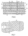
- Figs 6 and 7 illustrate integrations or interconnections between otherwise independent different STL members to form a unitary strong assembly, without the need for conventional connectors.
- a two step bonding process is used to interconnect two separate assemblies without the need for external connectors.
- Subassembly 6a is formed by bonding together the center dielectric layers or circuit boards having metal foil 51 and 52, their respective foam core layers 54 and the central ground planes 56. Two metal ground planes are shown, however, a single plane may be used.
- the desired circuitry is then formed on metal foil 51 and 52, usually by photo-etching.
- the subassembly 6a is then drilled and plated through hole or via 57 is formed by plating metal, usually electroless copper, to the edges of the via 58, electrically connecting the circuits on 51 and 52 to form a RF via.
- any printed circuit patch-type antenna(s) can be formed, usually by photoetching, into one or more of the outermost circuit layers with the outermost ground planes omitted.
- the patch-type antenna(s) can be fed directly from circuitry on the same layer or can be connected to internal circuitry with electromagnetically-coupled probe(s), slot(s) or plated-through vias(s).
- Circuit layer 74 of Fig 12 can have a long trace length between either or both plated through interconnects 77 and the quarter wavelength overlapping lines.
- Multistep drilling and plating will accommodate any required channelization for unwanted parallel plate modes in any or all of the layers including any necessary joining together electrically of configurations using metal foil on the top and bottom of thin substrate material.
- the entire assembly may be edge plated with metal to suppress electromagnetic interferences and intermodulation products while providing a hermetically sealed package.
- Side launch connectors can be mounted to the outside ground planes, or with the proper edge extensions of ground planes and center conductor traces, end launch connectors may be used to electrically connect to the assembly.
- Any printed circuit slot type antenna element(s) can be etched into one or both outside ground planes and connected to internal circuitry with electromagnetic coupled probe(s) or with a plated through hole(s).
- any printed circuit patch type antenna element(s) can be etched into one or more of the outermost circuit layer(s) with the outermost ground planes omitted. The patches can be fed directly from circuitry on the same layer or connected to internal circuitry with electromagnetic coupling probe(s), slot(s), or plated through holes.
Landscapes
- Engineering & Computer Science (AREA)
- Manufacturing & Machinery (AREA)
- Waveguide Aerials (AREA)
- Waveguides (AREA)
- Details Of Aerials (AREA)
- Variable-Direction Aerials And Aerial Arrays (AREA)
Applications Claiming Priority (2)
| Application Number | Priority Date | Filing Date | Title |
|---|---|---|---|
| US283501 | 1999-04-01 | ||
| US09/283,501 US6356245B2 (en) | 1999-04-01 | 1999-04-01 | Microwave strip transmission lines, beamforming networks and antennas and methods for preparing the same |
Publications (1)
| Publication Number | Publication Date |
|---|---|
| EP1041665A1 true EP1041665A1 (fr) | 2000-10-04 |
Family
ID=23086359
Family Applications (1)
| Application Number | Title | Priority Date | Filing Date |
|---|---|---|---|
| EP00302690A Withdrawn EP1041665A1 (fr) | 1999-04-01 | 2000-03-30 | Lignes de transmission à rubans pour antennes de satellites |
Country Status (3)
| Country | Link |
|---|---|
| US (1) | US6356245B2 (fr) |
| EP (1) | EP1041665A1 (fr) |
| JP (1) | JP2000349513A (fr) |
Cited By (5)
| Publication number | Priority date | Publication date | Assignee | Title |
|---|---|---|---|---|
| WO2005025001A1 (fr) * | 2003-09-03 | 2005-03-17 | Raytheon Company | Interconnexion verticale rf integree pour antenne conformee souple |
| WO2008040337A1 (fr) * | 2006-10-06 | 2008-04-10 | Epcos Ag | Substrat comprenant une ligne adaptée aux hautes fréquences |
| EP2365577A1 (fr) * | 2010-03-09 | 2011-09-14 | Raytheon Company | Structures de ligne de transmission à couche de mousse |
| FR2970815A1 (fr) * | 2011-01-26 | 2012-07-27 | Bouygues Telecom Sa | Jonction triplaque-coaxial d'une antenne a technologie imprimee et antenne correspondante |
| EP2887452A1 (fr) * | 2013-12-18 | 2015-06-24 | Arvind Swarup | Ensembles de circuit de ligne de transmission et procédés de fabrication |
Families Citing this family (24)
| Publication number | Priority date | Publication date | Assignee | Title |
|---|---|---|---|---|
| SE514408C2 (sv) * | 1999-06-17 | 2001-02-19 | Ericsson Telefon Ab L M | Elektrisk transmissionsanordning |
| CN1316858C (zh) * | 2001-04-27 | 2007-05-16 | 日本电气株式会社 | 高频电路基板及其制造方法 |
| US6703114B1 (en) * | 2002-10-17 | 2004-03-09 | Arlon | Laminate structures, methods for production thereof and uses therefor |
| US6947008B2 (en) * | 2003-01-31 | 2005-09-20 | Ems Technologies, Inc. | Conformable layered antenna array |
| US7271767B2 (en) * | 2003-11-26 | 2007-09-18 | The Boeing Company | Beamforming architecture for multi-beam phased array antennas |
| SE526987C2 (sv) * | 2004-04-15 | 2005-11-29 | Cellmax Technologies Ab | Matningsnät för antenner |
| TWM260885U (en) * | 2004-07-09 | 2005-04-01 | Inpaq Technology Co Ltd | Antenna structure |
| US8414962B2 (en) | 2005-10-28 | 2013-04-09 | The Penn State Research Foundation | Microcontact printed thin film capacitors |
| KR20090006336A (ko) | 2007-07-11 | 2009-01-15 | 삼성전기주식회사 | 케이스 일체형 안테나 및 그 제조방법 |
| US8152800B2 (en) * | 2007-07-30 | 2012-04-10 | Vivant Medical, Inc. | Electrosurgical systems and printed circuit boards for use therewith |
| SE531633C2 (sv) * | 2007-09-24 | 2009-06-16 | Cellmax Technologies Ab | Antennarrangemang |
| SE531826C2 (sv) | 2007-09-24 | 2009-08-18 | Cellmax Technologies Ab | Antennarrangemang |
| KR100914440B1 (ko) | 2007-09-28 | 2009-08-28 | 삼성전기주식회사 | 단차가 형성된 전도층을 갖는 인쇄회로기판 |
| FR2942569B1 (fr) * | 2009-02-25 | 2011-03-25 | Alcatel Lucent | Dispositif de connexion pour un cable coaxial transportant un signal haute frequence. |
| DE102012111382A1 (de) * | 2012-11-23 | 2014-05-28 | GAT Gesellschaft für Antriebstechnik mbH | Antennenstruktur zur breitbandigen Übertragung elektrischer Signale |
| JP6054211B2 (ja) * | 2013-03-07 | 2016-12-27 | 株式会社東芝 | アレーアンテナ装置 |
| CN103647127B (zh) * | 2013-12-09 | 2017-02-01 | 上海贝尔股份有限公司 | 用于将同轴电缆耦接至带状线的连接器 |
| KR101784501B1 (ko) * | 2016-02-03 | 2017-11-07 | 블루웨이브텔(주) | 고효율 알에프 전송선로 구조 및 상기 구조를 이용한 이중 직교 편파를 갖는 송수신 배열 안테나 장치 |
| ES2902721T3 (es) | 2017-09-26 | 2022-03-29 | Merit Automotive Electronics Systems S L U | Teclado elastomérico |
| US11122689B2 (en) | 2017-10-18 | 2021-09-14 | Mbda Uk Limited | Circuit assembly |
| GB201717121D0 (en) * | 2017-10-18 | 2017-11-29 | Mbda Uk Ltd | Circuit Assembly |
| US20190150296A1 (en) * | 2017-11-10 | 2019-05-16 | Raytheon Company | Additive manufacturing technology microwave vertical launch |
| US20220158336A1 (en) * | 2019-03-29 | 2022-05-19 | Autonetworks Technologies, Ltd. | Wiring module |
| EP4211996A1 (fr) * | 2020-09-10 | 2023-07-19 | Sew-Eurodrive GmbH & Co. KG | Procédé et système de production de pièce coulée pour la production d'un carter de moteur électrique, et moteur électrique |
Citations (6)
| Publication number | Priority date | Publication date | Assignee | Title |
|---|---|---|---|---|
| US3768048A (en) * | 1971-12-21 | 1973-10-23 | Us Army | Super lightweight microwave circuits |
| US3825861A (en) * | 1973-09-10 | 1974-07-23 | Eg & G Inc | Coaxial line to strip line connector |
| US3880723A (en) * | 1973-08-28 | 1975-04-29 | Us Air Force | Method of making substrates for microwave microstrip circuits |
| US4605915A (en) * | 1984-07-09 | 1986-08-12 | Cubic Corporation | Stripline circuits isolated by adjacent decoupling strip portions |
| US5227742A (en) * | 1982-07-02 | 1993-07-13 | Junkosha Co., Ltd. | Stripline cable having a porous dielectric tape with openings disposed therethrough |
| EP0800225A2 (fr) * | 1996-04-03 | 1997-10-08 | Nortel Networks Corporation | Arrangement pour terminaison de câble coaxial |
Family Cites Families (5)
| Publication number | Priority date | Publication date | Assignee | Title |
|---|---|---|---|---|
| US3587110A (en) * | 1969-07-01 | 1971-06-22 | Rca Corp | Corporate-network printed antenna system |
| US5768109A (en) * | 1991-06-26 | 1998-06-16 | Hughes Electronics | Multi-layer circuit board and semiconductor flip chip connection |
| US5483380A (en) * | 1992-10-26 | 1996-01-09 | Olympus Optical Co., Ltd. | Compact zoom lens system having high zoom ratio and wide view angle |
| US5539415A (en) * | 1994-09-15 | 1996-07-23 | Space Systems/Loral, Inc. | Antenna feed and beamforming network |
| US5906042A (en) * | 1995-10-04 | 1999-05-25 | Prolinx Labs Corporation | Method and structure to interconnect traces of two conductive layers in a printed circuit board |
-
1999
- 1999-04-01 US US09/283,501 patent/US6356245B2/en not_active Expired - Fee Related
-
2000
- 2000-03-30 EP EP00302690A patent/EP1041665A1/fr not_active Withdrawn
- 2000-03-31 JP JP2000096175A patent/JP2000349513A/ja active Pending
Patent Citations (6)
| Publication number | Priority date | Publication date | Assignee | Title |
|---|---|---|---|---|
| US3768048A (en) * | 1971-12-21 | 1973-10-23 | Us Army | Super lightweight microwave circuits |
| US3880723A (en) * | 1973-08-28 | 1975-04-29 | Us Air Force | Method of making substrates for microwave microstrip circuits |
| US3825861A (en) * | 1973-09-10 | 1974-07-23 | Eg & G Inc | Coaxial line to strip line connector |
| US5227742A (en) * | 1982-07-02 | 1993-07-13 | Junkosha Co., Ltd. | Stripline cable having a porous dielectric tape with openings disposed therethrough |
| US4605915A (en) * | 1984-07-09 | 1986-08-12 | Cubic Corporation | Stripline circuits isolated by adjacent decoupling strip portions |
| EP0800225A2 (fr) * | 1996-04-03 | 1997-10-08 | Nortel Networks Corporation | Arrangement pour terminaison de câble coaxial |
Cited By (11)
| Publication number | Priority date | Publication date | Assignee | Title |
|---|---|---|---|---|
| WO2005025001A1 (fr) * | 2003-09-03 | 2005-03-17 | Raytheon Company | Interconnexion verticale rf integree pour antenne conformee souple |
| US6992629B2 (en) | 2003-09-03 | 2006-01-31 | Raytheon Company | Embedded RF vertical interconnect for flexible conformal antenna |
| WO2008040337A1 (fr) * | 2006-10-06 | 2008-04-10 | Epcos Ag | Substrat comprenant une ligne adaptée aux hautes fréquences |
| US7940144B2 (en) | 2006-10-06 | 2011-05-10 | Epcos Ag | Substrate with embedded signal line and ground planes with a slot therein |
| DE102006047427B4 (de) * | 2006-10-06 | 2012-10-25 | Epcos Ag | Substrat mit HF-tauglicher Leitung |
| EP2365577A1 (fr) * | 2010-03-09 | 2011-09-14 | Raytheon Company | Structures de ligne de transmission à couche de mousse |
| US8482477B2 (en) | 2010-03-09 | 2013-07-09 | Raytheon Company | Foam layer transmission line structures |
| FR2970815A1 (fr) * | 2011-01-26 | 2012-07-27 | Bouygues Telecom Sa | Jonction triplaque-coaxial d'une antenne a technologie imprimee et antenne correspondante |
| WO2012101224A1 (fr) * | 2011-01-26 | 2012-08-02 | Bouygues Telecom | Jonction triplaque-coaxial d'une antenne a technologie imprimee et antenne correspondante |
| EP2887452A1 (fr) * | 2013-12-18 | 2015-06-24 | Arvind Swarup | Ensembles de circuit de ligne de transmission et procédés de fabrication |
| US9634371B2 (en) | 2013-12-18 | 2017-04-25 | Com Dev International Ltd. | Transmission line circuit assemblies and processes for fabrication |
Also Published As
| Publication number | Publication date |
|---|---|
| JP2000349513A (ja) | 2000-12-15 |
| US6356245B2 (en) | 2002-03-12 |
| US20020000932A1 (en) | 2002-01-03 |
Similar Documents
| Publication | Publication Date | Title |
|---|---|---|
| US6356245B2 (en) | Microwave strip transmission lines, beamforming networks and antennas and methods for preparing the same | |
| CN109004375B (zh) | 天线集成印刷线路板及其制造方法 | |
| US7884773B1 (en) | Horn antenna array | |
| US7236070B2 (en) | Electronic component module and manufacturing method thereof | |
| EP0600638B1 (fr) | Méthode et appareil pour l'interconnexion des circuits radiofréquences(RF) intégrés monolithiques à micro-ondes | |
| US8059049B2 (en) | Dual band active array antenna | |
| EP2449621B1 (fr) | Antenne hybride inclinée à ouverture unique | |
| US6765455B1 (en) | Multi-layered spiral couplers on a fluropolymer composite substrate | |
| US8362856B2 (en) | RF transition with 3-dimensional molded RF structure | |
| US20190150296A1 (en) | Additive manufacturing technology microwave vertical launch | |
| JP2006191077A (ja) | 導波管‐プリント基板(pwb)相互接続 | |
| EP2408066B1 (fr) | Systèmes et procédés pour exciter des radiateurs à longue rainure d'une antenne RF | |
| EP3563447B1 (fr) | Système d'interconnexion pour circuit radiofréquence multicouche et procédé de fabrication | |
| US5404145A (en) | Patch coupled aperature array antenna | |
| EP3984097B1 (fr) | Formeur de faisceaux modulaire à interverrouillage | |
| GB2237451A (en) | Multilayer through hole connections | |
| WO2018022308A2 (fr) | Élément de rayonnement en mousse | |
| US3971125A (en) | Method of making an antenna array using printed circuit techniques | |
| US5278574A (en) | Mounting structure for multi-element phased array antenna | |
| US7109830B2 (en) | Low cost highly isolated RF coupler | |
| US6690252B2 (en) | RF circuit assembly | |
| WO2006070206A1 (fr) | Cartes a circuit imprime | |
| KR20050005433A (ko) | 나선형 결합기 | |
| KR20070007399A (ko) | 리드가 부착된 융착 본딩 조립체 | |
| US5384555A (en) | Combined RF and digital/DC signalling interconnect laminate |
Legal Events
| Date | Code | Title | Description |
|---|---|---|---|
| PUAI | Public reference made under article 153(3) epc to a published international application that has entered the european phase |
Free format text: ORIGINAL CODE: 0009012 |
|
| AK | Designated contracting states |
Kind code of ref document: A1 Designated state(s): DE FR GB IT |
|
| AX | Request for extension of the european patent |
Free format text: AL;LT;LV;MK;RO;SI |
|
| 17P | Request for examination filed |
Effective date: 20001122 |
|
| AKX | Designation fees paid |
Free format text: DE FR GB IT |
|
| STAA | Information on the status of an ep patent application or granted ep patent |
Free format text: STATUS: THE APPLICATION HAS BEEN WITHDRAWN |
|
| 18W | Application withdrawn |
Effective date: 20030709 |