EP1041748A2 - Stabilisateur de fréquence pour une source lumineuse pour la communication optique - Google Patents
Stabilisateur de fréquence pour une source lumineuse pour la communication optique Download PDFInfo
- Publication number
- EP1041748A2 EP1041748A2 EP00106113A EP00106113A EP1041748A2 EP 1041748 A2 EP1041748 A2 EP 1041748A2 EP 00106113 A EP00106113 A EP 00106113A EP 00106113 A EP00106113 A EP 00106113A EP 1041748 A2 EP1041748 A2 EP 1041748A2
- Authority
- EP
- European Patent Office
- Prior art keywords
- light
- signal
- light source
- modulated
- phase difference
- Prior art date
- Legal status (The legal status is an assumption and is not a legal conclusion. Google has not performed a legal analysis and makes no representation as to the accuracy of the status listed.)
- Withdrawn
Links
Images



Classifications
-
- H—ELECTRICITY
- H04—ELECTRIC COMMUNICATION TECHNIQUE
- H04B—TRANSMISSION
- H04B10/00—Transmission systems employing electromagnetic waves other than radio-waves, e.g. infrared, visible or ultraviolet light, or employing corpuscular radiation, e.g. quantum communication
- H04B10/50—Transmitters
- H04B10/58—Compensation for non-linear transmitter output
-
- H—ELECTRICITY
- H04—ELECTRIC COMMUNICATION TECHNIQUE
- H04B—TRANSMISSION
- H04B10/00—Transmission systems employing electromagnetic waves other than radio-waves, e.g. infrared, visible or ultraviolet light, or employing corpuscular radiation, e.g. quantum communication
- H04B10/50—Transmitters
- H04B10/501—Structural aspects
- H04B10/506—Multiwavelength transmitters
-
- H—ELECTRICITY
- H04—ELECTRIC COMMUNICATION TECHNIQUE
- H04B—TRANSMISSION
- H04B10/00—Transmission systems employing electromagnetic waves other than radio-waves, e.g. infrared, visible or ultraviolet light, or employing corpuscular radiation, e.g. quantum communication
- H04B10/50—Transmitters
- H04B10/572—Wavelength control
Definitions
- the present invention relates to frequency stabilizing equipment suitably applicable to a light source used in wavelength division multiplexing (hereinafter referred to as "WDM") optical communication and more particularly to the frequency stabilizing equipment for improving accuracy and stability of a frequency of light from the light source employed in optical communication.
- WDM wavelength division multiplexing
- frequency stabilizing equipment for a light source which is comprised of a light source having a control circuit adapted to adjust a frequency of carrier light for optical communication, a light modulator to modulate intensity of carrier light outputted from the light source by using a marker signal, a delay generator to provide time delay to the carrier light to be modulated based on wavelengths of the carrier light modulated by the modulator, a photoelectric converter to convert the time delay given by the delay generator to an electric signal, a phase difference detector to detect the time delay in accordance with the electric signal fed by the photoelectric converter and a control signal generator to generate a control signal to be used in the control circuit in the light source based on a detection signal fed from the phase difference detector.
- the control circuit in the light source employed in the frequency stabilizing equipment is adapted to control so that the carrier light from the light source has a predetermined frequency based on a phase difference between the marker signal used as a modulation signal and carrier light to be modulated to which the time delay has been provided by the delay generator and the provided time delay has been converted to the electric signal.
- frequency stabilizing equipment for optical communication light source comprising:
- a preferable mode is one wherein the local oscillating light source is given a feedback control to maintain a predetermined light intensity.
- a preferable mode is one wherein the optical coupling device is a coupler.
- a preferable mode is one wherein the delay generator is a dispersion generator.
- a preferable mode is one wherein the marker signal is a modulated signal having a predetermined angular velocity.
- frequency stabilizing equipment for optical communication light source comprising;
- the frequency stabilizing equipment further comprises a photoelectric converter to convert the modulated carrier light provided by the delay generator into an electrical signal and to output the electrical signal to the phase difference detector, whereby the photoelectric converter is comprised of a local oscillating light source to produce a local oscillating signal having a wavelength being different from that of the carrier light, an optical coupling device to bind the local oscillating light signal fed from the local oscillating light source to the modulated carrier light from the delay generator in order to optically amplify the modulated carrier light from the delay generator and a light receiver having a non-linearity characteristic between an input signal and output signal to receive a light signal from the coupling device and to output an electrical signal amplified non-linearly to the phase difference detector.
- the photoelectric converter is comprised of a local oscillating light source to produce a local oscillating signal having a wavelength being different from that of the carrier light
- an optical coupling device to bind the local oscillating light signal fed from the local oscillating light source to the modulated carrier
- the local oscillating light source is given a feedback control to maintain a predetermined light intensity.
- the optical coupling device is a coupler.
- the delay generator is a dispersion generator.
- the marker signal is a modulated signal having a predetermined angular velocity.
- amplitude modulation is performed on carrier light used for optical communication by using a marker signal used as a modulation signal having a specified angular velocity which is set arbitrarily with the use of the light modulator.
- the amplitude-modulated light signal is then fed to a delay generator having wavelength-dependency on delay time.
- the light signal outputted by the delay generator is converted to an electric signal by a photoelectric converter.
- the wavelength can be determined by detecting a difference in phase between the light signal inputted into this delay generator and the light signal outputted from the delay generator.
- the phase difference can be detected by converting the amplitude-modulated light outputted from the delay generator to an electric signal using the photoelectric converter and retrieving an envelope signal and by comparing the envelope signal with the modulated light signal.
- the photoelectric converter is provided with a local oscillating light source to output a local oscillating light signal having a wavelength being different from that of the modulated light and adapted to mix the local oscillating light signal with a light signal to be converted photoelectrically.
- a light receiver adapted to have a nonlinear characteristic between inputted light signal and outputted electric signal, the mixed outputted light is converted photoelectrically.
- a multiplication signal between the light signal and the local oscillating light signal is produced and, by using suitably_amplified division signal, the phase difference can be successfully detected.
- FIG. 1 is a schematic block diagram showing stabilizing equipment 10 for a light source device 11 used in WDM (Wavelength Division Multiplexing) optical communication.
- the light source device 11 for the WDM optical communication provided with stabilizing equipment 10 is comprised of n-pieces of light source boards CH1 to CHn, a light switch 1, an external modulator 2, a dispersion generator 3, a photoelectric converter 4, a phase difference detector P1 and a comparator R1.
- Each of the n-pieces of the light source boards CH1 to CHn is a light signal generating section to form one communication channel.
- Each of the light source boards forming the communication channels is provided with a light source (any one of LD1 to LDn), a temperature controlling circuit (any one of TEC1 to TECn) and a coupler (any one of A1 to An).
- Each of the light sources (any one of LD1 to LDn) is composed of a laser diode adapted to oscillate light at wavelengths of ⁇ ( ⁇ 1 to ⁇ n ).Each of the light sources is operative to output carrier light, i.e., modulated light to be used for optical communication having its own wavelength.
- the temperature controlling circuit (TEC1 to TECn) is a section used to change oscillation frequency of the light source (LD1 to LDn) by a control signal (which is described later in detail).
- the coupler (A1 to An) is a section used to separate a part of the modulated light Ec for every channel and to take it out.
- the light switch 1 is a switch used to select one channel out of n-pieces of channels formed by the n-pieces of light source boards (CH1 to CHn).
- the external modulator 2 is a section used to receive a part of modulated light Ec transmitted through the channel formed by the n-pieces of the light source boards (CH1 to CHn) and to perform amplitude-modulation on the modulated light Ec by using a marker signal Em having a predetermined angular velocity which is arbitrarily set in advance. It is composed of, for example, single crystal of lithium niobate or the like.
- the dispersion generator 3 receives the amplitude-modulated light signal Eo from the external modulator 2 and performs dispersion of its wavelength by using, for example, a chirped fiber black grating (hereafter referred to as a "CFBG").
- CFBG chirped fiber black grating
- the photoelectric converter 4 receives the wavelength-dispersed light signal Ed and mixes it with the local oscillating light signal Ee having a wavelength being different from that of the above modulated light Ec.
- a photoelectric conversion is performed on the mixed light signals Ed + Ee by using a light receiver 8 which shows a non-linearity characteristic between an input light signal and an output electric signal.
- a multiplication signal Es is produced which is obtained by multiplying the local oscillating light signal Ee by the wavelength-dispersed light signal Ed.
- the photoelectric converter 4 is comprised of a coupler B, a local oscillating light source 5, a temperature adjusting circuit 6, an output power adjusting circuit 7 and a light receiver 8.
- the coupler B is operative to mix the wavelength-dispersed light signal fed from the above dispersion generator 3 with the local oscillating light signal Ee described later in detail.
- the local oscillating light source 5 is a light source used to output the local oscillating light signal Ee having a wavelength being different from that of the said modulated light Ec.
- This light source a laser diode being capable of monitoring backlight using a photodiode is ordinarily used.
- the temperature adjusting circuit 6 and the output power adjusting circuit 7 are circuits used for compensating changes caused by an output from the local oscillating light source 5.
- the light receiver 8 is a photodiode which shows a non-linearity characteristic between an input light signal and an output electric signal.
- the light receiver 8 is operative to receive the signal Ed + Ee obtained by mixing the wavelength-dispersed light signal Ed with the local oscillating light signal Ee and to perform photoelectric conversion on it and to produce the multiplication signal Es obtained by multiplying the local oscillating signal Ee by the dispersed light signal Ed.
- the principle on which the multiplication signal Es is produced will be described later in detail.
- the amplifier 9 is operative to amplify the electric signal converted by the photoelectric converter 4.
- the phase difference detector P is a section used to obtain a control signal to stabilize an oscillation frequency of the light from the light sources (LD1 to LDn) for every channel. It is further provided with a band-pass filter BPF1, a mixer MIX1 and a low-pass filter LPF1.
- the band-pass filter BPF1 is a filter used to extract only the above multiplication signal Es.
- the mixer MIX1 is a section used to mix an output from the band-pass filter BPF1 with a marker signal Em used as the modulated signal at the above external modulator 2 (in other words, to multiply the former by the latter).
- the low-pass filter LPF1 is a section used to receive a component with doubled angular velocity and direct current components, which are outputted from the mixer MIX1, and to allow the direct current only to pass.
- the comparator R is a section used to receive an output from the low-pass filter LPF1 to compare the output with a reference voltage predetermined for every channel. The result from the comparison is fed back to each of the temperature controlling circuits (TEC1 to TECn) of each channel to be used as a control signal.
- n-pieces of light sources (LD1 to LDn) are adapted to oscillate the modulated wave light each having its own wavelength ( ⁇ 1 to ⁇ n ) for every channel.
- a part of the modulated wave light is separated by the coupler (CPL1 to CPLn) and is sent to a light switch 1.
- the light switch is used to select the modulated light Ec for one channel and to send it out to the external modulator 2.
- the external modulator 2 is adapted to perform amplitude modulation on the modulated wave light from the light source board CH1 by using a modulation signal (hereafter referred to as a marker signal Em) and to transmit the amplitude-modulated light signal Eo to the dispersion generator 3.
- the dispersion generator 3 is used to generate a time delay in the amplitude-modulated light signal Eo depending on the wavelength.
- T time and K is a modulation rate.
- FIG. 2(a) shows configurations of the dispersion generator and FIG. 2(b) is a graph showing its characteristics with the wavelength ⁇ plotted as abscissa and the time delay Td plotted as ordinate.
- the dispersion generator 3 (see FIG. 1) is provided with a circulator 21 and a chirped fiber black grating (CFBG) 22.
- the circulator 21 is a device adapted to adjust the inputting and outputting of light signals at each aperture.
- the adjustment is so made that, if it has three apertures including A, B and C, a light signal incident into the aperture A is outputted from the aperture B and a light signal incident into the aperture B is outputted from the aperture C.
- the CFBG 22 is a special light fiber in which portions having large or small refractive index are consecutively and repeatedly formed at a core section of an optical fiber at a fine interval in a diffraction grating form in the direction of the length.
- To the aperture B of the circulator 21 is connected the CFBG 22.
- each of the fine intervals of the diffraction portion of the CFBG 22 is made larger as each of them becomes far from the aperture B.
- the light signal Eo with its amplitude modulated (by Formula 3), if it passes through the circulator 21, becomes the signal Ed with its wavelength dispersed as shown below.
- Ed Ac[1+K ⁇ COS( ⁇ mT+ ⁇ 1)]COS ⁇ cT
- ⁇ 1 represents absolute phase caused by the delay time generated in CFBG 22, which is given by the following formula.
- ⁇ 1 2 ⁇ Td/ ⁇ 1 where, the wavelength has been set to ⁇ 1 as a presumption. This formula shows that an envelop is delayed by an absolute phase ⁇ 1 caused by the delay time Td.
- the coupler B receives the wavelength-dispersed light signal Ed from the dispersion generator 3. It also receives the local oscillating light signal Ee having a wavelength being different from that of the modulated light Ec and then mixes these two kinds of signals.
- a photoelectric conversion is performed on the mixed light signals Ed + Ee by the light receiver 8 and a multiplication signal Es obtained by multiplying the local oscillating light signal Ee by the above wavelength-dispersed light signal Ed is produced.
- Ee is defined as follows.
- Ee Ae ⁇ COS ⁇ eT where, Ae represents an amplitude of the local oscillating light signal and ⁇ e represents angular velocity of the local oscillating signal.
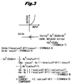
- FIG. 3 is a diagram explaining operational principles of the photoelectric converter according to the present invention.
- the light receiver 8 is a photodiode showing the non-linearity characteristic between the input light signal and the output electric signal.
- the input and output characteristic of the light receiver 8 is approximated by a secondary curve.
- the angular velocity of COS ⁇ eT of the mixed light signal is so large that it cannot be covered by frequency characteristics of the light receiver 8 (FIG. 1) and therefore a direct current having an amplitude of (1/2) Ae 2 appears in the first term.
- the angular velocities of COS( ⁇ e+ ⁇ c)T and COS( ⁇ e- ⁇ c)T are so large that they cannot be covered by the frequency characteristics of the light receiver 8 and therefore the envelope Ae ⁇ Ac[1+KCOS( ⁇ mT+ ⁇ 1) of the carrier_wave COS( ⁇ e+ ⁇ c)T and the envelope Ae ⁇ Ac[1+KCOS( ⁇ mT+ ⁇ 1) of the carrier wave COS( ⁇ e- ⁇ c)T appear in the second and third terms.
- the band-pass filter BPF1 which has received the output Ea from the amplifier 9 is adapted to extract only sine waves of the above marker signal Em having an angular velocity ⁇ m.
- the electric signal which has passed through the band-pass filter BPF1 is a signal which is approximated by the above Ea is represented by the formula (10).
- the output from the mixer MIX1 contains two components COS(2 ⁇ 1T+ ⁇ 1) and COS ⁇ as main components.
- the output is normalized so that its amplitude is 1.
- the low-pass filter PF1 which has received the above two components is adapted to allow the signal having only the component COS ⁇ 1 to pass.
- the signal having the component COS ⁇ 1 is a signal with a level approximated by a direct current and its range of the level depends upon the delay time Td1 in the wavelength ⁇ 1 of the light signal from the light source board CH1.
- the comparator R1 receives the signal having the level ( COS ⁇ 1 )and compares the level of the signal with a predetermined reference voltage Vr1.
- the comparator R1 if the level of the signal received by the comparator R1 is lower than the reference voltage Vr1 (i.e., at a point "a" in FIG.
- the temperature controlling circuit TEC1 is adapted to send a control signal to the temperature controlling circuit TEC1 in order to decrease an oscillating frequency of the light source LD1 and to control so that the wavelength ⁇ 1 is increased by ⁇ .As a result, the delay time Td1 is increased by ⁇ Td and the value of the delay time moves to a point "c" as shown in FIG. 2(b).
- the comparator R1 if the level of the signal received by the comparator R1 is higher than the reference voltage Vr1 (i.e., at a point "b" in FIG.
- the wavelength of the light signal output from the light source LD1 of the light source board CH1 is automatically controlled by the wavelength ⁇ 1.
- the wavelength of each of the light sources (LD2 to LDn) is automatically controlled (to be ⁇ 2 to ⁇ n).
- the configurations provided with the circulator 21 (FIG. 2) and the CFBG 22 (FIG. 2) are used as the dispersion generator 3 (FIG. 1), however, the present invention is not limited to this configuration.
- the equipment by using a device having a wavelength dispersion characteristic, for example, a dispersion compensating fiber used for compensating the dispersion of the wavelength occurring in the optical communication network.
- a device having a wavelength dispersion characteristic for example, a dispersion compensating fiber used for compensating the dispersion of the wavelength occurring in the optical communication network.
- the light receiver 8 (FIG. 1) is used which has input and output characteristics so called "square characteristics" in which an electric signal being changed in proportion to the square of an inputted signal amplitude is outputted.
- the present invention is not limited to the light receiver having the square characteristics, i.e., any device may be employed which is adapted to output a component having the amplitude value Ad ⁇ Ae obtained by multiplying the amplitude Ad of the above-described wavelength-dispersed light signal Ed by the above-described local oscillating amplitude Ae.
- any device having cubic or biquadratic characteristics may be used.
- the wavelength of the light source of the light sources (LD1 to LDn) can be selected, not in a comb-teeth like and desultory manner, but consecutively and arbitrarily.
- the error can be reduced readily.
- the Mach-Zehnder filter used in the conventional embodiment is not employed in the embodiment of the present invention, the control on temperatures is not required for dithering, resulting in the elimination of adverse effects caused by changes in temperatures on peripheral devices.
- the amplitude of the light signal received by the light receiver is substantially amplified optically by the local oscillating light signal Ee, the accuracy in the control on the wavelength can be greatly improved.
- FIG. 4 is a schematic block diagram showing stabilizing equipment 10 for a light source device 11 used in the WDM (Wavelength Division Multiplexing) optical communication according to a second embodiment of the present invention.
- WDM Widelength Division Multiplexing
- a light source device 11 for a WDM optical communication of the present invention is comprised of n-pieces of light source boards CH1 to CHn, a light switch 1, an external modulator 2, a dispersion generator 3, a photoelectric converter 24, a phase difference detector P and a comparator R. Only configurations being different from those in the first embodiment are described below.
- the photoelectric converter 24 is provided with a light receiver 8, a coupler B, a local oscillating light source 25, a temperature adjusting circuit 26, an output power adjusting circuit 27 and a terminating light receiver 28.
- the temperature adjusting circuit 26 and the output power adjusting circuit 27 are adapted to compensate changes caused by temperatures in the output from the local oscillating light source 25.
- the laser diode is used as the local oscillating light source 5 (FIG. 1) to monitor the back-light of the photodiode.
- a light filter and a terminating light receiver 28 are mounted at the terminating point of the coupler B.
- the output light Ee is monitored by the light filter and the terminating light receiver 28 and its output voltage is fed back to the temperature adjusting circuit 26 and the output power adjusting circuit 27. Configurations and operations other than described above are the same as those in the first embodiment and their descriptions are omitted accordingly.
- the following effects are produced by mounting the terminating light receiver 28 at the terminating point of the coupler B adapted to directly monitor the output light from the local oscillating light source 5 and to feed it back to the temperature adjusting circuit 26 and the output power adjusting circuit 27.
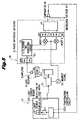
- FIG. 5 is a schematic block diagram showing stabilizing equipment for a light source used in the WDM (Wavelength Division Multiplexing) optical communication according to a third embodiment of the present invention
- the amplitude D is changed due to temperature changes or the like, this change directly appears as changes in the amplitude of the output COS ⁇ 1 . That is, since the output of the comparator R1 is changed due to changes in the amplitude at the external modulator 2 (FIG. 1), the dispersion generator 3 (FIG. 1) and the photoelectric converter 4 (FIG.
- the phase difference detector 31 in order to remove the shortcoming and to detect the phase difference only, is provided with a ⁇ /2 hybrid two-branching circuit and two mixers A and B, which enables the phase difference only to be detected without depending upon the amplitude of the input signal.
- stabilizing equipment 10 for a light source device 11 used in the WDM (Wavelength Division Multiplexing) optical communication is comprised of a light source board CH1, an external modulator 2, a light receiver 8, an amplifier 9, a phase difference detector 31 and a comparator R1.
- the light source board CH1 is a section constituting one channel used to produce a light signal.
- the light source board is provided with a light source LD1 and a coupler A1.
- the light source LD1 is a laser diode to oscillate light with the wavelength ⁇ 1,i.e., a section to output modulated light for optical communication.
- the temperature controlling circuit TEC1 is adapted to change the oscillating frequency of the light source LD1 in accordance with a control signal.
- the coupler A1 is used to separate a part of the modulated light Ec from the light source board CH1 and to take it out.
- the external modulator 2 is used to receive a part of the modulated light Ec of a channel formed by the light source board CH1 and to perform amplitude-modulation of the light by using a marker signal Em having a predetermined angular velocity set arbitrarily.
- the external modulator 2 is composed of, for example, a single crystal of lithium niobate or the like.
- the dispersion generator 3 is adapted to receive the amplitude-modulated light signal Eo from the external modulator 2 and to perform wavelength-dispersion by using, for example, a fiber for compensating the dispersion, chirped fiber black gratings (CFBG) or the like.
- CFBG chirped fiber black gratings
- the light receiver 8 is composed of a photodiode adapted to receive the wavelength-dispersed light signal Ed to be outputted from the dispersion generator 3 and to convert this light signal to electrical signals.
- the amplifier 9 is used to amplify the electrical signals converted by the light receiver.
- the phase difference detector 31 is a section to get a control signal used to stabilize the oscillating frequency of the above light source LD1.
- the phase difference detector 31 is provided with a band-pass filter BPF1, the ⁇ /2 hybrid two-branching circuit 32, the mixers A and B and an analog arithmetic unit 33.
- the band-pass filter BPF1 is a filter adapted to allow a signal having a frequency band of the marker signal, i.e., a predetermined frequency band of COS ⁇ mT to pass therethrough.
- the ⁇ /2 hybrid two-branching circuit 32 is a circuit adapted to receive a signal having the frequency band of the marker signal, i.e., an input having the band COS ⁇ mT to output two signals being different by ⁇ /2 in their phase from each other, one having a band of COS ⁇ mT and the other having a band of SIN ⁇ mT .
- the branching circuit is ordinarily composed of a coaxial cable and a strip line.
- the mixers A and B are multipliers used to multiply two signals.
- the low-pass filters LPF1 and LPF2 are filters adapted to receive the output from the mixers A and B respectively and to output low frequency band components only.
- the analog arithmetic unit 33 is a circuit adapted to receive outputs from the low-pass filters PLF1 and PLF2 and to perform a designated arithmetic operation. The arithmetic operation is later described in detail.
- the comparator R1 is a section adapted to receive the output from the phase difference detector 31 and to compare it with the reference voltage Vr1 predetermined by the CH1. The result of the comparison is fed back to the temperature controlling circuit TEC1 as a control signal.
- the light source LD1 of the light source board CH1 is adapted to oscillate the modulated light Ec having the wavelength ⁇ 1.A part of the modulated light Ec is separated by the coupler A1 and then is transmitted to the external modulator.
- the external modulator 2 is used to perform amplitude modulation of the modulated light Ec by using the marker signal Em and then to feed the amplitude-modulated light signal Eo to the dispersion generator 3.
- the dispersion generator 3 is used to perform wavelength-dispersion of the amplitude-modulated light signal Eo.
- the modulated light Ec and the marker signal Em are represented by the following formula.
- the modulated light signal Eo is expressed by the following formula when the formulas (1) and (2) are incorporated.
- Eo Ac(1+K ⁇ COS ⁇ mT)COS ⁇ cT where, Ac represents the amplitude of the modulated light Ec, Am represents the amplitude of the marker signal Em, ⁇ c represents the angular velocity of the modulated light Ec, ⁇ m represents the angular velocity of the marker signal Em, T represents time and K represents the modulation rate.
- the light signal Eo represented by the formula (3) is fed to the dispersion generator 3. Configurations and operational principles of the dispersion generator 3 of the third embodiment are the same as those disclosed in the first embodiment and their descriptions are omitted accordingly.
- the light signal Eo represented by the formula (3) is converted by the dispersion generator 3 to the signal Ed, the wavelength of which is dispersed, represented by the following formula.
- Ed Ac[1+K ⁇ COS( ⁇ mT+ ⁇ 1)]COS ⁇ cT
- ⁇ 1 represents an absolute phase caused by delay time occurring in the dispersion generator 3. That is, because the wavelength of light from the light source board is ⁇ 1, ⁇ 1 is given by the following formula.
- ⁇ 1 2 ⁇ Td/ ⁇ 1 This means that the envelop is delayed by the absolute phase ⁇ 1 caused by the delay time Td.
- the light signal Ed the wavelength of which is dispersed by the dispersion generator 3, represented by the formula (4) is fed to the light receiver 8.
- the angular velocity of COS ⁇ cT is so large that it cannot be covered by the frequency characteristics of the light receiver 8 and therefore only the envelope Ac[1+KCOS( ⁇ mT+ ⁇ 1) of the carrier_wave appears.
- Es direct current component + C ⁇ COS( ⁇ mT+ ⁇ 1) where, C is a constant which changes in proportion to the amplitude Ae ⁇ Ac of the envelop Ae ⁇ Ac[1+K ⁇ COS( ⁇ mT+ ⁇ 1)] .
- the direct current component contained in this output Es is cut by the amplifier 9 and is amplified.
- the amplified light signal Es is passed through the band pass filter BPF1.
- the Ea is fed to the ⁇ /2 hybrid two-branching circuit 32.
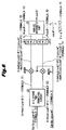
- FIG. 6 is a diagram explaining principles of the third embodiment. Flows of arithmetic operations performed by the ⁇ /2 hybrid two-branching circuit 32 to the analog arithmetic unit 33 are shown in FIG. 6. As shown in FIG. 6,
- the ⁇ /2 hybrid two-branching circuit 32 adapted to receive the signal Ea, which passed through the band pass filter BPF1, represented by the formula 10 outputs the following two signals being different by ⁇ /2 phase from each other
- Eh H ⁇ SIN( ⁇ mT+ ⁇ 1)
- Eh H ⁇ COS( ⁇ mT+ ⁇ 1)
- the signal Eh represented by the formula (11) is multiplied by the marker signal Em represented by the formula (2) by the mixer A, to be converted as follows.
- X (Am ⁇ H/2)[SIN(2 ⁇ mT+ ⁇ 1)+SIN ⁇ 1]
- the signal Ei represented by the formula (12) is multiplied by the above marker signal Em by the mixer B, to be converted as follows.
- Y (Am ⁇ H/2)[COS(2 ⁇ mT+ ⁇ 1)+COS ⁇ 1]
- the low-pass filter LPF1 adapted to receive the signal X represented by the formula (13) outputs low frequency components given by the following equation.
- X L F ⁇ SIN ⁇ 1
- the low-pass filter LPF2 adapted to receive the signal Y represented by the formula (14) outputs low frequency components given by the following equation.
- Y L F ⁇ COS ⁇ 1
- the analog arithmetic unit 33 is used to perform arithmetic operations of the following functional formula showing a relation between the signal X L represented by the formula (15) and the signal Y L represented by the formula (16).
- F (X L 2 +Y L 2 ) 1/2
- the comparator R1 is used to receive this level signal COS ⁇ 1 and compare it with the reference voltage Vr1.
- the oscillating frequency of the light source LD1 is decreased by supplying a control signal to the temperature control circuit TEC1 so that the wavelength ⁇ 1 is increased by ⁇ .As a result, the delay time Td1 is increased by ⁇ Td and the value moves to point "c".
- the level of the signal received by the comparator R1 is higher than the reference voltage Vr1 (point "b" of (b) in FIG. 2)
- the oscillating frequency of the light source LD1 is increased by supplying a control signal to the temperature control circuit TEC1 so that the wavelength ⁇ 1 is decreased by ⁇ ⁇ .As a result, the delay time Td1 is decreased by ⁇ Td and the value moves to point "c".
- the wavelength of the light signal output of the light source LD1 of the light source board CH1 is automatically controlled so as to be ⁇ 1.
- the equipment of the present invention may be so configured that a plurality of light sources CH1 to CHn is provided and that one channel out of n-pieces of channels by light switch is selected and the reference voltage to be applied to the comparator R1 is switched for every selected channel.
- the photoelectric converter may be used in any embodiment.
- the frequency stabilizing equipment may be used in not only the wavelength division multiplexing system but also in various optical communication system.
Landscapes
- Physics & Mathematics (AREA)
- Electromagnetism (AREA)
- Engineering & Computer Science (AREA)
- Computer Networks & Wireless Communication (AREA)
- Signal Processing (AREA)
- Nonlinear Science (AREA)
- Optical Communication System (AREA)
- Semiconductor Lasers (AREA)
Applications Claiming Priority (2)
| Application Number | Priority Date | Filing Date | Title |
|---|---|---|---|
| JP8845999 | 1999-03-30 | ||
| JP08845999A JP4008617B2 (ja) | 1999-03-30 | 1999-03-30 | 光源の周波数安定化装置 |
Publications (2)
| Publication Number | Publication Date |
|---|---|
| EP1041748A2 true EP1041748A2 (fr) | 2000-10-04 |
| EP1041748A3 EP1041748A3 (fr) | 2004-06-09 |
Family
ID=13943379
Family Applications (1)
| Application Number | Title | Priority Date | Filing Date |
|---|---|---|---|
| EP00106113A Withdrawn EP1041748A3 (fr) | 1999-03-30 | 2000-03-21 | Stabilisateur de fréquence pour une source lumineuse pour la communication optique |
Country Status (3)
| Country | Link |
|---|---|
| US (1) | US6556328B1 (fr) |
| EP (1) | EP1041748A3 (fr) |
| JP (1) | JP4008617B2 (fr) |
Families Citing this family (7)
| Publication number | Priority date | Publication date | Assignee | Title |
|---|---|---|---|---|
| JP3721062B2 (ja) * | 2000-08-30 | 2005-11-30 | 日本電信電話株式会社 | 光送信機 |
| JP3737383B2 (ja) * | 2001-05-21 | 2006-01-18 | ユーディナデバイス株式会社 | 半導体レーザモジュール試験装置および半導体レーザモジュール試験方法 |
| KR100552091B1 (ko) * | 2002-10-04 | 2006-02-14 | 광운대학교 산학협력단 | 초고밀도 파장분할다중화된 광채널에 대한 광주파수제어장치 |
| US8781327B2 (en) * | 2010-07-09 | 2014-07-15 | Futurewei Technologies, Inc. | Use of multiple shared wavelength lockers to stabilize transponders in a wavelength division multiplexing (WDM) network |
| JP5962455B2 (ja) * | 2012-11-21 | 2016-08-03 | 富士通株式会社 | 光伝送装置、ノード装置、光伝送方法および光伝送システム |
| JP2017147622A (ja) * | 2016-02-17 | 2017-08-24 | 富士通オプティカルコンポーネンツ株式会社 | 光送信機、及び制御方法 |
| US10211943B2 (en) * | 2017-01-20 | 2019-02-19 | Adva Optical Networking Se | Method and apparatus for managing a frequency spectrum in a wavelength division multiplexing network |
Family Cites Families (8)
| Publication number | Priority date | Publication date | Assignee | Title |
|---|---|---|---|---|
| US4912716A (en) * | 1988-11-16 | 1990-03-27 | Spectra-Physics, Inc. | Method and apparatus for frequency modulation stabilization of a laser |
| US5204640A (en) * | 1992-02-10 | 1993-04-20 | California Institute Of Technology | Widely tunable oscillator stabilization using analog fiber optic delay line |
| JP2772605B2 (ja) * | 1992-10-15 | 1998-07-02 | 国際電信電話株式会社 | 光周波数多重キャリヤ制御装置 |
| DE4317667A1 (de) * | 1993-05-27 | 1994-12-01 | Sel Alcatel Ag | Aktiv modengekoppelter Faserlaser |
| JP3234429B2 (ja) * | 1995-01-17 | 2001-12-04 | 日本電信電話株式会社 | モード同期レーザの動作安定化装置 |
| US6111681A (en) * | 1996-02-23 | 2000-08-29 | Ciena Corporation | WDM optical communication systems with wavelength-stabilized optical selectors |
| JP3724894B2 (ja) * | 1996-10-24 | 2005-12-07 | 富士通株式会社 | 光送信機 |
| US6151481A (en) * | 1998-03-13 | 2000-11-21 | Lockheed Martin Corporation | Combiner with phase and delay correction |
-
1999
- 1999-03-30 JP JP08845999A patent/JP4008617B2/ja not_active Expired - Fee Related
-
2000
- 2000-03-21 EP EP00106113A patent/EP1041748A3/fr not_active Withdrawn
- 2000-03-22 US US09/533,358 patent/US6556328B1/en not_active Expired - Fee Related
Also Published As
| Publication number | Publication date |
|---|---|
| JP4008617B2 (ja) | 2007-11-14 |
| JP2000286500A (ja) | 2000-10-13 |
| US6556328B1 (en) | 2003-04-29 |
| EP1041748A3 (fr) | 2004-06-09 |
Similar Documents
| Publication | Publication Date | Title |
|---|---|---|
| US6370169B1 (en) | Method and apparatus for controlling optical wavelength based on optical frequency pulling | |
| EP1391064B8 (fr) | Controle de longueur d'onde par modulation a vibration et retroaction | |
| US6178036B1 (en) | Opto-electronic devices and systems based on brillouin selective sideband amplification | |
| US6421151B1 (en) | Method and arrangement for stabilizing wavelength of multi-channel optical transmission systems | |
| US7245833B1 (en) | Photonic channelized RF receiver employing dense wavelength division multiplexing | |
| US6556327B1 (en) | Signal converter, optical transmitter and optical fiber transmission system | |
| EP1195927A2 (fr) | Système et procédé pour la détection optique hétérodyne d'un signal optique avec présélection optique ajustée pour poursuivre avec précision un signal d'oscillateur local | |
| CN1926791B (zh) | 载波残留型信号的生成方法及其装置 | |
| US6807321B2 (en) | Apparatus and method for measurement and adaptive control of polarization mode dispersion in optical fiber transmission systems | |
| US20020171894A1 (en) | Optical linearizer for fiber communications | |
| US20030165286A1 (en) | Wavelength division multiplex transmission system | |
| US6088144A (en) | Detection of frequency-modulated tones in electromagnetic signals | |
| US5390017A (en) | Optical network analyzer for measuring the amplitude characteristics and group delay time dispersion characteristics of an optical circuit device | |
| EP3321720B1 (fr) | Dispositif de filtre d'interférence optique, en particulier pour un dispositif de verrouillage de longueur d'onde optique | |
| CN106027152A (zh) | 一种基于马赫增德尔调制器8倍频产生120GHz毫米波的方法 | |
| EP4123257B1 (fr) | Réglage de phase et stabilisation de phase de multiples interféromètres | |
| US8611744B2 (en) | Monitoring system employing carrier recovery | |
| US6556328B1 (en) | Frequency stabilizing equipment for optical communication light source | |
| US6493125B1 (en) | Apparatus for stabilizing light source frequency | |
| CN113612543A (zh) | 微波光子单光频率梳注入锁定的信道化接收装置及方法 | |
| US7068944B2 (en) | Multi-function optical performance monitor | |
| EP0723343B1 (fr) | Distribution et réception des signaux de référence de longueur d'onde dans un réseau optique et multicanal | |
| JP3699854B2 (ja) | 光源の周波数安定化装置 | |
| EP1783930B1 (fr) | Modulateur optique de type fsk | |
| JPH01164135A (ja) | 光周波数分割多重伝送方式における半導体レーザの発振周波数安定化方法 |
Legal Events
| Date | Code | Title | Description |
|---|---|---|---|
| PUAI | Public reference made under article 153(3) epc to a published international application that has entered the european phase |
Free format text: ORIGINAL CODE: 0009012 |
|
| AK | Designated contracting states |
Kind code of ref document: A2 Designated state(s): AT BE CH CY DE DK ES FI FR GB GR IE IT LI LU MC NL PT SE |
|
| AX | Request for extension of the european patent |
Free format text: AL;LT;LV;MK;RO;SI |
|
| RIC1 | Information provided on ipc code assigned before grant |
Ipc: 7H 01S 3/13 B Ipc: 7H 04B 10/155 B Ipc: 7H 04B 10/145 A |
|
| PUAL | Search report despatched |
Free format text: ORIGINAL CODE: 0009013 |
|
| AK | Designated contracting states |
Kind code of ref document: A3 Designated state(s): AT BE CH CY DE DK ES FI FR GB GR IE IT LI LU MC NL PT SE |
|
| AX | Request for extension of the european patent |
Extension state: AL LT LV MK RO SI |
|
| STAA | Information on the status of an ep patent application or granted ep patent |
Free format text: STATUS: THE APPLICATION IS DEEMED TO BE WITHDRAWN |
|
| AKX | Designation fees paid | ||
| REG | Reference to a national code |
Ref country code: DE Ref legal event code: 8566 |
|
| 18D | Application deemed to be withdrawn |
Effective date: 20040901 |