EP1042865B1 - Procede de commande reference par impulsion et destine a une amplification de puissance accrue d'un signal module par impulsion - Google Patents
Procede de commande reference par impulsion et destine a une amplification de puissance accrue d'un signal module par impulsion Download PDFInfo
- Publication number
- EP1042865B1 EP1042865B1 EP98910630A EP98910630A EP1042865B1 EP 1042865 B1 EP1042865 B1 EP 1042865B1 EP 98910630 A EP98910630 A EP 98910630A EP 98910630 A EP98910630 A EP 98910630A EP 1042865 B1 EP1042865 B1 EP 1042865B1
- Authority
- EP
- European Patent Office
- Prior art keywords
- pulse
- error
- correction unit
- switching power
- signal
- Prior art date
- Legal status (The legal status is an assumption and is not a legal conclusion. Google has not performed a legal analysis and makes no representation as to the accuracy of the status listed.)
- Expired - Lifetime
Links
- 230000003321 amplification Effects 0.000 title claims abstract description 20
- 238000003199 nucleic acid amplification method Methods 0.000 title claims abstract description 20
- 238000000034 method Methods 0.000 title claims description 30
- 238000012937 correction Methods 0.000 claims abstract description 40
- 238000006243 chemical reaction Methods 0.000 claims abstract description 27
- 238000007493 shaping process Methods 0.000 claims abstract description 12
- 230000000694 effects Effects 0.000 claims abstract description 10
- 230000001934 delay Effects 0.000 claims abstract description 9
- 230000008859 change Effects 0.000 claims description 3
- 230000010354 integration Effects 0.000 claims description 2
- 230000004044 response Effects 0.000 description 6
- 238000013461 design Methods 0.000 description 5
- 238000012546 transfer Methods 0.000 description 5
- 230000006872 improvement Effects 0.000 description 4
- 238000013459 approach Methods 0.000 description 3
- 230000009977 dual effect Effects 0.000 description 3
- 230000035945 sensitivity Effects 0.000 description 3
- 238000010586 diagram Methods 0.000 description 2
- 238000005457 optimization Methods 0.000 description 2
- 238000004088 simulation Methods 0.000 description 2
- 238000012935 Averaging Methods 0.000 description 1
- 238000007792 addition Methods 0.000 description 1
- 239000011162 core material Substances 0.000 description 1
- 230000008030 elimination Effects 0.000 description 1
- 238000003379 elimination reaction Methods 0.000 description 1
- 238000011835 investigation Methods 0.000 description 1
- 238000012886 linear function Methods 0.000 description 1
- 239000013643 reference control Substances 0.000 description 1
- 230000005236 sound signal Effects 0.000 description 1
- 230000007704 transition Effects 0.000 description 1
Images



Classifications
-
- H—ELECTRICITY
- H03—ELECTRONIC CIRCUITRY
- H03F—AMPLIFIERS
- H03F3/00—Amplifiers with only discharge tubes or only semiconductor devices as amplifying elements
- H03F3/20—Power amplifiers, e.g. Class B amplifiers, Class C amplifiers
- H03F3/21—Power amplifiers, e.g. Class B amplifiers, Class C amplifiers with semiconductor devices only
- H03F3/217—Class D power amplifiers; Switching amplifiers
Definitions
- This invention relates to power amplification of pulse modulated signals by a switching power stage.
- the invention may advantageously be used for improved conversion of a digital signal directly to analog power.
- Applications are direct digital audio power conversion and general DC-DC or DC-AC power conversion systems controlled from the digital domain.
- the advantages of power amplification based on a switching power stage are well known.
- the high efficiency provides several advantages, in terms of minimal weight and volume, higher power handling capability and improved reliability.
- the fundamental elements in switching power amplification are the modulator, the switching power stage and the demodulation filter to reconstitute the modulated signal.
- the non-linearity of the switching power stage presents a significant impediment to maintain the modulator performance throughout the subsequent power conversion by a switching power stage. This problem is fundamental and independent on the use of analog modulation as analog PWM, or digital modulation as direct digital PCM-PWM conversion.
- the primary objective of the present invention is to enable improved power amplification of a pulse modulated signal, where all error sources related to the power stage and demodulation filter are eliminated, such that the modulator performance can be maintained throughout the subsequent elements all the way to the output.
- Another objective of the invention is to provide a practical digital PCM - power conversion system, that is insensitive to power stage non-linearity, perturbation on the power supply and any other non-ideal elements.
- the objectives of the invention are achieved by the introduction of a correction unit in-between the pulse modulator and the switching power amplification stage.
- the correction unit provides compensation by means of pulse re-timing on the pulse edges, said re-timing controlled to have a "predistorting" effect, such that the resulting switching power stage output is free from distortion, noise or any other undesired contribution.
- one preferred embodiment of the invention is particular in that pulse re-retiming in the correction unit is a linear function of an error signal input. This is advantageous in that the resulting control system is linear, whereby system design and optimization is simplified and the performance improvement controllable.
- the pulse reference control system comprises the following fundamental elements:
- the invention includes various embodiments regarding actual realization of the control function within the correction unit. According to claims 6-10, the invention includes various advantageous embodiments concerning improved digital - analog power conversion suitable for audio power amplification.
- the invention is a fundamentally new control method for improved amplification of a pulse modulated input signal.
- the application range is extremely broad in that the invention can be used with any pulse-modulated input, modulated in the analog or digital domain, and feed any load where a pulsed power signal of controllable quality is needed.
- the principle of the invention may realize perfect reproduction of the pulsed reference such that the output is a constant times the input, independent on any disturbances that is introduced during power conversion.
- Pulse Timing Errors arise from:
- Pulse Amplitude Errors mainly arise from:
- the demodulation filter errors may introduce further distortion, since magnetic core materials are not ideal.
- the filter increases the total output impedance. Accordingly, changes in load impedance will distort the frequency response.
- Fig. 1 shows a method, well known in the art, to realize power amplification based on analog pulse modulation techniques.
- the modulator output feeds a switching power stage, the output of which is demodulated and feed to the load.
- a linear control system referenced to the analog input serves to minimize the errors within the power conversion, such that the effects of the above mentioned errors can be minimized.
- a digital input requires a separate D/A converter to generate the analog input that serves as input to the control system.
- Fig. 2 illustrates the simplified and desirable system for direct digital to analog power conversion using digital pulse modulation techniques, also well known in prior art.
- the application of error feedback control is complicated in that an analog/digital converter would be needed to enable comparison with the digital reference source. This compromises both performance and complexity and renders the method impractical.
- the new principle of the invention is shown by the general block diagram in Fig. 3.
- the modulator is feed to a correction unit that serves to correct or "predistort" the pulse modulated signal ⁇ r to generate the compensated pulse signal ⁇ c , such that the said non-ideal behavior within the subsequent power conversion and demodulation are eliminated.
- This is carried out by means of intelligent pulse edge delays on each of the pulse edges, controlled by an input control signal ⁇ e to the correction unit.
- the method will henceforth be referenced to as Pulse Edge Delay Error Correction (PEDEC).
- the invention is a fundamentally new control method for improved amplification of a pulse modulated input signal.
- the application range is broad in that the invention can be used with any pulse-modulated input, modulated in the analog or digital domain, and feed any load where a pulsed power signal of controllable quality is needed.
- the invention relies on two fundamental facts:
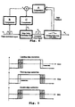
- the edge correction may be implemented using single-sided or double-sided edge delay correction, as shown conceptually in Fig. 5.
- the choice of single or double edge correction is independent of the type of modulation method.
- the control of both edges leads to efficient correction and furthermore has simple implementation strategies. Subsequently, the following description of this aspect of the invention will focus on double edge correction.
- the dual input pulse referenced feedback control system comprises:
- the correction unit may be realized by various linear and also non-linear methods.
- This preferred linear control function is advantageous in that it simplifies controller design and provides controllable performance improvements compared to e.g. the implementation of a non-linear control function.
- a preferred embodiment of the invention is particular in that the implementation of a double-sided correction unit that implements (4) is simple.
- the method is shown in Fig. 6.
- the linear control function is realized by a limited integration of the reference v r , thus generating the signal v i .
- a comparison between the modified reference with the control signal v e caused the pulse edges to be re-timed. From Fig. 6 in follows that:
- ( ⁇ ) indicates the corrected variable after passing the PEDEC unit. It is assumed that all pulse amplitudes are normalized to unity.
- Fig. 7 shows a preferred implementation of the double-sided edge correction method. The method is very simple and straightforward.
- the pulses should have a certain minimal width.
- t 0 is preferably on order of magnitude or more lower that t s .
- the invention includes several embodiments regarding the application of the invention specifically in digital to analog power conversion.
- One preferred embodiment is the system shown in Fig. 8.
- PEDEC in combination with one of the high performance digital pulse width modulation methods (PCM-PWM methods) that are known to the art, the signal will remain digital or pulsed throughout the main audio chain.
- No analog modulator or carrier generator is needed as with analog pulse modulation, since the system is controlled exclusively by the digital modulator.
- the state feedback is a voltage feedback from the switching power stage output ⁇ p .
- the feedback path compensator is a simple attenuation, and the compensator block C(s) is a linear filter.
- the system introduces a very powerful and flexible control of system performance.
- the preferred linear control function provides great flexibility in performance optimization.
- An example of PEDEC control system design is specified in the following.
- the compensator is defined in the linear model of the system as shown in Fig. 9.
- the PEDEC unit has been replaced by its equivalent linear gain and the resulting system has been redrawn to emphasize the dual input character of the PEDEC based digital to power conversion system.
- the specified compensator provides sufficient flexibility to optimize the performance to various characteristics.
- the compensator DC gain K C is optimized to yield the desired loop bandwidth.
- a bandwidth of 6-8 times target bandwidth is a good compromise between efficiency and error correction capability.
- Fig. 12 shows Bode plots for each component and the resulting loop transfer function.
- Example of frequency normalized parameters Parameter Value Comment k PEDEC 0.2 Equivalent PEDEC unit gain.
- the gain of the system is controlled by the A-block, and with the given example embodiment, the PEDEC control system will force the system gain to be constant within the target bandwidth. This stabilizes both system gain and the frequency response.
- the resulting system response is constituted of two contributions, since the reference has two inputs in the loop.
- the system transfer function is:
- Fig. 13 shows the resulting Bode plots for the closed system, consisting of two contributions forming the loop response and a total system response with the demodulation filter.
- the constant gain characteristic of the loop caused by K K P .
- the demodulation filter exclusively determines the response of the system.
- Fig. 10 and Fig. 11 are characterized by using different compensator and reference shaping blocks.
- the embodiment in Fig. 10 is preferably based on a first order characteristic in both the reference shaping block R(s) and the feedback compensator A(s).
- the advantages in the demodulation of both reference and feedback signal are minimized noise within the control system and furthermore lower bandwidth requirements for the feedback compensator.
- the embodiment in Fig. 11 is based on a global feedback source such that demodulation filter errors are included within the loop and also corrected for. This requires a second order reference shaper for optimal error estimation.
- Fig. 14 The correction effects towards pulse timing errors (PTE) is shown in Fig. 14, where THD for the open loop system and three PEDEC controller configurations have been investigated at the worst case signal frequency. Clearly, the controller considerably reduces the effects of this particular error source. Furthermore, adjusting the compensator gain K C can control the improvements. In this particular situation the distortion is reduced 20dB - 30dB.
- Fig. 15 shows an investigation of PAE with a severe power supply perturbation of 10 Vpp. Top figure visualizes the clear intermodulation between power supply and signal. Bottom figure shows how the PEDEC controller eliminates this effect such that the intermodulation is no more visible in the time domain. The intermodulation distortion is reduced more than 40dB compared to the open loop case, as predicted by the sensitivity function in theory.
Landscapes
- Engineering & Computer Science (AREA)
- Power Engineering (AREA)
- Amplifiers (AREA)
- Amplitude Modulation (AREA)
- Stabilization Of Oscillater, Synchronisation, Frequency Synthesizers (AREA)
- Power Conversion In General (AREA)
Claims (11)
- Méthode de correction pour toute source de non linéarité et de bruit introduite dans l'amplification de puissance d'un signal modulé par impulsion, caractérisée par l'introduction d'une unité de correction entre le modulateur d'impulsions et l'étage d'amplification de la puissance de commutation, ladite unité de correction introduisant des retards au niveau des flancs d'impulsion, commandés pour qu'ils aient un effet de compensation.
- Méthode selon la revendication 1, caractérisée en ce que la correction de retard du flanc d'impulsion est effectuée au niveau du flanc antérieur, du flanc arrière, ou au niveau des deux flancs du signal entrant modulé par impulsion.
- Méthode selon les revendications 1 et 2, caractérisée en ce que la correction est effectuée par une modification effective de la largeur d'impulsion Δtw dans chaque cycle de commutation, commandée en tant que fonction de régulation linéaire d'un signal d'erreur ve à l'unité de correction, de sorte qu'une relation linéaire Δtw = kw.ve est établie.
- Appareil pour l'application de la méthode selon l'une quelconque des revendications 1 à 3, caractérisé en ce que l'appareil comprend :un terminal d'entrée qui réceptionne un signal modulé par impulsion,une unité de correction avec des moyens pour réguler le retard des flancs d'impulsion individuels,un bloc de réaction d'état avec une compensation par le bloc d'étage de puissance,un bloc optionnel de formation des impulsions de référence,une unité de soustraction pour prendre la dérivée de l'information d'erreur, etun compensateur pour mettre en forme ladite erreur et pour alimenter l'unité de correction avec ladite erreur mise en forme.
- Appareil selon la revendication 4, caractérisé en ce que l'implémentation de la correction de flanc en deux endroits est réalisée grâce à une intégration limitée de la référence pulsée afin de générer un nouveau signal vi, de sorte qu'une comparaison entre vi et le signal d'erreur ve à l'intérieur de l'unité de correction réalise une fonction de régulation linéaire sous la forme de Δtw = kw -ve.
- Méthode selon l'une quelconque des revendications 1 à 3 ou appareil selon les revendications 4 et 5, où l'entrée de référence est modulée par modulation de la largeur d'impulsion.
- Méthode selon l'une quelconque des revendications 1 à 3 ou appareil selon les revendications 4 et 5, pour la réalisation d'un système général numérique MIC - de conversion de la puissance analogique, ayant fait ses preuves.
- Appareil selon l'une quelconque des revendications 4 à 7, caractérisé en ce que la réaction d'état est la tension de sortie locale de la puissance de commutation vp, et en ce que le bloc de formation des impulsions de référence est d'unité.
- Appareil selon l'une quelconque des revendications 4 à 7 utilisé en tant qu'amplificateur de puissance, caractérisé en ce que la réaction d'état est la puissance utile de commutation locale, en ce que la compensation de la réaction est un filtre de premier ordre, et en ce que le bloc de formation des impulsions de référence forme de la même manière un système de premier ordre.
- Appareil selon l'une quelconque des revendications 4 à 7 utilisé en tant qu'amplificateur de puissance, caractérisé en ce que la réaction d'état est le rendement de sortie global de l'amplificateur, en ce que le bloc de formation des impulsions de référence est un filtre de second ordre, et en ce que la compensation du chemin de réaction est une atténuation constante.
- Méthode selon l'une quelconque des revendications 1 à 3 ou selon l'une quelconque des revendications 4 à 10, caractérisée en ce que la puissance utile de l'étage de la puissance de commutation commande directement un haut-parleur ou une autre charge avec des impulsions directement à partir de l'étage de la puissance de commutation.
Applications Claiming Priority (3)
| Application Number | Priority Date | Filing Date | Title |
|---|---|---|---|
| DK37597 | 1997-04-02 | ||
| DK37597 | 1997-04-02 | ||
| PCT/DK1998/000133 WO1998044626A2 (fr) | 1997-04-02 | 1998-04-01 | Procede de commande reference par impulsion et destine a une amplification de puissance accrue d'un signal module par impulsion |
Publications (3)
| Publication Number | Publication Date |
|---|---|
| EP1042865A2 EP1042865A2 (fr) | 2000-10-11 |
| EP1042865B1 true EP1042865B1 (fr) | 2004-10-13 |
| EP1042865B8 EP1042865B8 (fr) | 2005-01-19 |
Family
ID=8092799
Family Applications (1)
| Application Number | Title | Priority Date | Filing Date |
|---|---|---|---|
| EP98910630A Expired - Lifetime EP1042865B8 (fr) | 1997-04-02 | 1998-04-01 | Procede de commande reference par impulsion et destine a une amplification de puissance accrue d'un signal module par impulsion |
Country Status (10)
| Country | Link |
|---|---|
| US (1) | US6768779B1 (fr) |
| EP (1) | EP1042865B8 (fr) |
| JP (1) | JP3346581B2 (fr) |
| KR (1) | KR100426422B1 (fr) |
| CN (1) | CN1123116C (fr) |
| AT (1) | ATE279811T1 (fr) |
| AU (1) | AU730339B2 (fr) |
| CA (1) | CA2285355C (fr) |
| DE (1) | DE69827039T2 (fr) |
| WO (1) | WO1998044626A2 (fr) |
Families Citing this family (93)
| Publication number | Priority date | Publication date | Assignee | Title |
|---|---|---|---|---|
| US6362683B1 (en) * | 1999-07-29 | 2002-03-26 | Tripath Technology, Inc. | Break-before-make distortion compensation for a digital amplifier |
| FI107659B (fi) * | 1999-11-26 | 2001-09-14 | Nokia Mobile Phones Ltd | Signaalin laadun parantaminen |
| US6995482B2 (en) | 2000-01-05 | 2006-02-07 | Freescale Semiconductor, Inc. | Switching circuit and method therefor |
| US6441685B1 (en) | 2000-03-17 | 2002-08-27 | Jl Audio, Inc. | Amplifier circuit and method for providing negative feedback thereto |
| AT410152B (de) | 2000-06-07 | 2003-02-25 | Bier Guenther Ing | Verfahren und vorrichtung zur erzeugung einer einem eingangs-datenstrom folgenden wechselspannung |
| EP1184973B1 (fr) * | 2000-08-29 | 2007-06-06 | STMicroelectronics S.r.l. | Equipement amplificateur de puissance |
| SE0003342D0 (sv) * | 2000-09-19 | 2000-09-19 | Bang & Olufsen Powerhouse As | Controlled self-oscillation modulator and power conversion system using such a modulator |
| US6362702B1 (en) | 2000-09-29 | 2002-03-26 | Bang & Olufsen Powerhouse A/S | Controlled self-oscillation modulator and power conversion system using such a modulator |
| US6466087B2 (en) | 2000-12-28 | 2002-10-15 | Nokia Mobile Phones, Ltd. | Method and apparatus providing digital error correction for a class D power stage |
| US7058463B1 (en) | 2000-12-29 | 2006-06-06 | Nokia Corporation | Method and apparatus for implementing a class D driver and speaker system |
| US6462685B1 (en) | 2001-04-05 | 2002-10-08 | Nokia Corporation | Dither signal insertion inversely proportional to signal level in delta-sigma modulators |
| US6504427B2 (en) * | 2001-05-31 | 2003-01-07 | Motorola, Inc. | Switching amplifier having digital correction and method therefor |
| US6404280B1 (en) | 2001-06-01 | 2002-06-11 | Constel Signal Processing Co., Ltd. | Method and system for low-distortion power amplification |
| US6473019B1 (en) | 2001-06-21 | 2002-10-29 | Nokia Corporation | Low capacitance, low kickback noise input stage of a multi-level quantizer with dithering and multi-threshold generation for a multi-bit sigma-delta modulator |
| US6426714B1 (en) | 2001-06-26 | 2002-07-30 | Nokia Corporation | Multi-level quantizer with current mode DEM switch matrices and separate DEM decision logic for a multibit sigma delta modulator |
| US6535155B2 (en) | 2001-06-27 | 2003-03-18 | Nokia Corporation | Method and apparatus for suppressing tones induced by cyclic dynamic element matching (DEM) algorithms |
| US6577258B2 (en) | 2001-10-01 | 2003-06-10 | Nokia Corporation | Adaptive sigma-delta data converter for mobile terminals |
| KR100434236B1 (ko) * | 2001-10-11 | 2004-06-04 | 페어차일드코리아반도체 주식회사 | 모터 제어 구동 회로 |
| CN1195353C (zh) * | 2001-12-03 | 2005-03-30 | 方虎堂 | 脉冲面积调制数字功率处理方法及装置 |
| US7142597B2 (en) * | 2002-09-26 | 2006-11-28 | Freescale Semiconductor, Inc. | Full bridge integral noise shaping for quantization of pulse width modulation signals |
| US6924700B2 (en) | 2002-10-03 | 2005-08-02 | Mitsubishi Denki Kabushiki Kaisha | Class D amplifier |
| JP3776392B2 (ja) * | 2002-10-03 | 2006-05-17 | 三菱電機株式会社 | D級増幅器 |
| DE10393487B3 (de) * | 2002-11-27 | 2007-05-16 | Infineon Technologies Ag | Verfahren und Vorrichtung zur Korrektur von Signalverzerrungen in einer Verstärkereinrichtung |
| DE10255352B3 (de) | 2002-11-27 | 2004-02-12 | Infineon Technologies Ag | Verfahren und Vorrichtung zur Korrektur von Signalverzerrungen in einer Verstärkereinrichtung |
| EP1429454A1 (fr) * | 2002-12-11 | 2004-06-16 | Dialog Semiconductor GmbH | Amplificateur classe D avec compensation du centre de gravité |
| SE0300780D0 (sv) * | 2003-03-24 | 2003-03-24 | Bang & Olufsen Icepower As | Digital pulse width controlled oscillation modulator |
| US7518450B2 (en) * | 2003-04-07 | 2009-04-14 | Nxp B.V. | Digital amplifier |
| US6768437B1 (en) | 2003-06-24 | 2004-07-27 | Nokia Corporation | Switched voltage-mode dither signal generation for a sigma-delta modulator |
| US6922100B2 (en) * | 2003-07-29 | 2005-07-26 | Freescale Semiconductor, Inc. | Method and apparatus for switching amplification having variable sample point and variable order correction |
| JP4561459B2 (ja) * | 2004-04-30 | 2010-10-13 | ヤマハ株式会社 | D級増幅器 |
| EP1653604B1 (fr) | 2004-10-28 | 2009-07-01 | CAMCO Produktions- und Vertriebs GmbH | Amplificateur de puissance à découpage et procédé d'amplification de signaux numériques |
| GB2419757B (en) * | 2004-11-01 | 2008-11-26 | Zetex Plc | A digital amplifier |
| EP1813015B1 (fr) * | 2004-11-12 | 2008-02-13 | Koninklijke Philips Electronics N.V. | Dispositif d'amplification d'un signal d'entree de modulation d'impulsions en largeur |
| TWI282211B (en) * | 2005-01-17 | 2007-06-01 | Realtek Semiconductor Corp | Power amplifier and method for correcting error of output signals thereof |
| DE602006004557D1 (de) * | 2005-01-28 | 2009-02-12 | Nxp Bv | Anordnung zur verstärkung eines pwm-eingangssignals |
| JP4802765B2 (ja) * | 2005-03-18 | 2011-10-26 | ヤマハ株式会社 | D級増幅器 |
| EP1900102A2 (fr) * | 2005-06-27 | 2008-03-19 | Qualcomm Flarion Technologies, Inc. | Procedes et dispositifs pour mettre en place et/ou utiliser des amplificateurs et/ou pour executer differentes operations liees a l'amplification |
| WO2007011012A1 (fr) * | 2005-07-21 | 2007-01-25 | Pioneer Corporation | Dispositif d’amplification de puissance |
| JP4688175B2 (ja) * | 2005-07-21 | 2011-05-25 | パイオニア株式会社 | D級電力増幅装置 |
| CN101228690B (zh) * | 2005-07-29 | 2010-08-18 | 富士通株式会社 | 延迟调整装置 |
| GB2429351B (en) * | 2005-08-17 | 2009-07-08 | Wolfson Microelectronics Plc | Feedback controller for PWM amplifier |
| US7167118B1 (en) * | 2005-12-08 | 2007-01-23 | Cirrus Logic, Inc. | Centered-pulse consecutive edge modulation (CEM) method and apparatus |
| TWI336166B (en) * | 2006-02-20 | 2011-01-11 | Realtek Semiconductor Corp | Digital amplifier and thereof method |
| US7180439B1 (en) * | 2006-03-16 | 2007-02-20 | Analog Devices, Inc. | Multi-path digital power supply controller |
| KR100861797B1 (ko) * | 2006-04-12 | 2008-10-08 | 재단법인서울대학교산학협력재단 | 펄스 변조를 이용한 고효율 선형 전력 증폭기 시스템에서 고조파 성분을 제거하는 장치 |
| US7598714B2 (en) * | 2006-07-12 | 2009-10-06 | Harman International Industries, Incorporated | Amplifier employing interleaved signals for PWM ripple suppression |
| KR100765792B1 (ko) * | 2006-07-28 | 2007-10-12 | 삼성전자주식회사 | 스위칭 파워 앰프에서 에러 보정 방법 및 장치 |
| DE102006055577B4 (de) * | 2006-11-21 | 2014-03-20 | Ihp Gmbh - Innovations For High Performance Microelectronics / Leibniz-Institut Für Innovative Mikroelektronik | Sigma-Delta-Modulator mit Rückkopplung für Leistungsverstärker |
| JP5253413B2 (ja) * | 2006-12-21 | 2013-07-31 | バング アンド オルフセン アイスパワー アクティーゼルスカブ | D級電力段のためのエラー修正システム |
| CN101884167A (zh) * | 2007-12-07 | 2010-11-10 | Nxp股份有限公司 | 包括脉宽脉位调制器的发射机及其方法 |
| US7777562B2 (en) * | 2007-12-20 | 2010-08-17 | Asahi Kasei Emd Corporation | Distortion suppression circuit for digital class-D audio amplifier |
| US20090261902A1 (en) * | 2008-04-17 | 2009-10-22 | Freescale Semiconductor, Inc. | Asynchronous Error Correction Circuit for Switching Amplifier |
| US7859331B2 (en) * | 2008-05-21 | 2010-12-28 | Silicon Laboratories Inc. | Predictive feedback compensation for PWM switching amplifiers |
| US8995691B2 (en) | 2008-07-14 | 2015-03-31 | Audera Acoustics Inc. | Audio amplifier |
| KR20100008749A (ko) | 2008-07-16 | 2010-01-26 | 삼성전자주식회사 | 스위칭 파워 증폭 장치 및 그 제어 방법 |
| DE102008054772B3 (de) | 2008-12-16 | 2010-04-29 | Ihp Gmbh - Innovations For High Performance Microelectronics / Leibniz-Institut Für Innovative Mikroelektronik | Mixed-Signal Sendeschaltung für geschaltete Leistungsverstärker |
| JP5167196B2 (ja) * | 2009-05-14 | 2013-03-21 | シャープ株式会社 | 信号補正装置、音声処理装置及びパルス増幅方法 |
| US8040181B2 (en) * | 2009-06-30 | 2011-10-18 | Maxim Integrated Products, Inc. | Time delay compensation and pulse width correction |
| EP2555423B1 (fr) * | 2010-03-31 | 2014-03-12 | Panasonic Corporation | Amplificateur numérique |
| EP2587665B1 (fr) * | 2010-06-25 | 2016-01-20 | Panasonic Intellectual Property Management Co., Ltd. | Appareil amplificateur |
| CN102045281B (zh) * | 2010-09-23 | 2013-07-24 | 瑞声声学科技(深圳)有限公司 | 信号的调制方法 |
| EP2618483A1 (fr) * | 2012-01-19 | 2013-07-24 | Nxp B.V. | Système et procédé de fonctionnement d'un amplificateur en mode commuté |
| JP6249204B2 (ja) * | 2013-04-22 | 2017-12-20 | 国立大学法人 名古屋工業大学 | パルス幅変調信号生成器およびフルデジタルアンプおよびデジタル−アナログ変換器 |
| DE102015200442A1 (de) * | 2015-01-14 | 2016-07-14 | Robert Bosch Gmbh | Einschaltverzögerung für eigensichere Batteriezellen |
| US10732714B2 (en) | 2017-05-08 | 2020-08-04 | Cirrus Logic, Inc. | Integrated haptic system |
| JP6817567B2 (ja) | 2017-07-21 | 2021-01-20 | パナソニックIpマネジメント株式会社 | デジタルアンプ |
| US11259121B2 (en) | 2017-07-21 | 2022-02-22 | Cirrus Logic, Inc. | Surface speaker |
| US11342892B2 (en) | 2017-12-27 | 2022-05-24 | Sony Semiconductor Solutions Corporation | Amplifier and signal processing circuit |
| EP3743679B1 (fr) | 2018-01-23 | 2023-06-28 | AMO Development, LLC | Procédés et systèmes de tomographie par cohérence optique à signal de référence pour corriger une non-linéarité de laser à balayage |
| US10832537B2 (en) | 2018-04-04 | 2020-11-10 | Cirrus Logic, Inc. | Methods and apparatus for outputting a haptic signal to a haptic transducer |
| US11269415B2 (en) | 2018-08-14 | 2022-03-08 | Cirrus Logic, Inc. | Haptic output systems |
| GB201817495D0 (en) | 2018-10-26 | 2018-12-12 | Cirrus Logic Int Semiconductor Ltd | A force sensing system and method |
| US11509292B2 (en) | 2019-03-29 | 2022-11-22 | Cirrus Logic, Inc. | Identifying mechanical impedance of an electromagnetic load using least-mean-squares filter |
| US11644370B2 (en) | 2019-03-29 | 2023-05-09 | Cirrus Logic, Inc. | Force sensing with an electromagnetic load |
| US10828672B2 (en) | 2019-03-29 | 2020-11-10 | Cirrus Logic, Inc. | Driver circuitry |
| US11283337B2 (en) | 2019-03-29 | 2022-03-22 | Cirrus Logic, Inc. | Methods and systems for improving transducer dynamics |
| US10992297B2 (en) | 2019-03-29 | 2021-04-27 | Cirrus Logic, Inc. | Device comprising force sensors |
| US12035445B2 (en) | 2019-03-29 | 2024-07-09 | Cirrus Logic Inc. | Resonant tracking of an electromagnetic load |
| US10955955B2 (en) | 2019-03-29 | 2021-03-23 | Cirrus Logic, Inc. | Controller for use in a device comprising force sensors |
| US10726683B1 (en) | 2019-03-29 | 2020-07-28 | Cirrus Logic, Inc. | Identifying mechanical impedance of an electromagnetic load using a two-tone stimulus |
| US10976825B2 (en) | 2019-06-07 | 2021-04-13 | Cirrus Logic, Inc. | Methods and apparatuses for controlling operation of a vibrational output system and/or operation of an input sensor system |
| GB2604215B (en) | 2019-06-21 | 2024-01-31 | Cirrus Logic Int Semiconductor Ltd | A method and apparatus for configuring a plurality of virtual buttons on a device |
| US11408787B2 (en) | 2019-10-15 | 2022-08-09 | Cirrus Logic, Inc. | Control methods for a force sensor system |
| US11380175B2 (en) | 2019-10-24 | 2022-07-05 | Cirrus Logic, Inc. | Reproducibility of haptic waveform |
| US12276687B2 (en) | 2019-12-05 | 2025-04-15 | Cirrus Logic Inc. | Methods and systems for estimating coil impedance of an electromagnetic transducer |
| US11545951B2 (en) * | 2019-12-06 | 2023-01-03 | Cirrus Logic, Inc. | Methods and systems for detecting and managing amplifier instability |
| US11662821B2 (en) | 2020-04-16 | 2023-05-30 | Cirrus Logic, Inc. | In-situ monitoring, calibration, and testing of a haptic actuator |
| US12244253B2 (en) | 2020-04-16 | 2025-03-04 | Cirrus Logic Inc. | Restricting undesired movement of a haptic actuator |
| US11933822B2 (en) | 2021-06-16 | 2024-03-19 | Cirrus Logic Inc. | Methods and systems for in-system estimation of actuator parameters |
| US11908310B2 (en) | 2021-06-22 | 2024-02-20 | Cirrus Logic Inc. | Methods and systems for detecting and managing unexpected spectral content in an amplifier system |
| US11765499B2 (en) | 2021-06-22 | 2023-09-19 | Cirrus Logic Inc. | Methods and systems for managing mixed mode electromechanical actuator drive |
| CN113364323B (zh) * | 2021-06-29 | 2022-06-07 | 中车青岛四方车辆研究所有限公司 | 一种基于脉冲密度的辅助变流器控制系统及其方法 |
| US11552649B1 (en) | 2021-12-03 | 2023-01-10 | Cirrus Logic, Inc. | Analog-to-digital converter-embedded fixed-phase variable gain amplifier stages for dual monitoring paths |
Family Cites Families (15)
| Publication number | Priority date | Publication date | Assignee | Title |
|---|---|---|---|---|
| US4140980A (en) * | 1978-02-24 | 1979-02-20 | Rockwell International Corporation | Compensation circuit for trailing edge distortion of pulse-width modulated signal |
| JPS6139708A (ja) | 1984-07-31 | 1986-02-25 | Akai Electric Co Ltd | パルス幅変調アンプにおける電源電圧変動補正方法 |
| US4724396A (en) | 1984-08-21 | 1988-02-09 | Peavey Electronics Corporation | Digital audio amplifier |
| GB9027503D0 (en) | 1990-12-19 | 1991-02-06 | Sandler Mark B | Improvements in or relating to digital to analogue conversion |
| US5077539A (en) * | 1990-12-26 | 1991-12-31 | Apogee Technology, Inc. | Switching amplifier |
| US5389829A (en) * | 1991-09-27 | 1995-02-14 | Exar Corporation | Output limiter for class-D BICMOS hearing aid output amplifier |
| DE59208582D1 (de) * | 1992-03-31 | 1997-07-10 | Siemens Audiologische Technik | Schaltungsanordnung mit einem Schaltverstärker |
| US5352986A (en) | 1993-01-22 | 1994-10-04 | Digital Fidelity, Inc. | Closed loop power controller |
| GB9318238D0 (en) * | 1993-09-02 | 1993-10-20 | B & W Loudspeakers | Digital converter |
| US5451893A (en) | 1994-05-13 | 1995-09-19 | Samsung Semiconductor, Inc. | Programmable duty cycle converter |
| US5594324A (en) | 1995-03-31 | 1997-01-14 | Space Systems/Loral, Inc. | Stabilized power converter having quantized duty cycle |
| US5617058A (en) * | 1995-11-13 | 1997-04-01 | Apogee Technology, Inc. | Digital signal processing for linearization of small input signals to a tri-state power switch |
| EA002110B1 (ru) | 1996-03-28 | 2001-12-24 | ТЕКСАС ИНСТРУМЕНТС, КОПЕНГАГЕН АпС | Преобразование сигнала с импульсно-кодовой модуляцией в сигнал с широтно-импульсной модуляцией с равномерным распределением |
| US5963106A (en) * | 1998-03-16 | 1999-10-05 | Sonic Innovations, Inc. | Double-sided pulse width modulator |
| US6466087B2 (en) * | 2000-12-28 | 2002-10-15 | Nokia Mobile Phones, Ltd. | Method and apparatus providing digital error correction for a class D power stage |
-
1998
- 1998-04-01 KR KR10-1999-7008953A patent/KR100426422B1/ko not_active Expired - Fee Related
- 1998-04-01 WO PCT/DK1998/000133 patent/WO1998044626A2/fr not_active Ceased
- 1998-04-01 DE DE69827039T patent/DE69827039T2/de not_active Expired - Lifetime
- 1998-04-01 JP JP54107598A patent/JP3346581B2/ja not_active Expired - Fee Related
- 1998-04-01 AT AT98910630T patent/ATE279811T1/de not_active IP Right Cessation
- 1998-04-01 CN CN98803840A patent/CN1123116C/zh not_active Expired - Fee Related
- 1998-04-01 AU AU64950/98A patent/AU730339B2/en not_active Ceased
- 1998-04-01 EP EP98910630A patent/EP1042865B8/fr not_active Expired - Lifetime
- 1998-04-01 US US09/381,975 patent/US6768779B1/en not_active Expired - Fee Related
- 1998-04-01 CA CA002285355A patent/CA2285355C/fr not_active Expired - Fee Related
Also Published As
| Publication number | Publication date |
|---|---|
| AU730339B2 (en) | 2001-03-01 |
| KR20010005877A (ko) | 2001-01-15 |
| CN1123116C (zh) | 2003-10-01 |
| CA2285355A1 (fr) | 1998-10-08 |
| CN1251697A (zh) | 2000-04-26 |
| KR100426422B1 (ko) | 2004-04-08 |
| EP1042865B8 (fr) | 2005-01-19 |
| AU6495098A (en) | 1998-10-22 |
| WO1998044626A2 (fr) | 1998-10-08 |
| CA2285355C (fr) | 2004-06-08 |
| DE69827039T2 (de) | 2006-02-09 |
| US6768779B1 (en) | 2004-07-27 |
| JP2001517393A (ja) | 2001-10-02 |
| WO1998044626A3 (fr) | 1999-01-28 |
| EP1042865A2 (fr) | 2000-10-11 |
| ATE279811T1 (de) | 2004-10-15 |
| JP3346581B2 (ja) | 2002-11-18 |
| DE69827039D1 (de) | 2004-11-18 |
Similar Documents
| Publication | Publication Date | Title |
|---|---|---|
| EP1042865B1 (fr) | Procede de commande reference par impulsion et destine a une amplification de puissance accrue d'un signal module par impulsion | |
| US6552607B1 (en) | Time division multiplexed PWM amplifier | |
| US7683708B2 (en) | Digital amplifier with analogue error correction circuit | |
| US6191650B1 (en) | Class d amplifier with pulse width modulation and a very low power consumption | |
| EP1588484B1 (fr) | Convertisseur de puissance module par impulsion | |
| EP1456943B1 (fr) | Commande d'attenuation pour convertisseurs de puissance numeriques | |
| EP1429455A1 (fr) | Linéarisation d'un amplificateur PDM de classe D | |
| KR100215394B1 (ko) | 3중 부궤환 d급 음향증폭기 | |
| US6995482B2 (en) | Switching circuit and method therefor | |
| MXPA99009025A (en) | Pulse referenced control method for enhanced power amplification of a pulse modulated signal |
Legal Events
| Date | Code | Title | Description |
|---|---|---|---|
| PUAI | Public reference made under article 153(3) epc to a published international application that has entered the european phase |
Free format text: ORIGINAL CODE: 0009012 |
|
| 17P | Request for examination filed |
Effective date: 19991025 |
|
| AK | Designated contracting states |
Kind code of ref document: A2 Designated state(s): AT BE CH CY DE DK ES FI FR GB GR IE IT LI NL PT SE |
|
| RAP1 | Party data changed (applicant data changed or rights of an application transferred) |
Owner name: BANG & OLUFSEN POWERHOUSE A/S |
|
| RIN1 | Information on inventor provided before grant (corrected) |
Inventor name: BANG & OLUFSEN POWERHOUSE A/S |
|
| GRAP | Despatch of communication of intention to grant a patent |
Free format text: ORIGINAL CODE: EPIDOSNIGR1 |
|
| GRAS | Grant fee paid |
Free format text: ORIGINAL CODE: EPIDOSNIGR3 |
|
| GRAA | (expected) grant |
Free format text: ORIGINAL CODE: 0009210 |
|
| AK | Designated contracting states |
Kind code of ref document: B1 Designated state(s): AT BE CH CY DE DK ES FI FR GB GR IE IT LI NL PT SE |
|
| PG25 | Lapsed in a contracting state [announced via postgrant information from national office to epo] |
Ref country code: NL Free format text: LAPSE BECAUSE OF FAILURE TO SUBMIT A TRANSLATION OF THE DESCRIPTION OR TO PAY THE FEE WITHIN THE PRESCRIBED TIME-LIMIT Effective date: 20041013 Ref country code: LI Free format text: LAPSE BECAUSE OF FAILURE TO SUBMIT A TRANSLATION OF THE DESCRIPTION OR TO PAY THE FEE WITHIN THE PRESCRIBED TIME-LIMIT Effective date: 20041013 Ref country code: FI Free format text: LAPSE BECAUSE OF FAILURE TO SUBMIT A TRANSLATION OF THE DESCRIPTION OR TO PAY THE FEE WITHIN THE PRESCRIBED TIME-LIMIT Effective date: 20041013 Ref country code: CH Free format text: LAPSE BECAUSE OF FAILURE TO SUBMIT A TRANSLATION OF THE DESCRIPTION OR TO PAY THE FEE WITHIN THE PRESCRIBED TIME-LIMIT Effective date: 20041013 Ref country code: BE Free format text: LAPSE BECAUSE OF FAILURE TO SUBMIT A TRANSLATION OF THE DESCRIPTION OR TO PAY THE FEE WITHIN THE PRESCRIBED TIME-LIMIT Effective date: 20041013 Ref country code: AT Free format text: LAPSE BECAUSE OF FAILURE TO SUBMIT A TRANSLATION OF THE DESCRIPTION OR TO PAY THE FEE WITHIN THE PRESCRIBED TIME-LIMIT Effective date: 20041013 |
|
| REG | Reference to a national code |
Ref country code: GB Ref legal event code: FG4D |
|
| REG | Reference to a national code |
Ref country code: CH Ref legal event code: EP |
|
| REG | Reference to a national code |
Ref country code: IE Ref legal event code: FG4D |
|
| REF | Corresponds to: |
Ref document number: 69827039 Country of ref document: DE Date of ref document: 20041118 Kind code of ref document: P |
|
| RIN2 | Information on inventor provided after grant (corrected) |
Inventor name: NIELSEN, KARSTEN |
|
| RAP2 | Party data changed (patent owner data changed or rights of a patent transferred) |
Owner name: BANG & OLUFSEN ICEPOWER A/S |
|
| RIN2 | Information on inventor provided after grant (corrected) |
Inventor name: NIELSEN, KARSTEN |
|
| PG25 | Lapsed in a contracting state [announced via postgrant information from national office to epo] |
Ref country code: SE Free format text: LAPSE BECAUSE OF FAILURE TO SUBMIT A TRANSLATION OF THE DESCRIPTION OR TO PAY THE FEE WITHIN THE PRESCRIBED TIME-LIMIT Effective date: 20050113 Ref country code: GR Free format text: LAPSE BECAUSE OF FAILURE TO SUBMIT A TRANSLATION OF THE DESCRIPTION OR TO PAY THE FEE WITHIN THE PRESCRIBED TIME-LIMIT Effective date: 20050113 Ref country code: DK Free format text: LAPSE BECAUSE OF FAILURE TO SUBMIT A TRANSLATION OF THE DESCRIPTION OR TO PAY THE FEE WITHIN THE PRESCRIBED TIME-LIMIT Effective date: 20050113 |
|
| PG25 | Lapsed in a contracting state [announced via postgrant information from national office to epo] |
Ref country code: ES Free format text: LAPSE BECAUSE OF FAILURE TO SUBMIT A TRANSLATION OF THE DESCRIPTION OR TO PAY THE FEE WITHIN THE PRESCRIBED TIME-LIMIT Effective date: 20050124 |
|
| NLT2 | Nl: modifications (of names), taken from the european patent patent bulletin |
Owner name: BANG & OLUFSEN ICEPOWER A/S |
|
| NLV1 | Nl: lapsed or annulled due to failure to fulfill the requirements of art. 29p and 29m of the patents act | ||
| PG25 | Lapsed in a contracting state [announced via postgrant information from national office to epo] |
Ref country code: IE Free format text: LAPSE BECAUSE OF NON-PAYMENT OF DUE FEES Effective date: 20050401 Ref country code: CY Free format text: LAPSE BECAUSE OF FAILURE TO SUBMIT A TRANSLATION OF THE DESCRIPTION OR TO PAY THE FEE WITHIN THE PRESCRIBED TIME-LIMIT Effective date: 20050401 |
|
| REG | Reference to a national code |
Ref country code: CH Ref legal event code: PL |
|
| PLBE | No opposition filed within time limit |
Free format text: ORIGINAL CODE: 0009261 |
|
| STAA | Information on the status of an ep patent application or granted ep patent |
Free format text: STATUS: NO OPPOSITION FILED WITHIN TIME LIMIT |
|
| ET | Fr: translation filed | ||
| 26N | No opposition filed |
Effective date: 20050714 |
|
| PG25 | Lapsed in a contracting state [announced via postgrant information from national office to epo] |
Ref country code: PT Free format text: LAPSE BECAUSE OF NON-PAYMENT OF DUE FEES Effective date: 20050313 |
|
| REG | Reference to a national code |
Ref country code: FR Ref legal event code: PLFP Year of fee payment: 18 |
|
| PGFP | Annual fee paid to national office [announced via postgrant information from national office to epo] |
Ref country code: GB Payment date: 20150407 Year of fee payment: 18 Ref country code: DE Payment date: 20150402 Year of fee payment: 18 |
|
| PGFP | Annual fee paid to national office [announced via postgrant information from national office to epo] |
Ref country code: IT Payment date: 20150423 Year of fee payment: 18 Ref country code: FR Payment date: 20150410 Year of fee payment: 18 |
|
| REG | Reference to a national code |
Ref country code: DE Ref legal event code: R119 Ref document number: 69827039 Country of ref document: DE |
|
| GBPC | Gb: european patent ceased through non-payment of renewal fee |
Effective date: 20160401 |
|
| REG | Reference to a national code |
Ref country code: FR Ref legal event code: ST Effective date: 20161230 |
|
| PG25 | Lapsed in a contracting state [announced via postgrant information from national office to epo] |
Ref country code: DE Free format text: LAPSE BECAUSE OF NON-PAYMENT OF DUE FEES Effective date: 20161101 Ref country code: FR Free format text: LAPSE BECAUSE OF NON-PAYMENT OF DUE FEES Effective date: 20160502 Ref country code: GB Free format text: LAPSE BECAUSE OF NON-PAYMENT OF DUE FEES Effective date: 20160401 |
|
| PG25 | Lapsed in a contracting state [announced via postgrant information from national office to epo] |
Ref country code: IT Free format text: LAPSE BECAUSE OF NON-PAYMENT OF DUE FEES Effective date: 20160401 |