EP1043706A2 - Wechselstrom Pasmaanzeigegerät - Google Patents
Wechselstrom Pasmaanzeigegerät Download PDFInfo
- Publication number
- EP1043706A2 EP1043706A2 EP00107665A EP00107665A EP1043706A2 EP 1043706 A2 EP1043706 A2 EP 1043706A2 EP 00107665 A EP00107665 A EP 00107665A EP 00107665 A EP00107665 A EP 00107665A EP 1043706 A2 EP1043706 A2 EP 1043706A2
- Authority
- EP
- European Patent Office
- Prior art keywords
- scan
- sustain
- electrodes
- sustain electrodes
- current
- Prior art date
- Legal status (The legal status is an assumption and is not a legal conclusion. Google has not performed a legal analysis and makes no representation as to the accuracy of the status listed.)
- Withdrawn
Links
Images










Classifications
-
- G—PHYSICS
- G09—EDUCATION; CRYPTOGRAPHY; DISPLAY; ADVERTISING; SEALS
- G09G—ARRANGEMENTS OR CIRCUITS FOR CONTROL OF INDICATING DEVICES USING STATIC MEANS TO PRESENT VARIABLE INFORMATION
- G09G3/00—Control arrangements or circuits, of interest only in connection with visual indicators other than cathode-ray tubes
- G09G3/20—Control arrangements or circuits, of interest only in connection with visual indicators other than cathode-ray tubes for presentation of an assembly of a number of characters, e.g. a page, by composing the assembly by combination of individual elements arranged in a matrix no fixed position being assigned to or needed to be assigned to the individual characters or partial characters
- G09G3/22—Control arrangements or circuits, of interest only in connection with visual indicators other than cathode-ray tubes for presentation of an assembly of a number of characters, e.g. a page, by composing the assembly by combination of individual elements arranged in a matrix no fixed position being assigned to or needed to be assigned to the individual characters or partial characters using controlled light sources
- G09G3/28—Control arrangements or circuits, of interest only in connection with visual indicators other than cathode-ray tubes for presentation of an assembly of a number of characters, e.g. a page, by composing the assembly by combination of individual elements arranged in a matrix no fixed position being assigned to or needed to be assigned to the individual characters or partial characters using controlled light sources using luminous gas-discharge panels, e.g. plasma panels
- G09G3/288—Control arrangements or circuits, of interest only in connection with visual indicators other than cathode-ray tubes for presentation of an assembly of a number of characters, e.g. a page, by composing the assembly by combination of individual elements arranged in a matrix no fixed position being assigned to or needed to be assigned to the individual characters or partial characters using controlled light sources using luminous gas-discharge panels, e.g. plasma panels using AC panels
-
- G—PHYSICS
- G09—EDUCATION; CRYPTOGRAPHY; DISPLAY; ADVERTISING; SEALS
- G09G—ARRANGEMENTS OR CIRCUITS FOR CONTROL OF INDICATING DEVICES USING STATIC MEANS TO PRESENT VARIABLE INFORMATION
- G09G2310/00—Command of the display device
- G09G2310/02—Addressing, scanning or driving the display screen or processing steps related thereto
- G09G2310/0202—Addressing of scan or signal lines
- G09G2310/0218—Addressing of scan or signal lines with collection of electrodes in groups for n-dimensional addressing
-
- G—PHYSICS
- G09—EDUCATION; CRYPTOGRAPHY; DISPLAY; ADVERTISING; SEALS
- G09G—ARRANGEMENTS OR CIRCUITS FOR CONTROL OF INDICATING DEVICES USING STATIC MEANS TO PRESENT VARIABLE INFORMATION
- G09G2330/00—Aspects of power supply; Aspects of display protection and defect management
- G09G2330/06—Handling electromagnetic interferences [EMI], covering emitted as well as received electromagnetic radiation
Definitions
- the present invention relates to AC plasma display apparatus for use as a display device of television and computer systems.
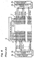
- Fig. 6 shows a conventional AC plasma display panel and its driving circuit.
- the AC plasma display panel herein after referred to as "panel” for clarity, has 2M rows of scan electrodes SCN(1)- SCN(2M) and sustain electrodes SUS(1)-SUS(2M), and N columns of data electrodes D(1)-D(N) each extending perpendicular to scan and sustain electrodes, forming a 2M by N matrix.
- Each of scan electrodes SCN(i) pairs with a corresponding sustain electrode SUS(i) so that the paired scan and sustain electrodes cooperate with one of the crossing data electrodes D(j) (integer j:1-N) to form a cell where an electric discharge will occur.
- lead wires of the paired scan and sustain electrodes SCN(i) and SUS(i) are extended out in opposite directions.
- the lead wires of the neighboring scan electrodes for example, SCN(1) and SCN(2), are extended out in opposite directions.
- the lead wires of the neighboring sustain electrodes for example, SUS(1) and SUS(2), are extended out in opposite directions. That is, in this arrangement, the odd number of scan electrodes SCN(1), SCN(3), ...,SCN(2M-1) are led out to the left side of the panel and then electrically connected with a scan electrode drive circuit 2a for driving scan electrodes with odd number.
- the even number of scan electrodes SCN(2), SCN(4), ...,SCN(2M) are led out to the right side of the panel and then electrically connected with a scan electrode drive circuit 2b for driving scan electrodes with even number.
- the even number of sustain electrodes SUS(2), SUS(4), ...,SUS(2M) are led out to the left side of the panel and then electrically connected with a sustain electrode drive circuit 3b for driving sustain electrodes with even number.
- the odd number of sustain electrodes SUS(1), SUS(3), ...,SUS(2M-1) are led out to the right side of the panel and then electrically connected with a sustain electrode drive circuit 3a for driving sustain electrodes with odd number.
- lead wires of the data electrodes D(1)-D(N) are extended out upwardly and then electrically connected with a data electrode drive circuit 4 for driving the data electrodes.
- sustain drive circuit 3a or 3b applies no signal or voltage to sustain electrodes SUS(1)-SUS(2M).
- For scanning in the first row scan electrode SCN(1) among data electrodes D(1)-D(N), selected one or more data electrodes D(j) corresponding to discharge cells for displaying are applied with a certain positive write pulse of +Vw volts from the data electrode drive circuit 4, and the first scan electrode SCN(1) is applied with a certain negative scan pulse of -Vs volts from scan electrode drive circuit 2a. This causes an electric discharge (writing discharge) at each of the intersections of the selected data electrodes D(j) and scan electrode SCN(1).
- selected one or more data electrodes D(j) corresponding to discharge cells for displaying are applied with the write pulse of +Vw volts from the data electrode drive circuit 4, and the second scan electrode SCN(2) is applied with scan pulse of -Vs volts from another scan electrode drive circuit 2b.
- This causes the electric discharge (writing discharge) at each of the intersections of the selected data electrodes D(j) and scan electrode SCN(2).
- Similar operations are performed successively for scan electrodes SCN(3) to SCN(2M), causing electric discharges at discharge cells at intersections of data electrodes D(j) and scan electrodes SCN(3) to SCN(2M).
- sustain electrode drive circuits 3a and 3b apply a negative sustain pulse of -Vm volts to every sustain electrodes SUS(1)-SUS(2M).
- This causes an initial sustain discharge between scan and sustain electrodes, SCN(i) and SUS(i), in each of the discharge cells where the writing discharge has occurred in the write period.
- a sustain discharge current flows from scan electrode drive circuit 2a through odd scan electrodes SCN(2K-1) (integer K: l to M) and then odd sustain electrodes SUS(2K-1) toward sustain electrode drive circuit 3a.
- a sustain-discharge current flows from scan electrode drive circuit 2b through even scan electrodes SCN(2K) and then even sustain electrodes SUS(2K) toward sustain electrode drive circuit 3b.
- sustain electrode drive circuits 3a and 3b apply no voltage to every sustain electrodes SUS(1)-SUS(2M), but scan electrode drive circuits 2a and 2b apply negative sustain pulse of -Vm volts.
- This causes a sustain discharge between scan and sustain electrodes, SCN(i) and SCN(i), in each of the discharge cells where the writing discharge has occurred.
- sustain discharge current flows from sustain electrode drive circuit 3a through the odd sustain electrodes SUS(2K-1) and then odd scan electrodes SCN(2K-1) toward scan electrode drive circuit 2a.
- sustain discharge current flows from sustain electrode drive circuit 3b through even sustain electrodes SUS(2K) and then scan electrodes SCN(2K) toward scan electrode drive circuit 2b.
- scan electrodes SCN(1)-SCN(2M) and sustain electrodes SUS(1)-SUS(2M) are applied with the negative sustain pulse of -Vm volts alternatively from scan electrode drive circuits 2a and 2b and sustain electrode drive circuits 3a and 3b.
- This retains sustain discharge between scan and sustain electrodes, SCN(i) and SUS(i), at each of the discharge cells where the writing discharge have occurred.
- This allows sustain discharge current to flow from sustain electrode drive circuit 3a to scan electrode drive circuit 2a and from sustain electrode drive circuit 3b to scan electrode drive circuit 2b.
- sustain discharge current flows from scan electrode drive circuit 2a to sustain electrode drive circuit 3a and from scan electrode drive circuit 2b to sustain electrode drive circuit 3b.
- all sustain electrodes SUS(1)-SUS(2M) are applied with a short negative erase pulse of -Ve volts from sustain electrode drive circuits 3a and 3b, causing an erase discharge at each of the discharge cells to erase sustain discharge.
- one frame of image is displayed on the panel by the use of light emitted during sustain discharge.
- FIG. 8 there is illustrated a schematic enlarged plan view of a part of the panel shown in Fig. 6, in particular electrodes positioned in rows from (2K-1) to (2K).
- sustain discharge current flowing at the first sustain discharge in sustain period is shown.
- bold arrows indicate the directions along which sustain discharge current flows in respective electrodes
- normal arrows indicate the directions along which sustain discharge current flows from one electrode to another.
- SCN(2K-1) and SUS(2K-1) is opposite to that sustain discharge current in the even scan and sustain electrodes, SCN(2K) and SUS(2K).
- the conventional panel is designed so that scan electrode drive circuits 2a and 2b and also sustain electrode drive circuits 3a and 3b are provided on opposite sides for odd and even electrodes. Therefore, it has been found that even a slight time shift between operations of scan electrode drive circuits 2a and 2b or between sustain electrode drive circuits 3a and 3b renders the counteraction of the electromagnetic noises unstable.
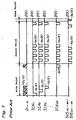
- Figs. 9(a) to 9(e) showing waveforms of sustain pulse voltage of -Vm volts and waveforms of sustain discharge current that flows through scan and sustain electrodes, at the first sustain discharge in sustain period. It should be noted that in each of Figs. 9(a) to 9(e) a horizontal axis, i.e., time axis, has different scales at its left and right portions.
- Fig. 9(a) illustrates the waveform of voltage applied to the odd scan electrodes SCN(2K-1) relative to sustain electrode drive circuit 3a when sustain pulse voltage of -Vm volts is applied from sustain electrode drive circuit 3a to the odd sustain electrode SUS(2K-1).
- Fig. 9(b) illustrates the waveform of sustain discharge current flowing from scan electrode drive circuit 2a through the odd scan electrodes SCN(2K-1) and also odd sustain electrode SUS(2K-1) to sustain electrode drive circuit 3a when sustain pulse of -Vm volts is applied from sustain electrode drive circuit 3a to the odd sustain electrode SUS(2K-1).
- Fig. 9(c) illustrates the waveform of voltage applied to the even sustain electrodes SUS(2K) relative to scan electrode drive circuit 2b when sustain pulse of -Vm volts is applied from sustain electrode drive circuit 3b to the even sustain electrodes SUS(2K).
- Fig. 9(d) illustrates the waveform of sustain discharge current flowing from sustain electrode drive circuit 3b through the even sustain electrode SUS(2K) and also even scan electrode SCN(2K) to scan electrode drive circuit 2b when sustain pulse of -Vm volts is applied from sustain electrode drive circuit 3b to the even sustain electrode SUS(2K).
- Fig. 9(e) illustrates a resultant current waveform of current waveforms shown in Figs. 9(b) and 9(d).
- the discharge sustain current is a resultant of two currents, Id and Ic.
- the current Id which serves to the actual light emission, starts flowing slightly after the application of sustain pulse voltage.
- the current IC which flows in response to a capacitance between scan and sustain electrodes, has an extremely narrow period, or is in the form of sharp peak. Therefore, the current IC is ineffective for the light emission, but causes unwanted electromagnetic noises.
- the ineffective current waveform IC is a sharp, narrow peak with a period of several nanoseconds. Then, in order to minimize the resultant current waveform as shown by solid lines in Fig. 9(e), a time shift between operations of sustain electrode drive circuits 3a and 3b should be minimized. For those purposes, responses of the circuits as well as response stability thereof should be reduced to about several hundred picoseconds, which is considered to be impossible. In view of above, the counteraction of the electromagnetic noises is not ensured positively, which is a great problem to be solved.
- an AC plasma display system includes a display panel and its driving units in which an image is displayed by sustaining discharge between neighboring scan and sustain electrodes.
- the panel 1a includes M rows of scan electrodes SCN(1)-SCN(M), and M rows of sustain electrodes SUS(1)-SUS(M) each extending parallel to scan electrodes, and N columns of data electrodes D(1)-D(N).
- Each row consists of paired scan and sustain electrodes, and scan and sustain electrodes are positioned alternately.
- Scan and sustain electrodes are led out in the opposite directions and then connected with scan electrode drive circuit 2 and sustain electrode drive circuit 3, respectively.
- Two scan electrodes defining SCN(1) are led out on the left side of the panel where they are electrically connected with scan electrode drive circuit 2
- two sustain electrodes defining SUS(1) are led out on the right side of the panel where they are electrically connected with sustain electrode drive circuit 3.
- discharge cells Intersections between paired scan and sustain electrodes and data electrodes define discharge cells, indicated at C(11)-C(MN). Therefore, in this panel, discharge cells each include two scan and sustain electrodes, forming M by N matrix.
- Fig. 23 showing an operational time chart, operations of the panel will be described.
- all of sustain electrodes SUS(1)-SUS(M) is retained at zero volt by sustain electrode drive circuit 3.
- one or more data electrodes D(j) (integer j: 1-N)for displaying image are applied with positive write pulse of +Vw volts from the data electrode drive circuit 4, and the first row scan electrode SCN(1) is applied with negative scan pulse of -Vs volts.
- This causes a write discharge at the discharge cell C(1,j), intersection of the data electrode D(j) and scan electrode SCN(1).
- sustain electrodes SUS(1)-SUS(M) are applied from sustain electrode drive circuit 3 with the negative sustain pulse of -Vm volts.
- This causes the initial sustain discharge between scan electrode SCN(i) (integer i:1-M)and sustain electrode SUS(i) at the discharge cell C(i,j) where the write discharge has been occurred.
- This causes a certain current to flow from scan electrode drive circuit 2 through scan electrode SCN(i) and then sustain electrode SUS(i) toward sustain electrode drive circuit 3.
- scan electrodes SCN(1)-SCN(M) and sustain electrodes SUS(1)-SUS(M) are applied with negative sustain pulse of -Vm volts alternately from scan electrode drive circuit 2 and sustain electrode drive circuit 3.
- one frame of image is displayed on the panel. Also, in each of discharge cell two discharges are generated, each discharge is generated between paired scan and sustain electrodes. This causes that an extended light emission is provided at each discharge cell, increasing the brightness of the resultant image.
- the conventional AC plasma display panel has a drawback that intense electromagnetic noises are generated by sustain discharge current at sustain discharging.
- Fig. 24 there is shown a part of the panel in which electrodes of from (i-1)th to (i+1)th rows are electrically connected with scan electrode drive circuit 2 and sustain electrode drive circuit 3. Also, Fig. 24 shows sustain discharge current (shown by solid lines) generated by an application of negative sustain pulse of -Vm volts to sustain electrodes SUS(1)-SUS(M) at a certain time (t) in sustain period shown in Fig. 23. As can be seen from the drawing, in each row two sustain discharge currents flowing in the paired scan and sustain electrodes run in the same direction.
- the first discharge current from one scan electrode SCN(i,a) to one sustain electrode SUS(i,a) flows in the same direction as the second discharge current from the other scan electrode SCN(i,b) to the other sustain electrode SUS(i,b).
- the two sustain discharge currents flows in the same direction from scan to sustain electrodes, causing electromagnetic noises with the same phase due to sustain discharge currents.
- the electromagnetic noises with the same phase are superimposed to generate a greater electromagnetic noise which would be emitted from the panel. Also, as indicated by dotted lines in Fig.
- the current flows through the capacitance between both paired scan and sustain electrodes, e.g., from scan electrode SCN(i,b) to sustain electrode SUS(i,a) in the same direction, i.e., left to right.
- the current flows through the capacitance between both paired scan and sustain electrodes, e.g., from scan electrode SCN(i,a) to sustain electrode SUS(i-1,b) in the same direction, i.e., left to right. Therefore, the electromagnetic noise generated by the current flowing through capacitance has the same phase as that generated by sustain discharge current in every row.
- an object of the present invention is to provide an AC plasma display panel capable of minimizing the electromagnetic noise possibly caused by the current flowing in the electrodes.
- an AC plasma display panel of the present invention includes a plurality of parallel scan electrodes; a plurality of parallel sustain electrodes, each of the sustain electrodes extending parallel to the plurality of scan electrodes, wherein the plurality of scan and sustain electrodes are positioned so that each one of the scan and sustain electrodes positions adjacent to and paired with the other one of scan and sustain electrodes; a plurality of parallel data electrodes, the data electrodes extending substantially perpendicular to the scan and sustain electrodes; means for applying a certain current to the scan and sustain electrodes so that the current in the paired scan and sustain electrodes respectively flows in opposite directions each other.
- Another AC plasma display panel of the present invention includes a plurality of discharge cells, the plurality of discharge cells being arrange in a matrix made of plurality of rows and columns, wherein each of the discharge cells includes two pairs of scan and sustain electrodes extending in one direction and a data electrode extending substantially perpendicular to the one direction, means for applying a certain current to the scan and sustain electrodes so that the current in one of the two pairs flows in one direction and the current in the other of the two pairs flows in the opposite direction.
- Another AC plasma display panel of the present invention includes a plurality of parallel scan electrodes; a plurality of parallel sustain electrodes, each of the sustain electrodes extending parallel to the plurality of scan electrodes, wherein the plurality of scan and sustain electrodes are positioned so that each one of the scan and sustain electrodes positions adjacent to and paired with the other one of scan and sustain electrodes; a plurality of parallel data electrodes, the data electrodes extending substantially perpendicular to the scan and sustain electrodes to form discharge cells at intersections of the scan and sustain electrodes and the data electrodes, wherein each of the discharge cells is defined by two pairs of scan and sustain electrodes and the data electrode; means for applying a certain current to each of the paired scan and sustain electrodes, the current in one of the two pairs flows in one direction and the current in the other of the two pairs flows in the opposite direction.
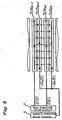
- Fig. 1 shows an AC plasma display panel according to the first embodiment of the present invention.
- the panel 5 includes 2M scan electrodes, SCN(1)-SCN(2M), and 2M sustain electrodes, SUS(1)-SUS(2M), extending in the same direction. Also, scan electrodes SCN(1)-SCN(2M) pair with sustain electrodes SUS(1)-SUS(2M), respectively.
- the panel 5 further includes N data electrodes, D(1)-D(n) extending perpendicular to scan and sustain electrodes, forming a matrix of 2M by N therewith.
- the paired scan and sustain electrodes, SCN(i) and SUS(i) are led out to the same side.
- the paired scan and sustain electrodes, SCN(1) and SUS(1) are led out to the left side of the panel 5.
- the neighboring pairs are led out on the opposite sides of the panel 5.
- the paired electrodes SCN(1) and SUS(1) are led out to the left side and another paired electrodes SCN(2) and SUS(2) are led out to the right side of the panel 5.
- the lead wires of the odd scan electrodes SCN(2K-1) and sustain electrodes SUS(2K-1) are extended out to the left side of the panel 5.
- the lead wires of the even scan electrodes SCN(2K) and sustain electrodes SUS(2K) are extended out to the right side of the panel 5.
- the odd scan electrodes SCN(2K-1) are electrically connected with a scan electrode drive circuit 2a for applying a certain pulse or voltage to drive the odd scan electrodes.
- the odd sustain electrodes SUS(2K-1) are electrically connected with a sustain electrode drive circuit 3a for applying a certain pulse or voltage to drive the odd sustain electrodes.
- the even scan electrodes SCN(2K) are electrically connected with a scan electrode drive circuit 2b for applying a certain pulse or voltage to drive the even scan electrodes.
- the even sustain electrodes SUS(2K) are electrically connected with a sustain electrode drive circuit 3b for applying a certain pulse or voltage to drive the even sustain electrodes.
- the data electrodes D(1)-D(N) are led out upwardly and electrically connected with a data electrode drive circuit 4 for applying a certain pulse or voltage to drive the data electrodes.
- the panel 5 can be operated in the conventional manner shown according to the operational time chart shown in Fig. 7 which has been described above and therefore no further description will be made to this.
- Fig. 2 shows an arrangement including paired electrodes of (2K-1)-th and (2K)-th rows in the panel 5 shown in Fig. 1.
- This drawing illustrates directions of sustain discharge currents flowing at the first sustain discharge in sustain period, in which each of bold arrows shows sustain discharge current flowing in the electrode and each of normal arrows shows sustain discharge current flowing between neighboring electrodes.
- sustain discharge currents in the paired odd scan electrode SCN(2K-1) and sustain electrode SUS(2K-1) are directed in the opposite directions.
- sustain discharge currents in the paired even scan electrode SCN(2K) and sustain electrode SUS(2K) are directed in the opposite directions.
- the paired scan and sustain electrodes are provided with a certain current simultaneously so that the current flows in the paired scan and sustain electrodes in the opposite directions because they are applied from any one of scan and sustain electrode drive circuits, 2a, 2b, 3a, and 3b.
- electromagnetic waves generated by sustain discharge currents flowing in the paired scan and sustain electrodes, SCN(2K-1) and SUS(2K-1), can be designed so that they have vector components with the sane magnitude in the opposite directions.
- electromagnetic waves generated by sustain discharge currents flowing in the paired scan and sustain electrodes, SCN(2K) and SUS(2K) can be designed so that they have vector components with the same magnitude in the opposite directions. This allows the generated electromagnetic noises to counteract or cancel to each other.
- Figs. 3(a) to 3(d) show waveforms of sustain pulse of -Vm volts and current flowing in scan and sustain electrodes.
- a horizontal axis i.e., time axis, has different scales at its left and right portions.
- Fig. 3(a) illustrates the waveform of voltage applied to the odd scan electrodes SCN(2K-1) when sustain pulse of -Vm volts is applied from sustain electrode drive circuit 3a to the odd sustain electrode SUS(2K-1), and also illustrates the waveform of voltage applied to the even sustain electrodes SUS(2K) when sustain pulse of -Vm volts is applied from sustain electrode drive circuit 3b to the even sustain electrode SUS(2K).
- Fig. 3(b) illustrates the waveform of sustain discharge current flowing from scan electrode drive circuit 2a to the odd scan electrodes SCN(2K-1) or from scan electrode drive circuit 2b to the even scan electrode SCN(2K) when sustain pulse voltage of -Vm volts is applied from sustain electrode drive circuit 3a to the odd sustain electrode SUS(2K-1).
- Fig. 3(c) illustrates the waveform of sustain discharge current flowing from sustain electrode SUS(2K-1) to sustain electrode drive circuit 3a, or from sustain electrode SUS(2K) to sustain electrode drive circuit 3b.
- Fig. 3(d) illustrates a resultant current waveform of current waveforms shown in Figs. 3(b) and 3(c).
- both of the waveforms shown in Figs. 3(b) and 3(c) are waveforms of sustain discharge current supplied from sustain drive circuit 3a or 3b and, therefore, no time shift exists between waveforms of sustain discharge currents shown in Figs. 3(b) and 3(c) irrelevant to the operations of sustain electrode drive circuits 3a and 3b.
- the lead wires of the paired scan and sustain electrodes are extended out to the opposite directions, left and right sides, alternately. Then, the extended lead wires occupy a reduced area. This in turn means that a greater gap can be provided between neighboring lead wires of the panel.
- the current flowing in sustain electrode SUS(2K-1) and scan electrode SCN(2K) is oriented opposite to that in sustain electrode SUS(2K) and scan electrode SCN(2K+1). Therefore, a possible time shift in the operations of between sustain electrode drive Circuits 3a and 3b or scan electrode drive circuits 2a and 2b results in that the electromagnetic noises may not be cancelled by another.
- the paired scan and sustain electrodes are led out in the same direction and the pairs are directed in opposite directions alternately, similar and other advantages can be obtained provided that the paired electrodes are led out to the same direction.
- Fig. 4 shows another AC plasma display panel 6 according to the second embodiment of the present invention.
- the panel is similar to that described in the first embodiment except that all scan electrodes SCN(1)-SCN(2M) are led out to the left side of the panel 6 and then electrically connected with scan electrode drive circuit 2 for driving those electrodes, and also all sustain electrodes SUS(1)-SUS(2M) are led out to the left side of the panel 6 and then electrically connected with sustain electrode drive circuit 3 for driving those electrodes. Further, the data electrodes D(1)-D(N) are led out upwardly and then electrically connected with the data drive circuit 4 for driving those electrodes.
- each of scan electrode drive circuit 2 and sustain electrode drive circuit 3 is made of one circuit and not separated into two as shown in the previous embodiment, the panel 6 can be operated in the conventional manner according to the operational time chart shown in Fig. 7 which has been described above and therefore no further description will be made to this.
- Fig. 5 shows an arrangement including paired electrodes of (2K-1)-th and (2K)-th rows in the panel 6 shown in Fig. 4.
- the paired scan electrode SCN(i) and sustain electrode SUS(i) are applied with sustain discharge current in opposite directions.
- a sustain discharge current always flows simultaneously in the scan and sustain electrodes in the opposite directions because it is applied from scan electrode drive circuit 2 or sustain electrode drive circuit 3.
- This causes the electromagnetic noises emitted from sustain discharge currents flowing through the paired scan and sustain electrodes, SCN(i) and SUS(i), respectively to be cancelled by another.
- the same descriptions made to the first embodiment for the noise cancellation, using voltage and current waveforms can be applied equally to this embodiment and, therefore, no further description will be made to this.
- the current flows in opposite directions in the paired scan and sustain electrodes, minimizing the electromagnetic noises generated by the current.
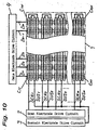
- FIG. 10 there is shown another AC plasma display system having a panel 7 and its drive circuit.
- One of the paired scan electrodes and one of the paired sustain electrodes are electrically connected with scan electrode drive circuit 2 and sustain electrode drive circuit 3, respectively, positioned on the opposite side of the panel.
- each row the plurality of electrodes, i.e., first scan electrode connected with scan electrode drive circuit 2, first sustain electrode, second sustain electrode connected with sustain electrode drive circuit 3, and the second scan electrode, are positioned in this order.
- each of M rows of scan electrodes SCN(1)-SCN(M) includes two scan electrodes connected to each other.
- each of M rows of sustain electrodes SUS(1)-SUS(M) includes two sustain electrodes connected to each other.
- M rows of scan electrodes SCN(1)-SCN(M) and sustain electrodes SUS(1)-SUS(M) define discharge cells C(1,1)-C(M,N) at intersections with data electrodes D(1)-D(N). In this manner, the panel 7 is formed with a number of discharge cells in the form of M by N matrix. Also, each discharge cell is defined by two pairs of scan and sustain electrodes.
- the panel 7 can be operated in the conventional manner shown according to the operational time chart shown in Fig. 23 which has been described above and therefore no further description will be made to this.
- Fig. 11 shows electrodes in (i-1)-th to (i+1)-th rows together with scan and sustain electrode drive circuits 2 and 3 connected to the electrodes. Also, Fig. 11 shows sustain discharge current (shown by solid lines) generated by an application of negative sustain pulse of - Vm volts to all of sustain electrode SUS(1)-SUS(M) at a certain time (t) in sustain period shown in Fig. 23. As can be seen from the drawing, in each row two sustain discharge currents flowing in the paired scan and sustain electrodes run in the opposite directions.
- the first discharge current from one scan electrode SCN(i,a) to one sustain electrode SUS(i,a) flows in the opposite direction against the second discharge current from the other scan electrode SCN(i,b) to the other sustain electrode SUS(i,b).
- discharge sustain current from scan electrode SCN(i,a) to sustain electrode SUS(i,a) flows from sustain electrode SUS(i,b) to sustain electrode drive circuit 3 as shown by long and short dotted line.
- Another discharge sustain current from scan electrode SCN(i,b) to sustain electrode SUS(i,b) flows from scan electrode drive circuit 2 to scan electrode SCN(i,a) as shown by another long and short dotted line.
- directions indicated by respective long and short dotted lines are opposite to the other.
- Fig. 12 shows an AC plasma display panel according to the fourth embodiment of the present invention.
- the AC plasma display panel includes a panel 8 and its drive circuit, in which a sustain discharge is generated between each pair of scan and sustain electrodes for display.
- each row has two pairs of scan and sustain electrodes.
- the two scan electrodes as well as the two sustain electrodes are connected to each other on one side of the panel, and one of the two scan electrodes and one of the two sustain electrodes are electrically connected with scan electrode drive circuit 2 and sustain electrode drive circuit 3, respectively.
- the panel includes M rows of scan electrodes SCN(1)-SCN(M), each of which row including two scan electrodes connected to each other.
- the panel includes M rows of sustain electrodes SUS(1)-SUS(M), each of which row including two sustain electrodes connected to each other.
- M rows of scan and sustain electrodes SCN(1)-SCN(M) and SUS(1)-SUS(M), cooperate with N columns of data electrodes D(1)-D(N) to form a plurality of discharge cells C(1,1)-C(M,N) at their intersections.
- the panel 8 includes two pairs of scan and sustain electrodes in each discharge cell and defines discharge cells C(1,1)-C(M,N) in the form of M by N matrix.
- the panel 8 can be operated in the conventional manner shown according to the operational time chart shown in Fig. 23 which has been described above and therefore no further description will be made to this.
- Fig. 13 shows electrodes in (i-1)-th to (i+1)-th rows together with scan and sustain electrode drive circuits 2 and 3 connected to the electrodes. Also, Fig. 13 shows sustain discharge current (shown by solid lines) generated by an application of negative sustain pulse of - Vm volts to all of sustain electrode SUS(1)-SUS(M) at a certain time (t) in sustain period shown in Fig. 23. As can be seen from the drawing, in each row two sustain discharge currents flowing in the paired scan and sustain electrodes run in the opposite directions.
- the first discharge current from one scan electrode SCN(i,a) to one sustain electrode SUS(i,a) flows in the opposite direction against the second discharge current from the other scan electrode SCN(i,b) to the other sustain electrode SUS(i,b).
- sustain discharge current from scan electrode SCN(i,a) to sustain electrode SUS(i,a) flows from scan electrode drive circuit 2 to scan electrode SCN(i,b) as shown by long and short dotted line.
- Another sustain discharge current from scan electrode SCN(i,b) to sustain electrode SUS(i,b) flows from sustain electrode SUS(i,a) to sustain electrode drive circuit 3 as shown by another long and short dotted line.
- directions indicated by respective long and short dotted lines are opposite to the other.
- electromagnetic noises generated by two discharge currents that flow the paired scan and sustain electrodes take opposite phases, which functions to cancel the other to minimize the electromagnetic noise from the panel.
- electromagnetic noise generated in one row is cancelled by electromagnetic noise generated in the neighboring row, minimizing the electromagnetic noise emitted from the panel.
- a small portion of the electromagnetic noise generated from the panel is from others rather than sustain pulses, which is not problematic to the practical use of the panel.
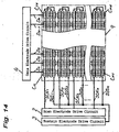
- Fig. 14 shows an AC plasma display panel according to the fifth embodiment of the present invention.
- the AC plasma display panel includes a panel 9 and its drive circuit, in which a sustain discharge is generated between each pair of scan and sustain electrodes for display.
- each row has two pairs of scan and sustain electrodes.
- the two scan electrodes as well as the two sustain electrodes are connected to each other on one side of the panel, and one of the two scan electrodes and one of the two sustain electrodes are electrically connected with scan electrode drive circuit 2 and sustain electrode drive circuit 3, respectively.
- the panel includes M rows of scan electrodes SCN(1)-SCN(M), each of which row including two scan electrodes connected to each other.
- the panel includes M rows of sustain electrodes SUS(1)-SUS(M), each of which row including two sustain electrodes connected to each other.
- M rows of scan and sustain electrodes SCN(1)-SCN(M) and SUS(1)-SUS(M), cooperate with N columns of data electrodes D(1)-D(N) to form a plurality of discharge cells C(1,1)-C(M,N) at their intersections.
- the panel 9 includes two pairs of scan and sustain electrodes in each discharge cell and defines discharge cells C(1,1)-C(M,N) in the form of M by N matrix.
- the panel 9 can be operated in the conventional manner shown according to the operational time chart shown in Fig. 23 which has been described above and therefore no further description will be made to this.
- Fig. 15 shows electrodes in (i-1)-th to (i+1)-th rows together with scan and sustain electrode drive circuits 2 and 3 connected to the electrodes. Also, Fig. 15 shows sustain current (shown by solid lines) generated by an application of negative sustain pulse of -Vm volts to all of sustain electrode SUS(1)-SUS(M) at a certain time (t) in sustain period shown in Fig. 23. As can be seen from the drawing, in each row two sustain discharge currents flowing in the paired scan and sustain electrodes run in the opposite directions.
- the first discharge current from one scan electrode SCN(i,a) to one sustain electrode SUS(i,a) flows in the opposite direction against the second discharge current from the other scan electrode SCN(i,b) to the other sustain electrode SUS(i,b).
- sustain discharge current from scan electrode SCN(i,a) to sustain electrode SUS(i,a) flows from sustain electrode SUS(i,b) to sustain electrode drive circuit 3 as shown by long and short dotted line.
- Another discharge sustain current from scan electrode SCN(i,b) to sustain electrode SUS(i,b) flows from scan electrode drive circuit 2 to scan electrode SCN(i,a) as shown by another long and short dotted line.
- directions indicated by respective long and short dotted lines are opposite to the other.
- electromagnetic noises generated by two discharge currents that flow the paired scan and sustain electrodes take opposite phases, which function to cancel the other to minimize the electromagnetic noise from the panel.
- each row current flows through the capacitance between a pair of scan and sustain electrodes and another pair of scan and sustain electrodes in the same row, e.g., from scan electrode SCN(i,b) to sustain electrode SUS(i,a).
- the current in scan electrode SCN(i,b) and that in sustain electrode SUS(i,a) flow in opposite directions.
- current flows through the capacitance between a pair of scan and sustain electrodes and a pair of scan and sustain electrodes in the neighboring row e.g., from scan electrode SCN(i,a) to sustain electrode SUS(i-1,b).
- Fig. 16 shows an AC plasma display panel according to the sixth embodiment of the present invention.
- the AC plasma display panel includes a panel 10 and its drive circuit, in which a sustain discharge is generated between each pair of scan and sustain electrodes for display.
- each row has two pairs of scan and sustain electrodes.
- the two scan electrodes as well as the two sustain electrodes are connected to each other on one side of the panel, and one of the two scan electrodes and one of the two sustain electrodes are electrically connected with scan electrode drive circuit 2 and sustain electrode drive circuit 3, respectively.
- the panel includes M rows of scan electrodes SCN(1)-SCN(M), each of which row including two scan electrodes connected to each other.
- the panel includes M rows of sustain electrodes SUS(1)-SUS(M), each of which row including two sustain electrodes connected to each other.
- M rows of scan and sustain electrodes SCN(1)-SCN(M) and SUS(1)-SUS(M), cooperate with N columns of data electrodes D(1)-D(N) to form a plurality of discharge cells C(1,1)-C(M,N) at their intersections.
- the panel 10 includes two pairs of scan and sustain electrodes in each discharge cell and defines discharge cells C(1,1)-C(M,N) in the form of M by N matrix.
- the panel 10 can be operated in the conventional manner shown according to the operational time chart shown in Fig. 23 which has been described above and therefore no further description will be made to this.
- Fig. 17 shows electrodes in (i-1)-th to (i+1)-th rows together with scan and sustain electrode drive circuits 2 and 3 connected to the electrodes. Also, Fig. 17 shows sustain discharge current (shown by solid lines) generated by an application of negative sustain pulse of - Vm volts to all of sustain electrode SUS(1)-SUS(M) at a certain time (t) in sustain period shown in Fig. 23. As can be seen from the drawing, in each row two sustain discharge currents flowing in the paired scan and sustain electrodes run in the opposite directions.
- the first discharge current from one scan electrode SCN(i,a) to one sustain electrode SUS(i,a) flows in the opposite direction against the second discharge current from the other scan electrode SCN(i,b) to the other sustain electrode SUS(i,b).
- sustain discharge current from scan electrode SCN(i,a) to sustain electrode SUS(i,a) flows from scan electrode drive circuit 2 to scan electrode SCN(i,b) as shown by long and short dotted line.
- Another discharge sustain current from scan electrode SCN(i,b) to sustain electrode SUS(i,b) flows from sustain electrode SUS(i,a) to sustain electrode drive circuit 3 as shown by another long and short dotted line.
- directions indicated by respective long and shrt dotted lines are opposite to the other.
- electromagnetic noises generated by two discharge currents that flow the paired scan and sustain electrodes take opposite phases, which function to cancel the other to minimize the electromagnetic noise from the panel.
- current from scan or sustain electrode in one pair to scan or sustain electrode in the other pair flows in opposite directions in those electrodes.
- current flows in one direction in scan electrode SCN(i,a) and current flows in the opposite direction in sustain electrode SUS(i,b).
- no current flows from one row to the neighboring row e.g., from sustain electrode SUS(i-1,b) to sustain electrode SUS(i,a), because they are on the same voltage level. Therefore, electromagnetic noise from the AC Plasma display panel can be reduced significantly. Note that a small portion of the electromagnetic noise generated from the panel is from others rather than sustain pulses, which is not problematic to the practical use of the panel.
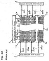
- Fig. 18 shows an AC plasma display panel according to the seventh embodiment of the present invention.
- the AC plasma display panel includes a panel 11 and its drive circuit, in which a sustain discharge is generated between each pair of scan and sustain electrodes for display.
- each row has two pairs of scan and sustain electrodes.
- the two scan electrodes as well as the two sustain electrodes are connected to each other on one side of the panel, and one of the two scan electrodes and one of the two sustain electrodes are electrically connected with scan electrode drive circuit 2 and sustain electrode drive circuit 3, respectively.
- the panel includes M rows of scan electrodes SCN(1)-SCN(M), each of which row including two scan electrodes connected to each other.
- the panel includes M rows of sustain electrodes SUS(1)-SUS(M), each of which row including two sustain electrodes connected to each other.
- M rows of scan and sustain electrodes SCN(1)-SCN(M) and SUS(1)-SUS(M), cooperate with N columns of data electrodes D(1)-D(N) to form a plurality of discharge cells C(1,1)-C(M,N) at their intersections.
- the panel 11 includes two pairs of scan and sustain electrodes in each discharge cell and defines discharge cells C(1,1)-C(M,N) in the form of M by N matrix.
- the panel 11 can be operated in the conventional manner shown according to the operational time chart shown in Fig. 23 which has been described above and therefore no further description will be made to this.
- Fig. 19 shows electrodes in (i-1)th to (i+1)th rows together with scan and sustain electrode drive circuits 2 and 3 connected to the electrodes. Also, Fig. 19 shows sustain discharge current (shown by solid lines) generated by an application of negative sustain pulse of - Vm volts to all of sustain electrode SUS(1)-SUS(M) at a certain time (t) in sustain period shown in Fig. 23. As can be seen from the drawing, in each sustain discharge current in every row, current in scan electrode and that in sustain electrode in the paired scan and sustain electrodes run in the opposite directions.
- discharge sustain current from scan electrode SCN(i,b) to sustain electrode SUS(i,b) flows from scan electrode drive circuit 2 via scan electrode SCN(i,a) and to sustain electrode drive circuit 3 via sustain electrode SUS(i,a), as shown by long and short dotted lines. Also, directions indicated by respective long and short dotted lines are opposite to the other.
- electromagnetic noises generated by the current in scan electrode and that in sustain electrode in the paired scan and sustain electrodes take opposite phases respectively, which function to cancel each other to minimize the electromagnetic noise from the panel.
- one current from scan or sustain electrode in one pair to scan or sustain electrode in the other pair corresponds to that flows, for example, between sustain electrode SUS(i,b) and sustain electrode SUS(i,a) having the same voltage level, can be zero.
- current flowing between neighboring rows corresponds to that flows, for example, between scan electrode SCN(i,a) and scan electrode SCN(i-1,b) having the same voltage level. Therefore, one electromagnetic noise is cancelled by another, minimizing the electromagnetic noise from the panel. Note that a small portion of the electromagnetic noise generated from the panel is from others rather than sustain pulses, which is not problematic to the practical use of the panel.
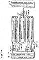
- Fig. 20 shows an AC plasma display panel according to the fourth embodiment of the present invention.
- the AC plasma display panel includes a panel 12 and its drive circuit, in which a sustain discharge is generated between each pair of scan and sustain electrodes for display.
- each row has two pairs of scan and sustain electrodes.
- the two scan electrodes as well as the two sustain electrodes are connected to each other on the right side of the panel, and one of the two scan electrodes and one of the two sustain electrodes are electrically connected with scan electrode drive circuit 2a and sustain electrode drive circuit 3a, respectively, on the left side of the panel.
- the two scan electrodes as well as the two sustain electrodes are connected to each other on the left side of the panel, and one of the two scan electrodes and one of the two sustain electrodes are electrically connected with scan electrode drive circuit 2b and sustain electrode drive circuit 3b, respectively, on the right side of the panel.
- the panel 12 can be operated in the conventional manner shown according to the operational time chart shown in Fig. 23 in which scan electrode drive circuits 2a and 2b may be driven at the same time and also sustain electrode drive circuits 3a and 3b may be driven at the same time. Those operations are the same as described above and therefore no further description will be made to this.
- Fig. 21 shows electrodes in (i-1)th to (i+1)th rows together with scan and sustain electrode drive circuits 2 and 3 connected to the electrodes. Also, Fig. 21 shows sustain discharge current (shown by solid lines) generated by an application of negative sustain pulse of - Vm volts to all of sustain electrode SUS(1)-SUS(M) at a certain time (t) in sustain period shown in Fig. 23. As can be seen from the drawing, in each row two sustain discharge currents flowing in the paired scan and sustain electrodes run in the opposite directions.
- the first discharge current from one scan electrode SCN(i,a) to one sustain electrode SUS(i,a) flows in the opposite direction against the second discharge current from the other scan electrode SCN(i,b) to the other sustain electrode SUS(i,b).
- sustain discharge current from scan electrode SCN(i,a) to sustain electrode SUS(i,a) flows via sustain electrode SUS(i,b) to sustain electrode drive circuit 3b as shown by long and short dotted line.
- Another discharge sustain current from scan electrode SCN(i,b) to sustain electrode SUS(i,b) flows from scan electrode drive circuit 2b via scan electrode SCN(i,a) as shown by another long and short dotted line.
- directions indicated by respective long and short dotted lines are opposite to the other.
- electromagnetic noises generated by two discharge currents that flow the paired scan and sustain electrodes take opposite phases, which function to cancel the other to minimize the electromagnetic noise from the panel.
- one current from scan or sustain electrode in one pair to scan or sustain electrode in the other pair corresponds to that flows, for example, between sustain electrode SUS(i,b) and sustain electrode SUS(i,a) having the same voltage level, can be zero.
- current flows between neighboring rows only when pulses from two scan electrode drive circuit 2a and 2b does not applied at the same time. Even when such current flows, current flows in scan electrode SCN(i-1,b) in opposite direction to that in scan electrode SCN(i,a), for example. Therefore, one electromagnetic noise is cancelled by another, minimizing the electromagnetic noise from the panel. Note that a small portion of the electromagnetic noise generated from the panel is from others rather than sustain pulses, which is not problematic to the practical use of the panel.
Landscapes
- Engineering & Computer Science (AREA)
- Physics & Mathematics (AREA)
- Power Engineering (AREA)
- Plasma & Fusion (AREA)
- Computer Hardware Design (AREA)
- General Physics & Mathematics (AREA)
- Theoretical Computer Science (AREA)
- Control Of Indicators Other Than Cathode Ray Tubes (AREA)
- Control Of Gas Discharge Display Tubes (AREA)
Applications Claiming Priority (4)
| Application Number | Priority Date | Filing Date | Title |
|---|---|---|---|
| JP10106599 | 1999-04-08 | ||
| JP11101065A JP2000293137A (ja) | 1999-04-08 | 1999-04-08 | Ac型プラズマ表示装置 |
| JP10227699A JP3711784B2 (ja) | 1999-04-09 | 1999-04-09 | Ac型プラズマ表示装置 |
| JP10227699 | 1999-04-09 |
Publications (2)
| Publication Number | Publication Date |
|---|---|
| EP1043706A2 true EP1043706A2 (de) | 2000-10-11 |
| EP1043706A3 EP1043706A3 (de) | 2002-10-02 |
Family
ID=26441989
Family Applications (1)
| Application Number | Title | Priority Date | Filing Date |
|---|---|---|---|
| EP00107665A Withdrawn EP1043706A3 (de) | 1999-04-08 | 2000-04-10 | Wechselstrom Pasmaanzeigegerät |
Country Status (5)
| Country | Link |
|---|---|
| US (1) | US6320326B1 (de) |
| EP (1) | EP1043706A3 (de) |
| KR (1) | KR20000071614A (de) |
| CN (1) | CN1283864A (de) |
| TW (1) | TW451172B (de) |
Cited By (3)
| Publication number | Priority date | Publication date | Assignee | Title |
|---|---|---|---|---|
| WO2005117486A1 (ja) | 2004-05-31 | 2005-12-08 | Matsushita Electric Industrial Co., Ltd. | プラズマディスプレイ装置 |
| EP1221685A3 (de) * | 2000-12-22 | 2008-02-20 | Hitachi, Ltd. | Plasma-Anzeigegerät mit reduzierten Spannungseinbrüchen entlang leitender Linien |
| CN100458885C (zh) * | 2003-10-08 | 2009-02-04 | 三星Sdi株式会社 | 用于维持周期的显示板驱动方法和使用该方法的显示板 |
Families Citing this family (15)
| Publication number | Priority date | Publication date | Assignee | Title |
|---|---|---|---|---|
| JP3630584B2 (ja) * | 1999-04-28 | 2005-03-16 | パイオニア株式会社 | ディスプレイパネルの駆動方法 |
| TW473761B (en) * | 1999-10-27 | 2002-01-21 | Matsushita Electric Industrial Co Ltd | AC plasma display panel |
| EP1399910A2 (de) * | 2000-09-18 | 2004-03-24 | Koninklijke Philips Electronics N.V. | Plasmaanzeigetafel mit erhaltungselektroden |
| JP3485874B2 (ja) * | 2000-10-04 | 2004-01-13 | 富士通日立プラズマディスプレイ株式会社 | Pdpの駆動方法および表示装置 |
| JP3688206B2 (ja) * | 2001-02-07 | 2005-08-24 | 富士通日立プラズマディスプレイ株式会社 | プラズマディスプレイパネルの駆動方法および表示装置 |
| JP2003045338A (ja) * | 2001-07-30 | 2003-02-14 | Nec Corp | プラズマディスプレイ装置 |
| KR100467431B1 (ko) * | 2002-07-23 | 2005-01-24 | 삼성에스디아이 주식회사 | 플라즈마 디스플레이 패널 및 그 구동 방법 |
| JP2004184682A (ja) * | 2002-12-03 | 2004-07-02 | Fujitsu Hitachi Plasma Display Ltd | プラズマディスプレイ装置 |
| KR100578887B1 (ko) * | 2004-05-31 | 2006-05-11 | 삼성에스디아이 주식회사 | 플라즈마 디스플레이 패널 및 그 구동방법 |
| KR20050119775A (ko) * | 2004-06-17 | 2005-12-22 | 삼성에스디아이 주식회사 | 플라즈마 디스플레이 패널 및 그 구동회로장치 |
| KR20060058361A (ko) * | 2004-11-25 | 2006-05-30 | 삼성에스디아이 주식회사 | 플라즈마 디스플레이 패널 |
| KR100719084B1 (ko) * | 2005-04-21 | 2007-05-17 | 엘지전자 주식회사 | 플라즈마 디스플레이 패널, 장치, 패널의 구동 장치 및구동 방법 |
| CN101641727A (zh) * | 2007-04-25 | 2010-02-03 | 松下电器产业株式会社 | 等离子显示装置 |
| KR20090031073A (ko) * | 2007-09-21 | 2009-03-25 | 엘지전자 주식회사 | 플라즈마 디스플레이 장치 |
| CN106714434B (zh) * | 2015-07-17 | 2024-04-09 | 核工业西南物理研究院 | 成对电极共面放电等离子体发生装置 |
Citations (1)
| Publication number | Priority date | Publication date | Assignee | Title |
|---|---|---|---|---|
| WO1997019438A1 (en) * | 1995-11-22 | 1997-05-29 | Orion Electric Co. Ltd. | Gas discharge display panel of alternating current with a reverse surface discharge |
Family Cites Families (11)
| Publication number | Priority date | Publication date | Assignee | Title |
|---|---|---|---|---|
| US4320418A (en) * | 1978-12-08 | 1982-03-16 | Pavliscak Thomas J | Large area display |
| KR940007502B1 (ko) * | 1992-03-04 | 1994-08-18 | 삼성전관 주식회사 | 플라즈마 디스플레이 판넬의 구조 및 구동방법 |
| JP3307486B2 (ja) * | 1993-11-19 | 2002-07-24 | 富士通株式会社 | 平面表示装置及びその制御方法 |
| US5656893A (en) * | 1994-04-28 | 1997-08-12 | Matsushita Electric Industrial Co., Ltd. | Gas discharge display apparatus |
| JP2755201B2 (ja) * | 1994-09-28 | 1998-05-20 | 日本電気株式会社 | プラズマディスプレイパネルの駆動回路 |
| JP3672669B2 (ja) * | 1996-05-31 | 2005-07-20 | 富士通株式会社 | 平面表示装置の駆動装置 |
| JP2950270B2 (ja) * | 1997-01-10 | 1999-09-20 | 日本電気株式会社 | 交流放電メモリ型プラズマディスプレイパネルの駆動方法 |
| JP3897896B2 (ja) * | 1997-07-16 | 2007-03-28 | 三菱電機株式会社 | プラズマディスプレイパネルの駆動方法及びプラズマディスプレイ装置 |
| JP3019031B2 (ja) * | 1997-07-18 | 2000-03-13 | 日本電気株式会社 | プラズマディスプレイ |
| JPH1185098A (ja) * | 1997-09-01 | 1999-03-30 | Fujitsu Ltd | プラズマ表示装置 |
| US5852347A (en) * | 1997-09-29 | 1998-12-22 | Matsushita Electric Industries | Large-area color AC plasma display employing dual discharge sites at each pixel site |
-
2000
- 2000-04-07 US US09/545,865 patent/US6320326B1/en not_active Expired - Lifetime
- 2000-04-08 TW TW089106561A patent/TW451172B/zh not_active IP Right Cessation
- 2000-04-08 KR KR1020000018419A patent/KR20000071614A/ko not_active Ceased
- 2000-04-10 CN CN00105751.0A patent/CN1283864A/zh active Pending
- 2000-04-10 EP EP00107665A patent/EP1043706A3/de not_active Withdrawn
Patent Citations (1)
| Publication number | Priority date | Publication date | Assignee | Title |
|---|---|---|---|---|
| WO1997019438A1 (en) * | 1995-11-22 | 1997-05-29 | Orion Electric Co. Ltd. | Gas discharge display panel of alternating current with a reverse surface discharge |
Cited By (5)
| Publication number | Priority date | Publication date | Assignee | Title |
|---|---|---|---|---|
| EP1221685A3 (de) * | 2000-12-22 | 2008-02-20 | Hitachi, Ltd. | Plasma-Anzeigegerät mit reduzierten Spannungseinbrüchen entlang leitender Linien |
| CN100458885C (zh) * | 2003-10-08 | 2009-02-04 | 三星Sdi株式会社 | 用于维持周期的显示板驱动方法和使用该方法的显示板 |
| US7605779B2 (en) | 2003-10-08 | 2009-10-20 | Samsung Sdi Co., Ltd. | Panel driving method for sustain period and display panel using the same |
| WO2005117486A1 (ja) | 2004-05-31 | 2005-12-08 | Matsushita Electric Industrial Co., Ltd. | プラズマディスプレイ装置 |
| EP1753262A4 (de) * | 2004-05-31 | 2010-07-28 | Panasonic Corp | Plasmaanzeigeeinrichtung |
Also Published As
| Publication number | Publication date |
|---|---|
| CN1283864A (zh) | 2001-02-14 |
| US6320326B1 (en) | 2001-11-20 |
| TW451172B (en) | 2001-08-21 |
| KR20000071614A (ko) | 2000-11-25 |
| EP1043706A3 (de) | 2002-10-02 |
Similar Documents
| Publication | Publication Date | Title |
|---|---|---|
| US6320326B1 (en) | AC plasma display apparatus | |
| US6091380A (en) | Plasma display | |
| US6288692B1 (en) | Plasma display for high-contrast interlacing display and driving method therefor | |
| KR100769787B1 (ko) | 플라즈마 디스플레이 장치 | |
| EP0969446B1 (de) | Verfahren zur Ansteuerung einer Plasmaanzeigetafel | |
| KR100337882B1 (ko) | 플라즈마 표시 패널의 구동방법 | |
| KR19990087877A (ko) | 플라즈마디스플레이패널구동방법및구동장치 | |
| JP3231569B2 (ja) | プラズマディスプレイパネルの駆動方法および駆動装置 | |
| KR20020065828A (ko) | 플라스마 디스플레이 패널의 구동 방법 및 표시 장치 | |
| US20020000955A1 (en) | Display panel having sustain electrodes and sustain circuit | |
| JP3463869B2 (ja) | プラズマディスプレイパネルの駆動方法 | |
| JP3711784B2 (ja) | Ac型プラズマ表示装置 | |
| KR100297700B1 (ko) | 플라즈마 표시 패널의 구동방법 | |
| KR100776883B1 (ko) | Ac형 플라즈마 디스플레이 패널 | |
| KR19990030316A (ko) | Ac형 플라즈마 디스플레이패널의 구동방법 | |
| KR100303841B1 (ko) | 플라즈마 표시 패널의 구동방법 | |
| KR20020059737A (ko) | 지속 전극을 갖는 디스플레이 패널 | |
| US6765547B2 (en) | Method of driving a plasma display panel, and a plasma display apparatus using the method | |
| JPWO2008132841A1 (ja) | プラズマディスプレイ装置 | |
| US7333100B2 (en) | Apparatus, method, and system for driving flat panel display devices | |
| JP2000293137A (ja) | Ac型プラズマ表示装置 | |
| KR100228779B1 (ko) | 플라즈마 표시소자 | |
| KR100313112B1 (ko) | 플라즈마 표시 패널의 구동 방법 | |
| KR20000056897A (ko) | 플라즈마 표시 패널의 구동방법 | |
| KR20060117885A (ko) | 플라즈마 디스플레이 패널의 구동 방법 |
Legal Events
| Date | Code | Title | Description |
|---|---|---|---|
| PUAI | Public reference made under article 153(3) epc to a published international application that has entered the european phase |
Free format text: ORIGINAL CODE: 0009012 |
|
| AK | Designated contracting states |
Kind code of ref document: A2 Designated state(s): AT BE CH CY DE DK ES FI FR GB GR IE IT LI LU MC NL PT SE |
|
| AX | Request for extension of the european patent |
Free format text: AL;LT;LV;MK;RO;SI |
|
| PUAL | Search report despatched |
Free format text: ORIGINAL CODE: 0009013 |
|
| AK | Designated contracting states |
Kind code of ref document: A3 Designated state(s): AT BE CH CY DE DK ES FI FR GB GR IE IT LI LU MC NL PT SE |
|
| AX | Request for extension of the european patent |
Free format text: AL;LT;LV;MK;RO;SI |
|
| 17P | Request for examination filed |
Effective date: 20030402 |
|
| AKX | Designation fees paid |
Designated state(s): DE FR GB |
|
| 17Q | First examination report despatched |
Effective date: 20041123 |
|
| RAP1 | Party data changed (applicant data changed or rights of an application transferred) |
Owner name: PANASONIC CORPORATION |
|
| STAA | Information on the status of an ep patent application or granted ep patent |
Free format text: STATUS: THE APPLICATION IS DEEMED TO BE WITHDRAWN |
|
| 18D | Application deemed to be withdrawn |
Effective date: 20100716 |