EP1047163A2 - Halbleiterlaser, Halbleiterlaservorrichtung und Herstellungsverfahren - Google Patents
Halbleiterlaser, Halbleiterlaservorrichtung und Herstellungsverfahren Download PDFInfo
- Publication number
- EP1047163A2 EP1047163A2 EP00108401A EP00108401A EP1047163A2 EP 1047163 A2 EP1047163 A2 EP 1047163A2 EP 00108401 A EP00108401 A EP 00108401A EP 00108401 A EP00108401 A EP 00108401A EP 1047163 A2 EP1047163 A2 EP 1047163A2
- Authority
- EP
- European Patent Office
- Prior art keywords
- buried
- layer made
- manufacturing
- semiconductor layer
- ridge
- Prior art date
- Legal status (The legal status is an assumption and is not a legal conclusion. Google has not performed a legal analysis and makes no representation as to the accuracy of the status listed.)
- Withdrawn
Links
Images





Classifications
-
- B—PERFORMING OPERATIONS; TRANSPORTING
- B82—NANOTECHNOLOGY
- B82Y—SPECIFIC USES OR APPLICATIONS OF NANOSTRUCTURES; MEASUREMENT OR ANALYSIS OF NANOSTRUCTURES; MANUFACTURE OR TREATMENT OF NANOSTRUCTURES
- B82Y20/00—Nanooptics, e.g. quantum optics or photonic crystals
-
- H—ELECTRICITY
- H01—ELECTRIC ELEMENTS
- H01S—DEVICES USING THE PROCESS OF LIGHT AMPLIFICATION BY STIMULATED EMISSION OF RADIATION [LASER] TO AMPLIFY OR GENERATE LIGHT; DEVICES USING STIMULATED EMISSION OF ELECTROMAGNETIC RADIATION IN WAVE RANGES OTHER THAN OPTICAL
- H01S5/00—Semiconductor lasers
- H01S5/30—Structure or shape of the active region; Materials used for the active region
- H01S5/32—Structure or shape of the active region; Materials used for the active region comprising PN junctions, e.g. hetero- or double- heterostructures
- H01S5/323—Structure or shape of the active region; Materials used for the active region comprising PN junctions, e.g. hetero- or double- heterostructures in AIIIBV compounds, e.g. AlGaAs-laser, InP-based laser
- H01S5/32308—Structure or shape of the active region; Materials used for the active region comprising PN junctions, e.g. hetero- or double- heterostructures in AIIIBV compounds, e.g. AlGaAs-laser, InP-based laser emitting light at a wavelength less than 900 nm
- H01S5/32341—Structure or shape of the active region; Materials used for the active region comprising PN junctions, e.g. hetero- or double- heterostructures in AIIIBV compounds, e.g. AlGaAs-laser, InP-based laser emitting light at a wavelength less than 900 nm blue laser based on GaN or GaP
-
- H—ELECTRICITY
- H01—ELECTRIC ELEMENTS
- H01S—DEVICES USING THE PROCESS OF LIGHT AMPLIFICATION BY STIMULATED EMISSION OF RADIATION [LASER] TO AMPLIFY OR GENERATE LIGHT; DEVICES USING STIMULATED EMISSION OF ELECTROMAGNETIC RADIATION IN WAVE RANGES OTHER THAN OPTICAL
- H01S5/00—Semiconductor lasers
- H01S5/30—Structure or shape of the active region; Materials used for the active region
- H01S5/34—Structure or shape of the active region; Materials used for the active region comprising quantum well or superlattice structures, e.g. single quantum well [SQW] lasers, multiple quantum well [MQW] lasers or graded index separate confinement heterostructure [GRINSCH] lasers
- H01S5/343—Structure or shape of the active region; Materials used for the active region comprising quantum well or superlattice structures, e.g. single quantum well [SQW] lasers, multiple quantum well [MQW] lasers or graded index separate confinement heterostructure [GRINSCH] lasers in AIIIBV compounds, e.g. AlGaAs-laser, InP-based laser
- H01S5/34333—Structure or shape of the active region; Materials used for the active region comprising quantum well or superlattice structures, e.g. single quantum well [SQW] lasers, multiple quantum well [MQW] lasers or graded index separate confinement heterostructure [GRINSCH] lasers in AIIIBV compounds, e.g. AlGaAs-laser, InP-based laser with a well layer based on Ga(In)N or Ga(In)P, e.g. blue laser
-
- H—ELECTRICITY
- H10—SEMICONDUCTOR DEVICES; ELECTRIC SOLID-STATE DEVICES NOT OTHERWISE PROVIDED FOR
- H10H—INORGANIC LIGHT-EMITTING SEMICONDUCTOR DEVICES HAVING POTENTIAL BARRIERS
- H10H20/00—Individual inorganic light-emitting semiconductor devices having potential barriers, e.g. light-emitting diodes [LED]
- H10H20/01—Manufacture or treatment
- H10H20/011—Manufacture or treatment of bodies, e.g. forming semiconductor layers
- H10H20/013—Manufacture or treatment of bodies, e.g. forming semiconductor layers having light-emitting regions comprising only Group III-V materials
- H10H20/0137—Manufacture or treatment of bodies, e.g. forming semiconductor layers having light-emitting regions comprising only Group III-V materials the light-emitting regions comprising nitride materials
-
- H—ELECTRICITY
- H01—ELECTRIC ELEMENTS
- H01S—DEVICES USING THE PROCESS OF LIGHT AMPLIFICATION BY STIMULATED EMISSION OF RADIATION [LASER] TO AMPLIFY OR GENERATE LIGHT; DEVICES USING STIMULATED EMISSION OF ELECTROMAGNETIC RADIATION IN WAVE RANGES OTHER THAN OPTICAL
- H01S5/00—Semiconductor lasers
- H01S5/20—Structure or shape of the semiconductor body to guide the optical wave ; Confining structures perpendicular to the optical axis, e.g. index or gain guiding, stripe geometry, broad area lasers, gain tailoring, transverse or lateral reflectors, special cladding structures, MQW barrier reflection layers
- H01S5/22—Structure or shape of the semiconductor body to guide the optical wave ; Confining structures perpendicular to the optical axis, e.g. index or gain guiding, stripe geometry, broad area lasers, gain tailoring, transverse or lateral reflectors, special cladding structures, MQW barrier reflection layers having a ridge or stripe structure
- H01S5/2205—Structure or shape of the semiconductor body to guide the optical wave ; Confining structures perpendicular to the optical axis, e.g. index or gain guiding, stripe geometry, broad area lasers, gain tailoring, transverse or lateral reflectors, special cladding structures, MQW barrier reflection layers having a ridge or stripe structure comprising special burying or current confinement layers
- H01S5/2206—Structure or shape of the semiconductor body to guide the optical wave ; Confining structures perpendicular to the optical axis, e.g. index or gain guiding, stripe geometry, broad area lasers, gain tailoring, transverse or lateral reflectors, special cladding structures, MQW barrier reflection layers having a ridge or stripe structure comprising special burying or current confinement layers based on III-V materials
-
- H—ELECTRICITY
- H01—ELECTRIC ELEMENTS
- H01S—DEVICES USING THE PROCESS OF LIGHT AMPLIFICATION BY STIMULATED EMISSION OF RADIATION [LASER] TO AMPLIFY OR GENERATE LIGHT; DEVICES USING STIMULATED EMISSION OF ELECTROMAGNETIC RADIATION IN WAVE RANGES OTHER THAN OPTICAL
- H01S5/00—Semiconductor lasers
- H01S5/20—Structure or shape of the semiconductor body to guide the optical wave ; Confining structures perpendicular to the optical axis, e.g. index or gain guiding, stripe geometry, broad area lasers, gain tailoring, transverse or lateral reflectors, special cladding structures, MQW barrier reflection layers
- H01S5/22—Structure or shape of the semiconductor body to guide the optical wave ; Confining structures perpendicular to the optical axis, e.g. index or gain guiding, stripe geometry, broad area lasers, gain tailoring, transverse or lateral reflectors, special cladding structures, MQW barrier reflection layers having a ridge or stripe structure
- H01S5/2205—Structure or shape of the semiconductor body to guide the optical wave ; Confining structures perpendicular to the optical axis, e.g. index or gain guiding, stripe geometry, broad area lasers, gain tailoring, transverse or lateral reflectors, special cladding structures, MQW barrier reflection layers having a ridge or stripe structure comprising special burying or current confinement layers
- H01S5/2206—Structure or shape of the semiconductor body to guide the optical wave ; Confining structures perpendicular to the optical axis, e.g. index or gain guiding, stripe geometry, broad area lasers, gain tailoring, transverse or lateral reflectors, special cladding structures, MQW barrier reflection layers having a ridge or stripe structure comprising special burying or current confinement layers based on III-V materials
- H01S5/2209—GaInP based
-
- H—ELECTRICITY
- H01—ELECTRIC ELEMENTS
- H01S—DEVICES USING THE PROCESS OF LIGHT AMPLIFICATION BY STIMULATED EMISSION OF RADIATION [LASER] TO AMPLIFY OR GENERATE LIGHT; DEVICES USING STIMULATED EMISSION OF ELECTROMAGNETIC RADIATION IN WAVE RANGES OTHER THAN OPTICAL
- H01S5/00—Semiconductor lasers
- H01S5/20—Structure or shape of the semiconductor body to guide the optical wave ; Confining structures perpendicular to the optical axis, e.g. index or gain guiding, stripe geometry, broad area lasers, gain tailoring, transverse or lateral reflectors, special cladding structures, MQW barrier reflection layers
- H01S5/22—Structure or shape of the semiconductor body to guide the optical wave ; Confining structures perpendicular to the optical axis, e.g. index or gain guiding, stripe geometry, broad area lasers, gain tailoring, transverse or lateral reflectors, special cladding structures, MQW barrier reflection layers having a ridge or stripe structure
- H01S5/2205—Structure or shape of the semiconductor body to guide the optical wave ; Confining structures perpendicular to the optical axis, e.g. index or gain guiding, stripe geometry, broad area lasers, gain tailoring, transverse or lateral reflectors, special cladding structures, MQW barrier reflection layers having a ridge or stripe structure comprising special burying or current confinement layers
- H01S5/2206—Structure or shape of the semiconductor body to guide the optical wave ; Confining structures perpendicular to the optical axis, e.g. index or gain guiding, stripe geometry, broad area lasers, gain tailoring, transverse or lateral reflectors, special cladding structures, MQW barrier reflection layers having a ridge or stripe structure comprising special burying or current confinement layers based on III-V materials
- H01S5/221—Structure or shape of the semiconductor body to guide the optical wave ; Confining structures perpendicular to the optical axis, e.g. index or gain guiding, stripe geometry, broad area lasers, gain tailoring, transverse or lateral reflectors, special cladding structures, MQW barrier reflection layers having a ridge or stripe structure comprising special burying or current confinement layers based on III-V materials containing aluminium
-
- H—ELECTRICITY
- H01—ELECTRIC ELEMENTS
- H01S—DEVICES USING THE PROCESS OF LIGHT AMPLIFICATION BY STIMULATED EMISSION OF RADIATION [LASER] TO AMPLIFY OR GENERATE LIGHT; DEVICES USING STIMULATED EMISSION OF ELECTROMAGNETIC RADIATION IN WAVE RANGES OTHER THAN OPTICAL
- H01S5/00—Semiconductor lasers
- H01S5/20—Structure or shape of the semiconductor body to guide the optical wave ; Confining structures perpendicular to the optical axis, e.g. index or gain guiding, stripe geometry, broad area lasers, gain tailoring, transverse or lateral reflectors, special cladding structures, MQW barrier reflection layers
- H01S5/22—Structure or shape of the semiconductor body to guide the optical wave ; Confining structures perpendicular to the optical axis, e.g. index or gain guiding, stripe geometry, broad area lasers, gain tailoring, transverse or lateral reflectors, special cladding structures, MQW barrier reflection layers having a ridge or stripe structure
- H01S5/2205—Structure or shape of the semiconductor body to guide the optical wave ; Confining structures perpendicular to the optical axis, e.g. index or gain guiding, stripe geometry, broad area lasers, gain tailoring, transverse or lateral reflectors, special cladding structures, MQW barrier reflection layers having a ridge or stripe structure comprising special burying or current confinement layers
- H01S5/2211—Structure or shape of the semiconductor body to guide the optical wave ; Confining structures perpendicular to the optical axis, e.g. index or gain guiding, stripe geometry, broad area lasers, gain tailoring, transverse or lateral reflectors, special cladding structures, MQW barrier reflection layers having a ridge or stripe structure comprising special burying or current confinement layers based on II-VI materials
-
- H—ELECTRICITY
- H01—ELECTRIC ELEMENTS
- H01S—DEVICES USING THE PROCESS OF LIGHT AMPLIFICATION BY STIMULATED EMISSION OF RADIATION [LASER] TO AMPLIFY OR GENERATE LIGHT; DEVICES USING STIMULATED EMISSION OF ELECTROMAGNETIC RADIATION IN WAVE RANGES OTHER THAN OPTICAL
- H01S5/00—Semiconductor lasers
- H01S5/20—Structure or shape of the semiconductor body to guide the optical wave ; Confining structures perpendicular to the optical axis, e.g. index or gain guiding, stripe geometry, broad area lasers, gain tailoring, transverse or lateral reflectors, special cladding structures, MQW barrier reflection layers
- H01S5/22—Structure or shape of the semiconductor body to guide the optical wave ; Confining structures perpendicular to the optical axis, e.g. index or gain guiding, stripe geometry, broad area lasers, gain tailoring, transverse or lateral reflectors, special cladding structures, MQW barrier reflection layers having a ridge or stripe structure
- H01S5/2205—Structure or shape of the semiconductor body to guide the optical wave ; Confining structures perpendicular to the optical axis, e.g. index or gain guiding, stripe geometry, broad area lasers, gain tailoring, transverse or lateral reflectors, special cladding structures, MQW barrier reflection layers having a ridge or stripe structure comprising special burying or current confinement layers
- H01S5/2218—Structure or shape of the semiconductor body to guide the optical wave ; Confining structures perpendicular to the optical axis, e.g. index or gain guiding, stripe geometry, broad area lasers, gain tailoring, transverse or lateral reflectors, special cladding structures, MQW barrier reflection layers having a ridge or stripe structure comprising special burying or current confinement layers having special optical properties
- H01S5/2219—Structure or shape of the semiconductor body to guide the optical wave ; Confining structures perpendicular to the optical axis, e.g. index or gain guiding, stripe geometry, broad area lasers, gain tailoring, transverse or lateral reflectors, special cladding structures, MQW barrier reflection layers having a ridge or stripe structure comprising special burying or current confinement layers having special optical properties absorbing
-
- H—ELECTRICITY
- H01—ELECTRIC ELEMENTS
- H01S—DEVICES USING THE PROCESS OF LIGHT AMPLIFICATION BY STIMULATED EMISSION OF RADIATION [LASER] TO AMPLIFY OR GENERATE LIGHT; DEVICES USING STIMULATED EMISSION OF ELECTROMAGNETIC RADIATION IN WAVE RANGES OTHER THAN OPTICAL
- H01S5/00—Semiconductor lasers
- H01S5/20—Structure or shape of the semiconductor body to guide the optical wave ; Confining structures perpendicular to the optical axis, e.g. index or gain guiding, stripe geometry, broad area lasers, gain tailoring, transverse or lateral reflectors, special cladding structures, MQW barrier reflection layers
- H01S5/22—Structure or shape of the semiconductor body to guide the optical wave ; Confining structures perpendicular to the optical axis, e.g. index or gain guiding, stripe geometry, broad area lasers, gain tailoring, transverse or lateral reflectors, special cladding structures, MQW barrier reflection layers having a ridge or stripe structure
- H01S5/223—Buried stripe structure
- H01S5/2231—Buried stripe structure with inner confining structure only between the active layer and the upper electrode
Definitions
- This invention relates to a semiconductor laser, its manufacturing method, semiconductor device and its manufacturing method, especially suitable for use in a ridge -structured semiconductor laser using nitride III-V compound semiconductors.
- Vigorous researches and developments have been made in recent years about semiconductor lasers using nitride III-V compound semiconductors like AlGaInN as being semiconductor lasers capable of emitting light over the blue to ultraviolet regions necessary for realization of higher density of optical discs.
- optical power at least not less than 20 mW is required.
- a group of Nakamura et al. reported about fabrication of a high power laser using these kinds of material (Appl. Phys. Lett., 72(1998) 2014, Jpn. J. Appl. Phys., 37(1998)L627).
- This semiconductor laser has a ridge-shaped stripe, side surfaces of the ridge are protected by an insulating film such as SiO 2 , and its p-side electrode is configured to contact only the part of a p-type contact layer on the top surface of the ridge.
- the reported semiconductor laser has practical problems, namely, exhibiting kinks in its optical output-electric current property and an increase of the current immediately after the power supply. Kinks demonstrate that higher mode oscillation occurs along with an increase of the optical output. To suppress it, it is necessary to decrease the difference in refractive index between the ridge portion and the portion outside the ridge or reduce the stripe width. In this case, however, the portion outside the ridge is SiO 2 or air having a small refractive index. Therefore, it is not easy to change the difference of refractive indices. Reducing the stripe width is attended with difficulties in the process.
- Another object of the invention is to provide a semiconductor device excellent in heat dissipation property and having a long lifetime, and a manufacturing method thereof.
- a semiconductor laser having a ridge-shaped stripe and made by using nitride III-V compound semiconductors comprising:
- a semiconductor laser having a ridge-shaped stripe and made by using nitride III-V compound semiconductors comprising:
- a semiconductor laser having a ridge-shaped stripe and made by using nitride III-V compound semiconductors comprising:
- a method for manufacturing a semiconductor laser having a ridge-shaped stripe and made by using nitride III-V compound semiconductors comprising the steps of:
- a method for manufacturing a semiconductor laser having a ridge-shaped stripe and made by using nitride III-V compound semiconductors comprising the steps of:
- a method for manufacturing a semiconductor laser having a ridge-shaped stripe and made by using nitride III-V compound semiconductors comprising the steps of:
- a semiconductor device having a projection on a nitride III-V compound semiconductor base body comprising:
- a semiconductor device having a projection on a nitride III-V compound semiconductor base body comprising:
- a semiconductor device having a projection on a nitride III-V compound semiconductor base body comprising:
- a method for manufacturing a semiconductor device having a projection on a nitride III-V compound semiconductor base body and including a buried semiconductor layer made of Al x Ga 1-x As (0 ⁇ x ⁇ 1) which buries a portion around the projection comprising the steps of:
- a method for manufacturing a semiconductor device having a projection on a nitride III-V compound semiconductor base body and including a buried semiconductor layer made of (Al x Ga 1-x ) y In 1-y P (0 ⁇ x ⁇ 1, 0 ⁇ y ⁇ 1) which buries a portion around the projection, comprising the steps of:
- a method for manufacturing a semiconductor device having a projection on a nitride III-V compound semiconductor base body and including a buried semiconductor layer made of Zn x Mg 1-x S y Se 1-y (0 ⁇ x ⁇ 1, 0 ⁇ y ⁇ 1) which buries a portion around the projection comprising the steps of:
- all of the buried semiconductor layer made of Al x Ga 1-x As (0 ⁇ x ⁇ 1), buried semiconductor layer made of (Al x Ga 1-x ) y In 1-y P (0 ⁇ x ⁇ 1, 0 ⁇ y ⁇ 1) and buried semiconductor layer made of Zn x Mg 1-x S y Se 1-y (0 ⁇ x ⁇ 1, 0 ⁇ y ⁇ 1) have the [111] orientation.
- metal organic chemical vapor deposition (MOCVD) and molecular epitaxy (MBE) are usable.
- MOCVD metal organic chemical vapor deposition
- MBE molecular epitaxy
- metal organic chemical vapor deposition is preferably used.
- the growth temperature is typically set at 600°C through 900°C for the buried semiconductor layer of Al x Ga 1-x As (0 ⁇ x ⁇ 1), 500°C through 800°C for the buried semiconductor layer of (Al x Ga 1-x ) y In 1-y P (0 ⁇ x ⁇ 1) and 300°C through 600°C for the buried semiconductor layer of Zn x Mg 1-x S y Se 1-y (0 ⁇ x ⁇ 1, (0 ⁇ y ⁇ 1)).
- the growth temperature of the buried semiconductor layer is preferably higher than the growth temperature of the active layer for minimizing thermal deterioration of the active layer.
- the buried semiconductor layer is preferably grown selectively on opposite sides of the ridge-shaped stripe or around the projection.
- selective growth is not indispensable. That is, it is also possible to make the ridge-shaped stripe or the projection, then grow the buried semiconductor layer on the entire substrate surface so as to cover the ridge-shaped stripe or the projection, and thereafter remove a part of the buried semiconductor layer from above the ridge-shaped stripe or the projection by etching, for example.
- the nitride III-V compound semiconductor includes at least one kind of group III element selected from the group consisting of Ga, Al, In, B and Tl, and group V elements which include at least N and may further include As or P under certain conditions.
- group III element selected from the group consisting of Ga, Al, In, B and Tl
- group V elements which include at least N and may further include As or P under certain conditions.
- Specific examples of nitride III-V compound semiconductor are GaN, AlGaN, AlN, GaInN, AlGaInN, InN, and so on.
- the buried semiconductor layer made of Al x Ga 1-x As (0 ⁇ x ⁇ 1), (Al x Ga 1-x ) y In 1-y P (0 ⁇ x ⁇ 1, 0 ⁇ y ⁇ 1) or Zn x Mg 1-x S y Se 1-y (0 ⁇ x ⁇ 1, 0 ⁇ y ⁇ 1) absorbs light emitted from the active layer, it forms a loss-guided semiconductor laser capable of stabilizing transverse modes, alleviate higher mode oscillation during high output power, and removing kinks in optical output-electric current curve. Therefore, the stripe width need not be so thin, and the laser can be manufactured easily.
- the semiconductor laser can be manufactured easily.
- the buried semiconductor layer by burying the buried semiconductor layer at a lower growth temperature than the growth temperature of the active layer, thermal deterioration of the active layer can be prevented, and a semiconductor laser having a long lifetime can be manufactured.
- the portion around the projection is buried with the buried semiconductor layer made of Al x Ga 1-x As (0 ⁇ x ⁇ 1), (Al x Ga 1-x ) y In 1-y P (0 ⁇ x ⁇ 1, 0 ⁇ y ⁇ 1) or Zn x Mg 1-x S y Se 1-y (0 ⁇ x ⁇ 1, 0 ⁇ y ⁇ 1), in the case where the projection becomes a heat generating source, heat dissipation from the ridge portion is promoted, and this minimizes deterioration of the device and elongates the lifetime of the semiconductor device.
- the semiconductor device can be manufactured easily.
- FIGs. 1 through 3 show a method for preparing a sample for evaluation.
- an undoped GaN buffer layer 2 is grown by MOCVD at a temperature around 520 °C, for example. Thereafter, an undoped GaN layer 3, p-type AlGaN layer 4 and p-type GaN layer 5 are sequentially grown on the GaN buffer layer 2 by MOCVD at the growth temperature of 1000 °C.
- Used as source materials for growth of these GaN semiconductor layers are, for example, trimethyl gallium ((CH 3 ) 3 Ga, TMG) as the source material of a group III element, Ga, trimethyl aluminum ((CH 3 ) 3 Al, TMA) as the source material of a group III element, Al, trimethyl indium ((CH 3 ) 3 In, TMI) as the source material of a group III element, In, and ammonium (NH 3 ) as the source material of a group V element, N.
- Used as the carrier gas is a mixed gas of hydrogen (H 2 ) and nitrogen (N 2 ), for example.
- Used as the p-type dopant is bis-methyl cyclopentadienile magnesium ((CH 3 C 5 H 4 ) 2 Mg) or bis-cyclopentadienile magnesium ((C 5 H 5 ) 2 Mg), for example.
- the c-plane sapphire substrate 1 having the GaN semiconductor layers grown thereon is taken out from the MOCVD apparatus.
- a SiO 2 film 6 having the thickness of 0.4 ⁇ m, for example, is stacked on the entire surface of the p-type GaN layer 5 by CVD, vacuum evaporation or sputtering, for example.
- a resist pattern (not shown) of a predetermined pattern is formed on the SiO 2 film 6 by lithography, and using the resist pattern as a mask, the SiO 2 film 6 is etched into the form of a stripe by wet etching using an etchant based on fluoric acid, for example, or reactive ion etching (RIE) using an etching gas containing fluorine such as CF 4 or CHF 3 , for example.
- RIE reactive ion etching
- etching is conducted to a predetermined depth in the thickness direction of the p-type AlGaN layer 4 by RIE, for example, to make a ridge portion.
- RIE reactive ion etching
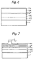
- a GaAs buried layer 7 is grown to bury opposite sides of the ridge portion.
- Fig. 4 is a diagram drawn on the basis of a photograph of a cross-sectional surface of the GaAs buried layer in the ridge portion and its vicinity taken by scanning type electronic microscopy (SEM) from a sample having the GaAs buried layer 7 grown in the process already explained.
- SEM scanning type electronic microscopy
- Fig. 5 shows a GaN semiconductor laser having a buried ridge structure according to the first embodiment of the invention.
- This GaN semiconductor laser has a SCH (Separate Confinement Heterostructure) configuration.
- a c-plane sapphire substrate 11 having the thickness of 400 ⁇ m for example, via an undoped GaN buffer layer 12, an n-type GaN contact layer 13, n-type AlGaN cladding layer 14, n-type GaN optical guide layer 15, active layer 16 having an undoped Ga 1-x In x N/Ga 1-y In y N multi-quantum well structure, for example, p-type GaN optical guide layer 17, p-type AlGaN cladding layer 18 and p-type GaN contact layer 19 are sequentially stacked.
- the GaN buffer layer 12 is 30 nm thick, for example.
- the n-type GaN contact layer 13 is 4 ⁇ m thick, for example, and doped with silicon (Si), for example, as the n-type impurity.
- the n-type AlGaN cladding layer 14 is 0.7 ⁇ m thick, for example, and doped with Si, for example, as the n-type impurity.
- the n-type GaN optical guide layer 15 is 0.1 ⁇ m thick, for example, and doped with Si, for example, as the n-type impurity.
- each well layer is 3 nm thick, and each barrier layer is 4 nm thick, for example.
- the p-type GaN optical guide layer 17 is 0.1 ⁇ m, for example, and doped with magnesium (Mg), for example, as the p-type impurity.
- the p-type AlGaN cladding layer 18 is 0.7 ⁇ m thick, for example, and doped with Mg, for example, as the p-type impurity.
- the p-type GaN contact layer 19 is 0.3 ⁇ m thick, for example, and doped with Mg, for example, as the p-type impurity.
- the upper portion of the n-type GaN contact layer 13, n-type AlGaN cladding layer 14, n-type GaN optical guide layer 15, active layer 16, p-type GaN optical guide layer 17 and p-type AlGaN cladding layer 18 have a mesa configuration of a predetermined width.
- the upper portion of the p-type AlGaN cladding layer 18 and the p-type GaN contact layer 19 form a ridge portion of a predetermined width, which extends in one direction.
- This expending direction of the ridge portion is the ⁇ 11-20 ⁇ direction, for example, and the width is 4 ⁇ m, for example.
- an undoped GaAs buried layer 20 is buried.
- the GaAs buried layer 20 has the [111] orientation.
- the p-side electrode 21 lies on the p-type GaN contact layer 19 in the ridge portion and the GaAs buried layer 20 at opposite sides thereof.
- the p-side electrode 21 has a Ni/Pt/Au structure made by sequentially stacking a Ni film, Pt film and Au film, for example, and these Ni film, Pt film and Au film are 10 nm thick, 100 nm thick and 300 nm thick, respectively, for example. Since the GaAs buried layer 20 has a high resistance, although the p-side electrode contacts both the p-type GaN contact layer 19 and the GaAs buried layer 20, the current flows only in the ridge stripe portion.
- the n-side electrode 22 lies on the n-type GaN contact layer 13 in the region adjacent to the mesa portion.
- This n-side electrode 22 has a Ti/Al/Pt/Au structure made by sequentially stacking a Ti film, Al film, Pt film and Au film, for example, and these Ti film, Al film, Pt film and Au film are 10 nm thick, 100 nm thick, 100 nm thick, and 300 nm thick, respectively, for example.
- the undoped GaN buffer layer 12 is grown by MOCVD at a temperature around 520 °C, for example.
- the substrate temperature is raised to a predetermined growth temperature, and the n-type GaN contact layer 13, n-type AlGaN cladding layer 14, n-type GaN optical guide layer 15, active layer 16 having the undoped Ga 1-x In x N/Ga 1-y In y N multi-quantum well structure, for example, p-type GaN optical guide layer 17, p-type AlGaN cladding layer 18 and p-type GaN contact layer 19 are sequentially stacked.
- the growth temperature is fixed at approximately 1000 °C.
- the growth temperature is fixed at approximately 800 °C.
- Used as source materials for growth of these GaN semiconductor layers are, for example, trimethyl gallium ((CH 3 ) 3 Ga, TMG) as the source material of a group III element, Ga, trimethyl aluminum ((CH 3 ) 3 Al, TMA) as the source material of a group III element, Al, trimethyl indium ((CH 3 ) 3 In, TMI) as the source material of a group III element, In, and ammonium (NH 3 ) as the source material of a group V element, N.
- Used as the carrier gas is a mixed gas of hydrogen (H 2 ) and nitrogen (N 2 ), for example.
- monosilane (SiH 4 ) is used as the n-type dopant
- bis-methyl cyclopentadienile magnesium ((CH 3 C 5 H 4 ) 2 Mg) or bis-cyclopentadienile magnesium ((C 5 H 5 ) 2 Mg) is used as the p-type dopant, for example.
- the c-plane sapphire substrate 11 having the GaN semiconductor layers grown thereon is taken out from the MOCVD apparatus.
- the SiO 2 film 23 having the thickness of 0.4 ⁇ m, for example, is stacked on the entire surface of the p-type GaN contact layer 19 by CVD, vacuum evaporation or sputtering, for example.
- a resist pattern (not shown) of a predetermined pattern is formed on the SiO 2 film 23 by lithography, and using the resist pattern as a mask, the SiO 2 film 23 is etched into the form of a stripe by wet etching using an etchant based on fluoric acid, for example, or RIE using an etching gas containing fluorine such CF 4 or CHF 3 , for example.
- etching is conducted to a predetermined depth in the thickness direction of the p-type AlGaN cladding layer 18 by RIE, for example, to make a ridge portion.
- RIE used as the etching gas of RIE is a chlorine-based gas, for example.
- the GaAs buried layer 20 is grown to bury opposite sides of the ridge portion.
- GaAs does not grow on the SiO 2 film 23, and selective growth of the GaAs buried layer 20 at opposite sides of the ridge portion is possible.
- Used as source materials for growth of the GaAs buried layer 20 are, for example, trimethyl gallium ((CH 3 ) 3 Ga, TMG) as the source material of a group III element, Ga, and arsine (AsH3) as the source material of a group V element, As.
- the c-plane sapphire substrate 11 having the GaAs buried layer 20 grown thereon is taken out from the MOCVD apparatus. Then, after the SiO 2 film 23 is removed by etching, a SiO 2 film 24 having a predetermined pattern is formed on the substrate surface in the same process as explained above, as shown in Fig. 9.
- etching is conducted by RIE, for example, to the depth exposing the n-type GaN contact layer 13 to pattern the upper part of the n-type GaN contact layer 13, n-type AlGaN cladding layer 14, n-type GaN optical guide layer 15, and the active layer having the undoped Ga 1-x In x N/Ga 1-y In y N multi-quantum well structure, for example, p-type GaN optical guide layer 17, p-type AlGaN cladding layer 18 and GaAs buried layer 20 into a mesa configuration.
- the SiO 2 film 24 is removed by etching. Then, a resist pattern (not shown) having a predetermined pattern is formed on the substrate surface, and a Ti film, Al film, Pt film and Au film are sequentially stacked on the entire substrate surface by vacuum evaporation, for example. Thereafter, the resist pattern is removed together with the overlying Ti film, Al film, Pt film and Au film (lift-off). As a result, as shown in Fig. 11, the n-side electrode 22 is formed on the n-type GaN contact layer 13 in the region adjacent to the mesa portion. After that, an alloying process is conducted to bring the n-side electrode 22 into ohmic contact.
- the p-side electrode 21 is formed on the p-type GaN contact layer 19 and the GaAs buried layer 20 at opposite sides thereof in the mesa portion. Thereafter, alloying is conducted to bring the p-side electrode 21 into ohmic contact.
- each bar is divided into chips by cleavage, for example.
- the intended GaN semiconductor laser having the buried ridge structure and the SCH structure as shown in Fig. 5 is obtained.
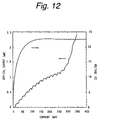
- Fig. 12 shows a result of measurement about optical output-electric current property and voltage-current property of the GaN semiconductor laser according to the first embodiment.
- a current of pulses having the pulse width of 5 ⁇ sec was applied at 1 msec intervals. It is noted from Fig. 12 that, as from the current value around 280 mA, the optical output suddenly rose and laser oscillation was certainly attained.
- the contact area between the p-side electrode 21 and the underlying semiconductor layer can be increased by burying the ridge with the GaAs buried layer 20, it is possible to promote dissipation of heat generated during operation, thereby prevent an increase of the current while the power is supplied, and increase the lifetime of the semiconductor laser.
- the growth temperature of the GaAs buried layer 20 is lower than the growth temperature of the active layer 16, the active layer 16 is not adversely affected by heat upon the growth of the GaAs buried layer 20.
- the band gap of the GaAs buried layer 20 is smaller than that of the active layer 16, the GaAs buried layer 20 functions as a light absorbing layer. Therefore, this semiconductor laser forms a loss-guided semiconductor laser stable in transverse modes, and can suppress higher mode oscillation upon a high output power.
- the following advantages are obtained as well. That is, since it is the problem with growth of GaN semiconductors, in general, that p-type impurities (acceptors) in the grown layers are inactivated by hydrogen in the growth atmosphere and post-annealing in a nitrogen atmosphere is indispensable after growth of p-type layers.
- the GaAs buried layer 20 or SiO 2 film 23 comes to the outermost surface during growth of the GaAs buried layer 23, hydrogen in the growth atmosphere does not directly attack p-type layers, and hydrogen, which may be taken into p-type layers during the first epitaxial growth process for growing layers up to the p-type GaN contact layer 19, tends to come off through the GaAs buried layer 20 or SiO 2 film 23. Therefore, p-type impurities in p-type layers can be activated during growth of the GaAs buried layer 20 without the need for post-annealing.
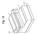
- Fig. 13 shows a GaN semiconductor laser having a buried ridge structure according to the second embodiment of the invention.
- the GaN semiconductor laser has a SCH structure.
- the AlGaAs buried layer 25 is [111]-oriented.
- the GaN semiconductor laser shown here is the same as the first embodiment, and explanation thereof is omitted.
- the GaN semiconductor laser according to the second embodiment can be manufactured by substantially the same manufacturing method used for manufacturing the GaN semiconductor laser according to the first embodiment.
- used as source materials for growth of the AlGaAs buried layer 25 are, for example, trimethyl aluminum ((CH 3 ) 3 Al, TMA) as the source material of a group III element, Al, trimethyl gallium ((CH 3 ) 3 Ga, TMG) as the source material of a group III element, Ga, and arsine (AsH 3 ) as the source material of a group V element, As.
- the contact area between the p-side electrode 21 and the underlying semiconductor layer can be increased by burying the ridge with the AlGaAs buried layer 25, it is possible to promote dissipation of heat generated during operation, like the first embodiment, thereby prevent an increase of the current while the power is supplied, and increase the lifetime of the semiconductor laser.
- the growth temperature of the AlGaAs buried layer 25 is lower than the growth temperature of the active layer 16, the active layer 16 is not adversely affected by heat upon the growth of the AlGaAs buried layer 25.
- the band gap of the AlGaAs buried layer 25 is smaller than that of the active layer 16, the AlGaAs buried layer 25 functions as a light absorbing layer.
- this semiconductor laser forms a loss-guided semiconductor laser stable in transverse modes, and can suppress higher mode oscillation upon a high output power, especially because the difference in refractive index between the ridge portion and its outside portion can be controlled more easily by changing the Al composition of the AlGaAs buried layer 25.
- the second embodiment is the same as the first embodiment also in enabling activation of p-type impurities in p-type layers during growth of the AlGaAs buried layer 25 without the need for post-annealing.
- Fig. 14 shows a GaN semiconductor laser having a buried ridge structure according to the third embodiment of the invention.
- the GaN semiconductor laser has a SCH structure.
- a (Al x Ga 1-x ) y In 1-y P buried layer 26 is buried at opposite sides of the ridge portion.
- the (Al x Ga 1-x ) y In 1-y P buried layer 26 is [111]-oriented.
- the GaN semiconductor laser shown here is the same as the first embodiment, and explanation thereof is omitted.
- the GaN semiconductor laser according to the third embodiment can be manufactured by substantially the same manufacturing method used for manufacturing the GaN semiconductor laser according to the first embodiment, except that the (Al x Ga 1-x ) y In 1-y P buried layer 26 is grown at a growth temperature of 500°C through 800°C.
- Used here as source materials for growth of the (Al x Ga 1-x ) y In 1-y P buried layer 26 are, for example, trimethyl aluminum ((CH 3 ) 3 Al, TMA) as the source material of a group III element, Al, trimethyl gallium ((CH 3 ) 3 Ga, TMG) as the source material of a group III element, Ga, trimethyl indium ((CH 3 ) 3 In, TMI) as the source material of a group III element, and phosphine (PH 3 ) as the source material of a group V element, P.
- trimethyl aluminum ((CH 3 ) 3 Al, TMA) as the source material of a group III element
- Al trimethyl gallium
- (CH 3 ) 3 Ga, TMG) as the source material of a group III element
- Ga trimethyl indium ((CH 3 ) 3 In, TMI) as the source material of a group III element
- phosphine (PH 3 ) phosphine
- the contact area between the p-side electrode 21 and the underlying semiconductor layer can be increased by burying the ridge with the (Al x Ga 1-x ) y In 1-y P buried layer 26, it is possible to promote dissipation of heat generated during operation, like the first embodiment, thereby prevent an increase of the current while the power is supplied, and increase the lifetime of the semiconductor laser. Additionally, since the growth temperature of the (Al x Ga 1-x ) y In 1-y P buried layer 26 is lower than the growth temperature of the active layer 16, the active layer 16 is not adversely affected by heat upon the growth of the (Al x Ga 1-x ) y In 1-y P buried layer 26.
- the band gap of the (Al x Ga 1-x ) y In 1-y P buried layer 26 is smaller than that of the active layer 16, the (Al x Ga 1-x ) y In 1-y P buried layer 26 functions as a light absorbing layer. Therefore, this semiconductor laser forms a loss-guided semiconductor laser stable in transverse modes, and can suppress higher mode oscillation upon a high output power, especially because the difference in refractive index between the ridge portion and its outside portion can be controlled more easily by changing the composition of the (Al x Ga 1-x ) y In 1-y P buried layer 26.
- the third embodiment is the same as the first embodiment also in enabling activation of p-type impurities in p-type layers during growth of the (Al x Ga 1-x ) y In 1-y P buried layer 26 without the need for post-annealing.
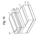
- Fig. 15 shows a GaN semiconductor laser having a buried ridge structure according to the fourth embodiment of the invention.
- the GaN semiconductor laser has a SCH structure.
- a Zn x Mg 1-x S y Se 1-y buried layer 27 is buried at opposite sides of the ridge portion.
- the Zn x Mg 1-x S y Se 1-y buried layer 27 is [111]-oriented.
- the GaN semiconductor laser shown here is the same as the first embodiment, and explanation thereof is omitted.
- the GaN semiconductor laser according to the fourth embodiment can be manufactured by substantially the same manufacturing method used for manufacturing the GaN semiconductor laser according to the first embodiment, except that the Zn x Mg 1-x S y Se 1-y buried layer 27 is grown at a growth temperature of 300°C through 600°C by MOCVD.
- DMZn dimethyl zinc
- Zn bis-methyl cyclopentadienile magnesium
- C 5 H 5 ) 2 Mg bis-cyclopentadienile magnesium
- Mg diethyl phosphine
- DMSe dimethyl selenium
- the contact area between the p-side electrode 21 and the underlying semiconductor layer can be increased by burying the ridge with the Zn x Mg 1-x S y Se 1-y buried layer 27, it is possible to promote dissipation of heat generated during operation, like the first embodiment, thereby prevent an increase of the current while the power is supplied, and increase the lifetime of the semiconductor laser. Additionally, since the growth temperature of the Zn x Mg 1-x S y Se 1-y buried layer 27 is lower than the growth temperature of the active layer 16, the active layer 16 is not adversely affected by heat upon the growth of the Zn x Mg 1-x S y Se 1-y buried layer 27.
- the Zn x Mg 1-x S y Se 1-y buried layer 27 functions as a light absorbing layer. Therefore, this semiconductor laser forms a loss-guided semiconductor laser stable in transverse modes, and can suppress higher mode oscillation upon a high output power, especially because the difference in refractive index between the ridge portion and its outside portion can be controlled more easily by changing the composition of the Zn x Mg 1-x S y Se 1-y buried layer 27.
- the fourth embodiment is the same as the first embodiment also in enabling activation of p-type impurities in p-type layers during growth of the Zn x Mg 1-x S y Se 1-y buried layer 27 without the need for post-annealing.
- the numerical values, structures, substrates, source materials and processes proposed with reference to the first to fourth embodiments are not but examples, and any other appropriate numerical values, structures, substrates, source materials and processes may be used.
- the ridge stripe has been explained as extending in the ⁇ 11-20 ⁇ direction of the c-plane sapphire substrate 1, but it may extend in the ⁇ 1-100 ⁇ direction, instead.
- any of SiC substrate, Si substrate and spinel substrate is usable is so desired.
- the first to fourth embodiments have been explained as applying the invention to SCH-structured GaN semiconducgtor lasers; however, the invention is also applicable, needless to say, to GaN semiconductor lasers having a DH (double heterostructure) configuration, and also to electron transport devices such as FET, which use nitride III-V compound semiconductors.
- the semiconductor laser proposed according to the invention in which opposite sides of the ridge-shaped stripe are buried with the buried semiconductor layer made of Al x Ga 1-x As (0 ⁇ x ⁇ 1), (Al x Ga 1-x ) y In 1-y P (0 ⁇ x ⁇ 1, 0 ⁇ y ⁇ 1) or Zn x Mg 1-x S y Se 1-y (0 ⁇ x ⁇ 1, 0 ⁇ y ⁇ 1), can stably control transverse modes and thereby minimize higher-mode oscillation upon a high output power, and it is excellent in heat dissipation.
- the manufacturing method of a semiconductor laser according to the invention can readily manufacture the above-mentioned semiconductor laser by making a ridge-shaped stripe and growing a buried semiconductor layer made of Al x Ga 1-x As (0 ⁇ x ⁇ 1), (Al x Ga 1-x ) y In 1-y P (0 ⁇ x ⁇ 1, 0 ⁇ y ⁇ 1) or Zn x Mg 1-x S y Se 1-y (0 ⁇ x ⁇ 1, 0 ⁇ y ⁇ 1) to bury opposite sides of the ridge-shaped stripe.
- the semiconductor laser can be manufactured more easily. Moreover, by burying the buried semiconductor layer at a lower growth temperature than the growth temperature of the active layer, thermal deterioration of the active layer can be prevented, and a semiconductor laser having a long lifetime can be manufactured.
- the semiconductor device in which the portion around the projection is buried with the buried semiconductor layer made of Al x Ga 1-x As (0 ⁇ x ⁇ 1), (Al x Ga 1-x ) y In 1-y P (0 ⁇ x ⁇ 1, 0 ⁇ y ⁇ 1) or Zn x Mg 1-x S y Se 1-y (0 ⁇ x ⁇ 1, 0 ⁇ y ⁇ 1), in the case where the projection becomes a heat generating source, heat dissipation from the ridge portion is promoted, and this minimizes deterioration of the device and elongates the lifetime of the semiconductor device.
- the manufacturing method of a semiconductor device according to the invention can readily manufacture the above-mentioned semiconductor device. Especially when using metal organic chemical vapor deposition for growth of the buried semiconductor layer, selective growth is possible, and the semiconductor device can be manufactured more easily.
Landscapes
- Physics & Mathematics (AREA)
- Optics & Photonics (AREA)
- Engineering & Computer Science (AREA)
- Condensed Matter Physics & Semiconductors (AREA)
- General Physics & Mathematics (AREA)
- Electromagnetism (AREA)
- Nanotechnology (AREA)
- Chemical & Material Sciences (AREA)
- Biophysics (AREA)
- Crystallography & Structural Chemistry (AREA)
- Life Sciences & Earth Sciences (AREA)
- Geometry (AREA)
- Semiconductor Lasers (AREA)
- Led Devices (AREA)
Applications Claiming Priority (2)
| Application Number | Priority Date | Filing Date | Title |
|---|---|---|---|
| JP11680499A JP3735638B2 (ja) | 1999-04-23 | 1999-04-23 | 半導体レーザおよびその製造方法 |
| JP11680499 | 1999-04-23 |
Publications (2)
| Publication Number | Publication Date |
|---|---|
| EP1047163A2 true EP1047163A2 (de) | 2000-10-25 |
| EP1047163A3 EP1047163A3 (de) | 2004-02-25 |
Family
ID=14696085
Family Applications (1)
| Application Number | Title | Priority Date | Filing Date |
|---|---|---|---|
| EP00108401A Withdrawn EP1047163A3 (de) | 1999-04-23 | 2000-04-17 | Halbleiterlaser, Halbleiterlaservorrichtung und Herstellungsverfahren |
Country Status (5)
| Country | Link |
|---|---|
| US (1) | US6577662B1 (de) |
| EP (1) | EP1047163A3 (de) |
| JP (1) | JP3735638B2 (de) |
| KR (1) | KR20000077066A (de) |
| TW (1) | TW484254B (de) |
Families Citing this family (8)
| Publication number | Priority date | Publication date | Assignee | Title |
|---|---|---|---|---|
| DE19963807A1 (de) * | 1999-12-30 | 2001-07-19 | Osram Opto Semiconductors Gmbh | Streifenlaserdiodenelement |
| JP2010245559A (ja) * | 2000-12-28 | 2010-10-28 | Sony Corp | 半導体発光素子の製造方法 |
| JP3864735B2 (ja) | 2000-12-28 | 2007-01-10 | ソニー株式会社 | 半導体発光素子およびその製造方法 |
| JP2002299763A (ja) * | 2001-04-03 | 2002-10-11 | Sony Corp | 半導体レーザ素子及びその作製方法 |
| DE60311678T2 (de) * | 2002-12-20 | 2007-11-22 | Cree, Inc. | Verfahren zur herstellung von halbleitervorrichtungen mit mesastrukturen und vielfachen passivierungsschichten und verwandte vorrichtungen |
| JP2005093726A (ja) * | 2003-09-17 | 2005-04-07 | Toshiba Corp | 半導体レーザ素子、半導体レーザ素子の製造方法 |
| GB2411520A (en) * | 2004-02-25 | 2005-08-31 | Agilent Technologies Inc | Method of forming laser mesa by reactive ion etching followed by in situ etching in regrowth reactor |
| US9524869B2 (en) * | 2004-03-11 | 2016-12-20 | Epistar Corporation | Nitride-based semiconductor light-emitting device |
Family Cites Families (7)
| Publication number | Priority date | Publication date | Assignee | Title |
|---|---|---|---|---|
| JP2809691B2 (ja) * | 1989-04-28 | 1998-10-15 | 株式会社東芝 | 半導体レーザ |
| US5383211A (en) * | 1993-11-02 | 1995-01-17 | Xerox Corporation | TM-polarized laser emitter using III-V alloy with nitrogen |
| JPH08195522A (ja) * | 1994-11-16 | 1996-07-30 | Hitachi Ltd | 半導体レーザ |
| JP3905935B2 (ja) * | 1995-09-01 | 2007-04-18 | 株式会社東芝 | 半導体素子及び半導体素子の製造方法 |
| JPH09237933A (ja) * | 1996-02-29 | 1997-09-09 | Mitsubishi Electric Corp | 半導体レーザ,及びその製造方法 |
| JPH09266352A (ja) * | 1996-03-28 | 1997-10-07 | Fuji Photo Film Co Ltd | 半導体発光素子 |
| JP3060973B2 (ja) * | 1996-12-24 | 2000-07-10 | 日本電気株式会社 | 選択成長法を用いた窒化ガリウム系半導体レーザの製造方法及び窒化ガリウム系半導体レーザ |
-
1999
- 1999-04-23 JP JP11680499A patent/JP3735638B2/ja not_active Expired - Fee Related
-
2000
- 2000-04-14 TW TW089107023A patent/TW484254B/zh not_active IP Right Cessation
- 2000-04-17 EP EP00108401A patent/EP1047163A3/de not_active Withdrawn
- 2000-04-19 US US09/552,498 patent/US6577662B1/en not_active Expired - Fee Related
- 2000-04-22 KR KR1020000021434A patent/KR20000077066A/ko not_active Abandoned
Also Published As
| Publication number | Publication date |
|---|---|
| JP3735638B2 (ja) | 2006-01-18 |
| TW484254B (en) | 2002-04-21 |
| EP1047163A3 (de) | 2004-02-25 |
| JP2000307193A (ja) | 2000-11-02 |
| US6577662B1 (en) | 2003-06-10 |
| KR20000077066A (ko) | 2000-12-26 |
Similar Documents
| Publication | Publication Date | Title |
|---|---|---|
| EP1387453B1 (de) | Halbleiterelement aus galliumnitridzusammensetzung | |
| US6680959B2 (en) | Semiconductor light emitting device and semiconductor laser | |
| US8587004B2 (en) | Semiconductor light emitting device, its manufacturing method, semiconductor device and its manufacturing method | |
| US6920166B2 (en) | Thin film deposition method of nitride semiconductor and nitride semiconductor light emitting device | |
| US20100317136A1 (en) | Method for producing semiconductor light emitting device, method for producing semiconductor device, method for producing device, method for growing nitride type iii-v group compound semiconductor layer, method for growing semiconductor layer, and method for growing layer | |
| JPH11135770A (ja) | 3−5族化合物半導体とその製造方法および半導体素子 | |
| CN101714745B (zh) | 半导体激光器及其制造方法、光拾波器和光盘驱动装置 | |
| US7893454B2 (en) | Method for producing structured substrate, structured substrate, method for producing semiconductor light emitting device, semiconductor light emitting device, method for producing semiconductor device, semiconductor device, method for producing device, and device | |
| EP1005123B1 (de) | Halbleiterlaser, Halbleitervorrichtung und Herstellungsverfahren | |
| US7755101B2 (en) | Semiconductor light emitting device | |
| US6577662B1 (en) | Semiconductor laser, and manufacturing method thereof, semiconductor device and manufacturing method thereof | |
| JP4826019B2 (ja) | 半導体レーザ素子の製造方法 | |
| JP3975971B2 (ja) | 半導体レーザの製造方法 | |
| JP2001210912A (ja) | 半導体レーザおよびその製造方法 | |
| JP2000164985A (ja) | 半導体レーザ | |
| JP2006013476A (ja) | 3−5族化合物半導体とその製造方法および半導体素子 | |
| JP2002111131A (ja) | 半導体発光素子およびその製造方法 |
Legal Events
| Date | Code | Title | Description |
|---|---|---|---|
| PUAI | Public reference made under article 153(3) epc to a published international application that has entered the european phase |
Free format text: ORIGINAL CODE: 0009012 |
|
| AK | Designated contracting states |
Kind code of ref document: A2 Designated state(s): AT BE CH CY DE DK ES FI FR GB GR IE IT LI LU MC NL PT SE |
|
| AX | Request for extension of the european patent |
Free format text: AL;LT;LV;MK;RO;SI |
|
| PUAL | Search report despatched |
Free format text: ORIGINAL CODE: 0009013 |
|
| RIC1 | Information provided on ipc code assigned before grant |
Ipc: 7H 01S 5/223 B Ipc: 7H 01S 5/22 B Ipc: 7H 01S 5/323 B Ipc: 7H 01S 5/343 A |
|
| AK | Designated contracting states |
Kind code of ref document: A3 Designated state(s): AT BE CH CY DE DK ES FI FR GB GR IE IT LI LU MC NL PT SE |
|
| AX | Request for extension of the european patent |
Extension state: AL LT LV MK RO SI |
|
| 17P | Request for examination filed |
Effective date: 20040804 |
|
| AKX | Designation fees paid |
Designated state(s): DE FR GB |
|
| STAA | Information on the status of an ep patent application or granted ep patent |
Free format text: STATUS: THE APPLICATION IS DEEMED TO BE WITHDRAWN |
|
| 18D | Application deemed to be withdrawn |
Effective date: 20060119 |