EP1047178B1 - Convertisseur continu-continu à résonance et sa méthode de commande - Google Patents
Convertisseur continu-continu à résonance et sa méthode de commande Download PDFInfo
- Publication number
- EP1047178B1 EP1047178B1 EP00108751A EP00108751A EP1047178B1 EP 1047178 B1 EP1047178 B1 EP 1047178B1 EP 00108751 A EP00108751 A EP 00108751A EP 00108751 A EP00108751 A EP 00108751A EP 1047178 B1 EP1047178 B1 EP 1047178B1
- Authority
- EP
- European Patent Office
- Prior art keywords
- voltage
- converter
- resonant
- transition
- level signal
- Prior art date
- Legal status (The legal status is an assumption and is not a legal conclusion. Google has not performed a legal analysis and makes no representation as to the accuracy of the status listed.)
- Expired - Lifetime
Links
Images

Classifications
-
- H—ELECTRICITY
- H02—GENERATION; CONVERSION OR DISTRIBUTION OF ELECTRIC POWER
- H02M—APPARATUS FOR CONVERSION BETWEEN AC AND AC, BETWEEN AC AND DC, OR BETWEEN DC AND DC, AND FOR USE WITH MAINS OR SIMILAR POWER SUPPLY SYSTEMS; CONVERSION OF DC OR AC INPUT POWER INTO SURGE OUTPUT POWER; CONTROL OR REGULATION THEREOF
- H02M3/00—Conversion of DC power input into DC power output
- H02M3/22—Conversion of DC power input into DC power output with intermediate conversion into AC
- H02M3/24—Conversion of DC power input into DC power output with intermediate conversion into AC by static converters
- H02M3/28—Conversion of DC power input into DC power output with intermediate conversion into AC by static converters using discharge tubes with control electrode or semiconductor devices with control electrode to produce the intermediate AC
- H02M3/325—Conversion of DC power input into DC power output with intermediate conversion into AC by static converters using discharge tubes with control electrode or semiconductor devices with control electrode to produce the intermediate AC using devices of a triode or a transistor type requiring continuous application of a control signal
- H02M3/335—Conversion of DC power input into DC power output with intermediate conversion into AC by static converters using discharge tubes with control electrode or semiconductor devices with control electrode to produce the intermediate AC using devices of a triode or a transistor type requiring continuous application of a control signal using semiconductor devices only
- H02M3/33561—Conversion of DC power input into DC power output with intermediate conversion into AC by static converters using discharge tubes with control electrode or semiconductor devices with control electrode to produce the intermediate AC using devices of a triode or a transistor type requiring continuous application of a control signal using semiconductor devices only having more than one ouput with independent control
-
- H—ELECTRICITY
- H02—GENERATION; CONVERSION OR DISTRIBUTION OF ELECTRIC POWER
- H02M—APPARATUS FOR CONVERSION BETWEEN AC AND AC, BETWEEN AC AND DC, OR BETWEEN DC AND DC, AND FOR USE WITH MAINS OR SIMILAR POWER SUPPLY SYSTEMS; CONVERSION OF DC OR AC INPUT POWER INTO SURGE OUTPUT POWER; CONTROL OR REGULATION THEREOF
- H02M3/00—Conversion of DC power input into DC power output
- H02M3/22—Conversion of DC power input into DC power output with intermediate conversion into AC
- H02M3/24—Conversion of DC power input into DC power output with intermediate conversion into AC by static converters
- H02M3/28—Conversion of DC power input into DC power output with intermediate conversion into AC by static converters using discharge tubes with control electrode or semiconductor devices with control electrode to produce the intermediate AC
- H02M3/325—Conversion of DC power input into DC power output with intermediate conversion into AC by static converters using discharge tubes with control electrode or semiconductor devices with control electrode to produce the intermediate AC using devices of a triode or a transistor type requiring continuous application of a control signal
- H02M3/335—Conversion of DC power input into DC power output with intermediate conversion into AC by static converters using discharge tubes with control electrode or semiconductor devices with control electrode to produce the intermediate AC using devices of a triode or a transistor type requiring continuous application of a control signal using semiconductor devices only
-
- Y—GENERAL TAGGING OF NEW TECHNOLOGICAL DEVELOPMENTS; GENERAL TAGGING OF CROSS-SECTIONAL TECHNOLOGIES SPANNING OVER SEVERAL SECTIONS OF THE IPC; TECHNICAL SUBJECTS COVERED BY FORMER USPC CROSS-REFERENCE ART COLLECTIONS [XRACs] AND DIGESTS
- Y02—TECHNOLOGIES OR APPLICATIONS FOR MITIGATION OR ADAPTATION AGAINST CLIMATE CHANGE
- Y02B—CLIMATE CHANGE MITIGATION TECHNOLOGIES RELATED TO BUILDINGS, e.g. HOUSING, HOUSE APPLIANCES OR RELATED END-USER APPLICATIONS
- Y02B70/00—Technologies for an efficient end-user side electric power management and consumption
- Y02B70/10—Technologies improving the efficiency by using switched-mode power supplies [SMPS], i.e. efficient power electronics conversion e.g. power factor correction or reduction of losses in power supplies or efficient standby modes
Definitions
- the present invention relates to a resonant-transition dc-to-dc converter, and to a method of controlling the resonant transition of a dc-to-dc converter.
- the present invention may be used to advantage, though not exclusively, in flyback and boost resonant-transition dc-to-dc converters, to which the following description refers purely by way of example.
- circuits comprising linear power supplies, i.e. in which the transistors operate permanently in the linear region.
- One proposed solution is to use supply circuits comprising switching dc-to-dc converters featuring inductive components, the charging and discharging of which are controlled by active components defined by control transistors switching between a saturation and a cutoff condition (on/off).
- switching losses - In switching dc-to-dc converters, the power dissipated during switching - also known as switching losses - is directly proportional to the switching frequency of the active components, which therefore cannot be so high as to result in switching losses making the use of such power supply circuits unfeasible.
- This technique also calls for a discharge circuit to discharge the capacitive element completely when the control transistor is cut off, so that, the instant the control transistor switches to the saturation state, the voltage at its terminals is substantially zero and the switching losses therefore greatly reduced. More detailed information about the Snubber technique is also to be found, for example, in the text mentioned above.
- control transistors for charging and discharging the inductive and capacitive components are turned on or off when the current flowing in them or the voltage at their terminals is zero respectively.
- All known resonant-transition dc-to-dc converters have the drawback of having fairly complex circuit structures and employing a large number of additional components for detecting zero current flow in, or zero voltage at the terminals of, the control transistors.
- US-A-5 680 034 discloses a pulse width modulated (PWM) controller for resonant converters, which controls a zero-voltage switching resonant power converter or inverter.
- PWM pulse width modulated
- the on time of the power switch of the converter or inverter is varied by an error amplifier such that the output voltage of the converter or inverter maintains proportionality to a reference voltage.
- the off time is terminated by a switch-voltage detector when the voltage across the power switch (110) drops below a threshold voltage due to the natural resonance of the external resonating capacitor and inductors.
- a single timing capacitor is employed both for determining the on time and the off time.
- two timing capacitors are employed for separately determining the maximum allowed off time and the variable on time.
- a cycle-by-cycle current limit circuit comprising a current sensor, a comparator, and an R-S latch may be added to the circuits representing each of the embodiments.
- a soft start subcircuit and an overlap detector protection against overdissipation of the power switch caused by loss of zero-voltage switching can also be implemented.
- the soft start subcircuit can also be triggered by a voltage detector, which monitors the output voltage of the power converter or some other voltage within the system, such as the peak voltage across the power switch (110), to effectively implement overvoltage protection.
- the present invention is based on the principle of only switching the control transistor from the cutoff to the saturation condition when the Snubber capacitor is discharged naturally and the voltage at its terminals is therefore substantially zero.
- the voltage at the terminals of the Snubber capacitor is measured directly, and the control transistor is only switched from the cutoff to the saturation condition when the measured voltage is less than or equal to a predetermined threshold value close to zero.
- Number 1 in Figure 1 indicates as a whole a flyback resonant-transition dc-to-dc converter in accordance with a first embodiment of the present invention.
- Converter 1 comprises a first and a second input terminal 2, 4 connected respectively, in use, to the positive and negative poles of an electrical energy source 6, e.g. a battery, supplying a supply voltage VB; and a number of pairs of output terminals (only two shown in Figure 1 ), each comprising a first and a second output terminal 8, 10, between which is connected, in use, a respective load represented in Figure 1 by a resistor 12.
- an electrical energy source 6 e.g. a battery, supplying a supply voltage VB
- a number of pairs of output terminals each comprising a first and a second output terminal 8, 10, between which is connected, in use, a respective load represented in Figure 1 by a resistor 12.
- Converter 1 comprises a stabilizing capacitor 20 connected between first and second input terminals 2, 4; a transformer 22 comprising a primary winding 24 interposed between first and second input terminals 2, 4, and a number of secondary windings 26, each connected to a respective pair of output terminals 8, 10 via a diode 14 and a capacitor 16, as described later on; a bipolar or MOSFET control transistor 28 - bipolar in the example shown - in series with primary winding 24; a Snubber capacitor 30 in parallel with control transistor 28; a first comparator circuit 32 in parallel with Snubber capacitor 30; a second comparator circuit 34 in series with control transistor 28; and a control circuit 36 for controlling control transistor 28.
- primary winding 24 has a first terminal connected to first input terminal 2 of converter 1; and a second terminal connected to the collector terminal of control transistor 28, which has the emitter terminal connected to second input terminal 4 of converter 1 via second comparator circuit 34, and the base terminal receiving a logic control signal T, which, at a high logic value, turns on control transistor 28 (which can be likened to a closed switch), and, at a low logic value, turns off control transistor 28 (which can be likened to an open switch).
- Each secondary winding 26 has a first terminal connected to the respective first output terminal 8 of converter 1 via respective diode 14; and a second terminal connected directly to the respective second output terminal 10.
- Each diode 14 has an anode terminal connected to the first terminal of secondary winding 26, and a cathode terminal connected to output terminal 8; and each capacitor 16 is connected between respective output terminals 8, 10.
- the first comparator circuit 32 has a first and second input terminal connected to the terminals of Snubber capacitor 30; and an output terminal supplying a logic voltage level signal VS1, which assumes a high logic level when the voltage at the terminals of Snubber capacitor 30 is less than or equal to a first predetermined threshold value VTH1, and a low logic level when the voltage at the terminals of Snubber capacitor 30 is greater than first threshold value VTH1.
- the first threshold value VTH1 conveniently ranges between zero and ten percent of the supply voltage VB supplied by electrical energy source 6. Obviously, the closer the first threshold value VTH1 is to zero, the lower the switching losses will be.
- the second comparator circuit 34 has a first input terminal connected to the emitter terminal of control transistor 28; a second input terminal connected to the second input terminal 4 of converter 1; and an output terminal supplying a logic current level signal IS, which assumes a high logic level when the current flow in control transistor 28, and hence in primary winding 24, is greater than or equal to a second predetermined threshold value ITH, and a low logic level when the current is less than the second threshold value ITH.
- the second threshold value ITH depends on the power requested of converter 1 and, in particular, increases alongside an increase in the difference between the desired output voltage and the actual output voltage. As such, when the output voltage of the converter tends to fall, due an increase in load, the second threshold value ITH increases in an attempt to compensate for the fall in output voltage.
- Control circuit 36 has a first and second input terminal connected respectively to, and receiving voltage level signal VS1 and current level signal IS from, the output terminals of first and second comparator circuits 32, 34; and an output terminal supplying control signal T for control transistor 28.
- control signal T switches from a low to a high logic state, corresponding to turn-on of control transistor 28, when voltage level signal VS1 switches from a low to a high logic level, i.e. when the voltage at the terminals of Snubber capacitor 30 is less than or equal to first threshold value VTH1; and switches from a high to a low logic state, corresponding to turn-off of control transistor 28, when current level signal IS switches from a low to a high logic level, i.e. when the current flow in primary winding 24 of transformer 22 is greater than or equal to second threshold value ITH.
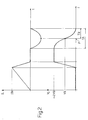
- control transistor 28 is cut off, Snubber capacitor 30 is discharged, and voltage VC and current IL are both zero.
- a closed loop is thus formed comprising electrical energy source 6, primary winding 24 of transformer 22, control transistor 28 and second comparator circuit 34, and a current IL increasing linearly in time flows in primary winding 24 of transformer 22 to store energy in the core of transformer 22, while the voltage VC at the terminals of Snubber capacitor 30 remains substantially nil.
- a closed loop comprising electrical energy source 6, primary winding 24 of transformer 22, Snubber capacitor 30 and second comparator circuit 34, and the dc-to-dc converter operates in the following three steps:
- control signal T generated by control circuit 36 switches from a low to a high logic state, thus turning control transistor 28 back on.
- Control transistor 28 switches from off to on at substantially zero voltage, so that the switching losses are extremely small.
- Figure 3 shows a flyback resonant-transition dc-to-dc converter in accordance with a second embodiment of the present invention, which is similar to dc-to-dc converter 1 and therefore only described below insofar as it differs from dc-to-dc converter 1, and using the same reference numbers for any parts identical with or corresponding to those already described.
- the second embodiment of the present invention is based on the principle of detecting the instant in which the voltage at the terminals of Snubber capacitor 30 is zeroed, by measuring an electric quantity correlated to the voltage at the terminals of Snubber capacitor 30, as opposed to measuring the voltage itself.
- Figure 3 shows a circuit diagram of a flyback resonant-transition dc-to-dc converter in accordance with a second embodiment of the present invention.
- the Figure 3 dc-to-dc converter differs from dc-to-dc converter 1 by the first comparator circuit, indicated 32', being connected in parallel with one of secondary windings 26, as opposed to Snubber capacitor 30, to detect the voltage between the terminals of secondary winding 26, which voltage is correlated, via the transformation ratio of transformer 22, to the voltage in primary winding 24 of transformer 22.
- first comparator circuit 32' is connected directly to the terminals of secondary winding 26 upstream from diode 14, and generates at the output terminal a logic voltage level signal VS2, which assumes a high logic level when the voltage VA in secondary winding 26 is less than or equal to a third predetermined threshold value VTH2, and a low logic level when the voltage VA in secondary winding 26 is greater than third threshold value VTH2.
- Third threshold value VTH2 conveniently ranges between zero and ten percent of the supply voltage VB supplied by electrical energy source 6 and referred back to secondary winding 26, taking into account the transformation ratio of transformer 22.
- Dc-to-dc converter 1' also comprises a delay circuit 38 interposed between first comparator circuit 32' and control circuit 36 to generate a delayed level signal VSR obtained by so delaying second voltage level signal VS2 that the switching edge from the low to high logic level of the delayed voltage level signal VSR occurs when the voltage at the terminals of Snubber capacitor 30 is less than or equal to first threshold value VTH1.
- second threshold value VTH2 assumes a zero value
- the delay introduced by delay circuit 38 equals the aforementioned time TB
- the delay introduced by delay circuit 38 is correlated to the value assumed by second threshold value VTH2 and, since the current flow pattern in primary winding 24 of transformer 22 is known, can be calculated easily.
- Converter 1' operates in the same way as dc-to-dc converter 1 already described.
- converters 1, 1' As compared with known flyback resonant-transition converters employing the Snubber technique to reduce switching losses, the circuit structure of converters 1, 1' is much simpler by requiring only two additional comparator circuits having a substantially negligible effect on the final cost of the converters.
- one of secondary windings 26 of converter 1' in the second embodiment need not be connected to a respective pair of output terminals 8, 10 of converter 1', and hence to a load, and may be used exclusively for determining the voltage VA at the terminals of the secondary windings; in which case, only first comparator circuit 32' would be connected to the terminals of said secondary winding.
- the instant in which the current flowing in primary winding 24 of transformer 22 is greater than or equal to the third threshold value may be detected otherwise than as described, and in particular also by detecting a voltage.
Landscapes
- Engineering & Computer Science (AREA)
- Power Engineering (AREA)
- Dc-Dc Converters (AREA)
Claims (11)
- Convertisseur continu-continu (courant continu) à résonance-transition (1) comportant des première et seconde bornes d'entrée (2, 4) destinées à être connectées, en utilisation, à une source d'énergie électrique (6), au moins des première et seconde bornes de sortie (8, 10) destinées à être connectées, en utilisation, à une charge (12), un transformateur (22) comportant un enroulement primaire (24) connecté entre lesdites première et seconde bornes d'entrée (2, 4), et au moins un enroulement secondaire (26) connecté entre lesdites première et seconde bornes de sortie (8, 10), un commutateur commandé (28) connecté entre ledit enroulement primaire (24) et l'une desdites première et seconde bornes (2,4) et ayant une borne de commande configurée pour recevoir un signal de commande logique (T) ayant un premier bord de commutation pour fermer ledit commutateur commandé (28) et un second bord de commutation pour ouvrir ledit commutateur commandé (28), des moyens capacitifs (30) connectés en parallèle avec ledit commutateur commandé (28), des moyens d'indication de niveau de tension (32 ; 32', 38) configurés pour détecter une quantité électrique associée à une tension (VC) à travers lesdits moyens capacitifs (30) et générer un premier signal de niveau de tension logique (VS1 ; VSR) ayant un bord de commutation lorsque ladite tension (VC) à travers lesdits moyens capacitifs (30) est inférieure ou égale à une tension de seuil (VTH1 ; VTH2), et des moyens de commande (36) configurés pour recevoir ledit premier signal de niveau de tension (VS1 ; VSR) et générer ledit signal de commande (T) pour lesdits moyens de commutation commandés (28) et avec ledit premier bord de commutation généré en réponse audit bord de commutation dudit premier signal de niveau de tension (VS1 ; VSR), caractérisé en ce que ledit convertisseur continu-continu à résonance-transition (1) inclut en outre des moyens d'indication de niveau de courant (34) configurés pour détecter une quantité électrique associée à un courant circulant dans ledit enroulement primaire (24) dudit transformateur (22) et générer un signal de niveau de courant logique (IS) ayant un bord de commutation lorsque ledit courant est supérieur ou égal à un courant de seuil (ITH), et en ce que lesdits moyens de commande (36) sont en outre configurés pour recevoir également ledit signal de niveau de courant (IS) et générer ledit signal de commande (T) pour ledit commutateur commandé (28) et avec ledit second bord de commutation généré en réponse audit bord de commutation dudit signal de niveau de courant (IS).
- Convertisseur continu-continu à résonance-transition (1) selon la revendication 1, dans lequel ladite tension de seuil (VTH ; VTH2) est comprise de manière appropriée entre zéro et dix pourcents d'une quantité associée à une tension d'alimentation (VB) de ladite source d'énergie électrique (6).
- Convertisseur continu-continu à résonance-transition (1) selon la revendication 1 ou 2, dans lequel ledit courant de seuil (ITH) est fonction de la puissance demandée audit convertisseur (1).
- Convertisseur continu-continu à résonance-transition (1) selon l'une quelconque des revendications précédentes, dans lequel ledit courant de seuil (ITH) augmente en relation avec une augmentation de la différence entre une tension de sortie voulue et une tension de sortie réelle dudit convertisseur (1).
- Convertisseur continu-continu à résonance-transition (1) selon l'une quelconque des revendications précédentes, dans lequel lesdits moyens indiquant un niveau de courant comportent un comparateur de courant (34) connecté en série avec ledit enroulement primaire (24) dudit transformateur (22).
- Convertisseur continu-continu à résonance-transition (1) selon la revendication 1, dans lequel lesdits moyens d'indication de niveau de courant comportent un comparateur de tension (32) connecté en parallèle avec lesdits moyens capacitifs (30).
- Convertisseur continu-continu à résonance-transition (1) selon l'une quelconque des revendications précédentes 1 à 5, dans lequel lesdits moyens d'indication de niveau de tension comportent un comparateur de tension (32') configuré pour détecter une quantité électrique associée à une tension (VA) à travers ledit enroulement secondaire (26) dudit transformateur (22), et générer un second signal de niveau de tension logique (VS2) ayant un bord de commutation lorsque ladite tension (VA) à travers ledit enroulement secondaire (26) est inférieure ou égale à ladite tension de seuil (VTH2), et des moyens de retard (38) connectés en cascade avec ledit comparateur de tension (32') afin de générer ledit premier signal de niveau de tension (VSR) en retardant ledit second signal de niveau de tension (VS2) d'un retard (TB) qui est fonction de ladite tension de seuil (VTH2).
- Convertisseur continu-continu à résonance-transition (1) selon la revendication 7, dans lequel ledit comparateur de tension (32') est connecté en parallèle avec ledit enroulement secondaire (26) dudit transformateur (22).
- Convertisseur continu-continu à résonance-transition (1) selon la revendication 7, dans lequel ledit transformateur (22) comporte un enroulement secondaire supplémentaire (26), et ledit comparateur de tension (32') est connecté en parallèle avec ledit enroulement secondaire supplémentaire (26).
- Convertisseur continu-continu à résonance-transition (1) selon l'une quelconque des revendications 7 à 9, dans lequel ladite tension de seuil (VTH2) est comprise de manière appropriée entre zéro et dix pourcents d'une quantité associée à une tension d'alimentation (VB) de ladite source d'énergie électrique (6) et à un rapport de transformation dudit transformateur (22).
- Convertisseur continu-continu à résonance-transition (1) selon l'une quelconque des revendications 7 à 10, dans lequel ladite tension de seuil (VTH2) est sensiblement égale à zéro, et ledit retard (TB) entre ledit bord de commutation dudit premier signal de niveau de tension (VSR) et ledit bord de commutation dudit second signal de niveau de tension (VS2) est égal à :

où TB est ledit retard, L l'inductance dudit enroulement primaire (24) dudit transformateur (22), et C est la capacité desdits moyens capacitifs (30).
Applications Claiming Priority (3)
| Application Number | Priority Date | Filing Date | Title |
|---|---|---|---|
| ITTO990330 | 1999-04-23 | ||
| ITTP990330 | 1999-04-23 | ||
| IT1999TO000330A IT1308452B1 (it) | 1999-04-23 | 1999-04-23 | Convertitore dc-dc a transizione risonante e metodo di controllo dellatransizione risonante di un convertitore dc-dc |
Publications (3)
| Publication Number | Publication Date |
|---|---|
| EP1047178A2 EP1047178A2 (fr) | 2000-10-25 |
| EP1047178A3 EP1047178A3 (fr) | 2001-06-20 |
| EP1047178B1 true EP1047178B1 (fr) | 2011-01-05 |
Family
ID=11417752
Family Applications (1)
| Application Number | Title | Priority Date | Filing Date |
|---|---|---|---|
| EP00108751A Expired - Lifetime EP1047178B1 (fr) | 1999-04-23 | 2000-04-25 | Convertisseur continu-continu à résonance et sa méthode de commande |
Country Status (3)
| Country | Link |
|---|---|
| EP (1) | EP1047178B1 (fr) |
| DE (1) | DE60045458D1 (fr) |
| IT (1) | IT1308452B1 (fr) |
Families Citing this family (1)
| Publication number | Priority date | Publication date | Assignee | Title |
|---|---|---|---|---|
| CA2789381C (fr) | 2010-02-19 | 2015-10-20 | Queen's University At Kingston | Convertisseur et procede de commande d'un convertisseur de puissance resonant |
Family Cites Families (4)
| Publication number | Priority date | Publication date | Assignee | Title |
|---|---|---|---|---|
| JP3199423B2 (ja) * | 1991-11-01 | 2001-08-20 | オリジン電気株式会社 | 共振形フォワードコンバ−タ |
| JP3116338B2 (ja) * | 1994-03-22 | 2000-12-11 | 横河電機株式会社 | スイッチング電源 |
| DE69506096T2 (de) * | 1995-07-31 | 1999-04-15 | Hewlett-Packard Co., Palo Alto, Calif. | Sperrwandler |
| US5680034A (en) * | 1995-09-22 | 1997-10-21 | Toko, Inc. | PWM controller for resonant converters |
-
1999
- 1999-04-23 IT IT1999TO000330A patent/IT1308452B1/it active
-
2000
- 2000-04-25 EP EP00108751A patent/EP1047178B1/fr not_active Expired - Lifetime
- 2000-04-25 DE DE60045458T patent/DE60045458D1/de not_active Expired - Lifetime
Also Published As
| Publication number | Publication date |
|---|---|
| EP1047178A3 (fr) | 2001-06-20 |
| ITTO990330A0 (it) | 1999-04-23 |
| ITTO990330A1 (it) | 2000-10-23 |
| DE60045458D1 (de) | 2011-02-17 |
| EP1047178A2 (fr) | 2000-10-25 |
| IT1308452B1 (it) | 2001-12-17 |
Similar Documents
| Publication | Publication Date | Title |
|---|---|---|
| US6005782A (en) | Flyback converter with soft switching using auxiliary switch and resonant circuit | |
| JP2961897B2 (ja) | スイッチング電源装置 | |
| US7773392B2 (en) | Isolated switching power supply apparatus | |
| US7023186B2 (en) | Two stage boost converter topology | |
| US6690143B2 (en) | Power factor correction circuit with resonant snubber | |
| US5847941A (en) | Switching power supply system and process | |
| US20060050537A1 (en) | Input stage circuit of three-level dc/dc converter | |
| WO2000048300A1 (fr) | Convertisseur indirect de commutation sur une tension nulle d'une resonance decalee | |
| KR100681689B1 (ko) | 스위칭 전원장치 | |
| US9912241B2 (en) | System and method for a cascode switch | |
| US10574148B1 (en) | Self-adjusting current injection technology | |
| JP3475892B2 (ja) | スイッチング電源装置 | |
| Song et al. | Dual-bridge DC-DC converter: A new topology characterized with no deadtime operation | |
| US20060013020A1 (en) | Dc converter | |
| US20050180176A1 (en) | Welding set with quasi-resonant soft-switching inverter | |
| EP1771937A1 (fr) | Commande de frequence automatique pour alimentation en mode commute resonante serielle | |
| WO1998038727A2 (fr) | Convertisseur continu-continu | |
| EP1047178A2 (fr) | Convertisseur continu-continu à résonance et sa méthode de commande | |
| US5923155A (en) | Circuit for the production of an auxiliary voltage | |
| EP3739743A1 (fr) | Système et procédé permettant d'améliorer l'efficacité d'un convertisseur | |
| KR970003237B1 (ko) | 전류 불연속모드의 타려식 스위칭전원의 소프트 스위칭회로 | |
| EP1341144B1 (fr) | Un circuit de puissance pour écran à plasma | |
| US20210242781A1 (en) | Power converter apparatus including llc resonant circuits and wide range of output voltage with higher efficiency | |
| RU2269858C1 (ru) | Блок вторичного электропитания | |
| KR100591034B1 (ko) | 하프 브리지형 전력 컨버터 |
Legal Events
| Date | Code | Title | Description |
|---|---|---|---|
| PUAI | Public reference made under article 153(3) epc to a published international application that has entered the european phase |
Free format text: ORIGINAL CODE: 0009012 |
|
| AK | Designated contracting states |
Kind code of ref document: A2 Designated state(s): DE ES FR GB IT SE |
|
| AX | Request for extension of the european patent |
Free format text: AL;LT;LV;MK;RO;SI |
|
| PUAL | Search report despatched |
Free format text: ORIGINAL CODE: 0009013 |
|
| AK | Designated contracting states |
Kind code of ref document: A3 Designated state(s): AT BE CH CY DE DK ES FI FR GB GR IE IT LI LU MC NL PT SE |
|
| AX | Request for extension of the european patent |
Free format text: AL;LT;LV;MK;RO;SI |
|
| 17P | Request for examination filed |
Effective date: 20011219 |
|
| AKX | Designation fees paid |
Free format text: DE ES FR GB IT SE |
|
| 17Q | First examination report despatched |
Effective date: 20090506 |
|
| GRAP | Despatch of communication of intention to grant a patent |
Free format text: ORIGINAL CODE: EPIDOSNIGR1 |
|
| GRAS | Grant fee paid |
Free format text: ORIGINAL CODE: EPIDOSNIGR3 |
|
| GRAA | (expected) grant |
Free format text: ORIGINAL CODE: 0009210 |
|
| AK | Designated contracting states |
Kind code of ref document: B1 Designated state(s): DE ES FR GB IT SE |
|
| REG | Reference to a national code |
Ref country code: GB Ref legal event code: FG4D |
|
| REF | Corresponds to: |
Ref document number: 60045458 Country of ref document: DE Date of ref document: 20110217 Kind code of ref document: P |
|
| REG | Reference to a national code |
Ref country code: DE Ref legal event code: R096 Ref document number: 60045458 Country of ref document: DE Effective date: 20110217 |
|
| PG25 | Lapsed in a contracting state [announced via postgrant information from national office to epo] |
Ref country code: ES Free format text: LAPSE BECAUSE OF FAILURE TO SUBMIT A TRANSLATION OF THE DESCRIPTION OR TO PAY THE FEE WITHIN THE PRESCRIBED TIME-LIMIT Effective date: 20110416 Ref country code: SE Free format text: LAPSE BECAUSE OF FAILURE TO SUBMIT A TRANSLATION OF THE DESCRIPTION OR TO PAY THE FEE WITHIN THE PRESCRIBED TIME-LIMIT Effective date: 20110105 |
|
| PLBE | No opposition filed within time limit |
Free format text: ORIGINAL CODE: 0009261 |
|
| STAA | Information on the status of an ep patent application or granted ep patent |
Free format text: STATUS: NO OPPOSITION FILED WITHIN TIME LIMIT |
|
| 26N | No opposition filed |
Effective date: 20111006 |
|
| GBPC | Gb: european patent ceased through non-payment of renewal fee |
Effective date: 20110425 |
|
| REG | Reference to a national code |
Ref country code: DE Ref legal event code: R097 Ref document number: 60045458 Country of ref document: DE Effective date: 20111006 |
|
| PG25 | Lapsed in a contracting state [announced via postgrant information from national office to epo] |
Ref country code: GB Free format text: LAPSE BECAUSE OF NON-PAYMENT OF DUE FEES Effective date: 20110425 |
|
| PGFP | Annual fee paid to national office [announced via postgrant information from national office to epo] |
Ref country code: DE Payment date: 20120502 Year of fee payment: 13 |
|
| PGFP | Annual fee paid to national office [announced via postgrant information from national office to epo] |
Ref country code: FR Payment date: 20120504 Year of fee payment: 13 |
|
| PGFP | Annual fee paid to national office [announced via postgrant information from national office to epo] |
Ref country code: IT Payment date: 20120418 Year of fee payment: 13 |
|
| PG25 | Lapsed in a contracting state [announced via postgrant information from national office to epo] |
Ref country code: DE Free format text: LAPSE BECAUSE OF NON-PAYMENT OF DUE FEES Effective date: 20131101 |
|
| REG | Reference to a national code |
Ref country code: FR Ref legal event code: ST Effective date: 20131231 |
|
| REG | Reference to a national code |
Ref country code: DE Ref legal event code: R119 Ref document number: 60045458 Country of ref document: DE Effective date: 20131101 |
|
| PG25 | Lapsed in a contracting state [announced via postgrant information from national office to epo] |
Ref country code: FR Free format text: LAPSE BECAUSE OF NON-PAYMENT OF DUE FEES Effective date: 20130430 Ref country code: IT Free format text: LAPSE BECAUSE OF NON-PAYMENT OF DUE FEES Effective date: 20130425 |