EP1049153A2 - Prédiction de rendmeent et processus statistique de contrôle utilisant la prédiction de taux de pertes liés à des défauts - Google Patents
Prédiction de rendmeent et processus statistique de contrôle utilisant la prédiction de taux de pertes liés à des défauts Download PDFInfo
- Publication number
- EP1049153A2 EP1049153A2 EP00108734A EP00108734A EP1049153A2 EP 1049153 A2 EP1049153 A2 EP 1049153A2 EP 00108734 A EP00108734 A EP 00108734A EP 00108734 A EP00108734 A EP 00108734A EP 1049153 A2 EP1049153 A2 EP 1049153A2
- Authority
- EP
- European Patent Office
- Prior art keywords
- yield loss
- predicted yield
- defects
- inspection
- recited
- Prior art date
- Legal status (The legal status is an assumption and is not a legal conclusion. Google has not performed a legal analysis and makes no representation as to the accuracy of the status listed.)
- Withdrawn
Links
Images


Classifications
-
- G—PHYSICS
- G06—COMPUTING OR CALCULATING; COUNTING
- G06T—IMAGE DATA PROCESSING OR GENERATION, IN GENERAL
- G06T7/00—Image analysis
- G06T7/0002—Inspection of images, e.g. flaw detection
- G06T7/0004—Industrial image inspection
-
- H—ELECTRICITY
- H10—SEMICONDUCTOR DEVICES; ELECTRIC SOLID-STATE DEVICES NOT OTHERWISE PROVIDED FOR
- H10P—GENERIC PROCESSES OR APPARATUS FOR THE MANUFACTURE OR TREATMENT OF DEVICES COVERED BY CLASS H10
- H10P74/00—Testing or measuring during manufacture or treatment of wafers, substrates or devices
-
- H—ELECTRICITY
- H10—SEMICONDUCTOR DEVICES; ELECTRIC SOLID-STATE DEVICES NOT OTHERWISE PROVIDED FOR
- H10P—GENERIC PROCESSES OR APPARATUS FOR THE MANUFACTURE OR TREATMENT OF DEVICES COVERED BY CLASS H10
- H10P74/00—Testing or measuring during manufacture or treatment of wafers, substrates or devices
- H10P74/23—Testing or measuring during manufacture or treatment of wafers, substrates or devices characterised by multiple measurements, corrections, marking or sorting processes
- H10P74/238—Testing or measuring during manufacture or treatment of wafers, substrates or devices characterised by multiple measurements, corrections, marking or sorting processes comprising acting in response to an ongoing measurement without interruption of processing, e.g. endpoint detection or in-situ thickness measurement
-
- G—PHYSICS
- G01—MEASURING; TESTING
- G01N—INVESTIGATING OR ANALYSING MATERIALS BY DETERMINING THEIR CHEMICAL OR PHYSICAL PROPERTIES
- G01N21/00—Investigating or analysing materials by the use of optical means, i.e. using sub-millimetre waves, infrared, visible or ultraviolet light
- G01N21/84—Systems specially adapted for particular applications
- G01N21/88—Investigating the presence of flaws or contamination
- G01N21/93—Detection standards; Calibrating baseline adjustment, drift correction
-
- G—PHYSICS
- G01—MEASURING; TESTING
- G01N—INVESTIGATING OR ANALYSING MATERIALS BY DETERMINING THEIR CHEMICAL OR PHYSICAL PROPERTIES
- G01N21/00—Investigating or analysing materials by the use of optical means, i.e. using sub-millimetre waves, infrared, visible or ultraviolet light
- G01N21/84—Systems specially adapted for particular applications
- G01N21/88—Investigating the presence of flaws or contamination
- G01N21/95—Investigating the presence of flaws or contamination characterised by the material or shape of the object to be examined
- G01N21/9501—Semiconductor wafers
-
- G—PHYSICS
- G06—COMPUTING OR CALCULATING; COUNTING
- G06T—IMAGE DATA PROCESSING OR GENERATION, IN GENERAL
- G06T2207/00—Indexing scheme for image analysis or image enhancement
- G06T2207/30—Subject of image; Context of image processing
- G06T2207/30108—Industrial image inspection
- G06T2207/30148—Semiconductor; IC; Wafer
Definitions
- This disclosure relates to yield prediction and production control and more particularly, to a method for determining yield for semiconductor fabrication processes.
- SPC In-line Statistical Process Control
- yield loss estimations are provided from automated or manual review information (for example, from an optical microscope or SEM). Because high defect counts do not necessarily indicate high yield detraction, the previously described methodology is not an optimized process control.
- the additional review after yield loss estimations requires additional human resources, extends the process time and postpones information feedback to the process units.
- the total defect count is comprised of events with all values of killing probabilities between 0 and 1.
- the count information on its own is not sufficient to assign an accurate number of yield loss to this process part for complex chip designs (e.g., numerous redundancies on memory products). Therefore, this number of yield loss is not a good value to be used for an effective production control.
- a real time yield prediction methodology without additional optical review uses historic data for a given process step to calculate one average killing probability for all defects.
- the detected number of defects or number of defective dies (dies including one or more defects) on a certain wafer is multiplied by this number.
- the engineer obtains the number of killed chips.
- This methodology is only applicable and accurate for single wafers if the wafer contains a normal defect pareto for this process step. The methodology is questionable because excursions in the defect count trend typically do not follow the standard pareto for each layer.
- the step of determining defects on the device may include the step of inspecting the device using inspection tools.
- the step of classifying the defects may include the steps of determining defect inspection parameters used to determine each defect, finding corresponding values of the defect inspection parameters with the values of the inspection parameters determined based on historic information, and associating the killing probability of the values of the inspection parameters determined based on historic information with each defect having the corresponding values.
- the method may further include the step of calculating a predicted yield loss for each of a plurality of inspection processes.
- the method may include the step of calculating an overall predicted yield loss based on the predicted yield loss of the plurality of inspection processes.
- the method may include the step of graphically representing the predicted yield loss.
- the step of classifying the defects may be performed automatically by a machine, such as a computer. This avoids manually inspection and classification.
- the step of applying statistical process control to the predicted yield loss is preferably included.
- Another method which may be implemented by employing a program storage device, for determining yield loss for semiconductor wafers includes the steps of creating a parametric space defined by values of at least two inspection parameters, assigning killing probabilities corresponding to values of the at least two inspection parameters based on historic inspection information, inspecting the semiconductor device to determine defects on the semiconductor device, and ordering the defects on the semiconductor device by classifying the defects according to the at least two inspection parameters.
- the classified defects adopt the killing probabilities of the parametric space to which the defects are assigned.
- the step of calculating a predicted yield loss based on the defects and the adopted killing probabilities is also included.
- the step of creating a parametric space defined by values of at least two inspection parameters may further include the steps of forming an m-dimensional space by providing m inspection parameters, the m-dimensional space including subspaces, and assigning values of each of the m inspection parameters to each subspace such that each subspace represents one of a given value and a range of values for each of the m inspection parameters.
- the step of inspecting the semiconductor device to determine defects on the semiconductor device may include the steps of inspecting the semiconductor device using inspection tools, and generating a results file.
- the results file includes defect size and location information and other inspection parameters for each defect.
- the step of classifying the defects may be performed automatically by a machine. This avoids manually inspection and classification.
- the step of applying statistical process control to the predicted yield loss is preferably included.
- the step of ordering the defects may include the steps of determining defect inspection parameters used to determine each defect, finding corresponding values of the defect inspection parameters with the values of the at least two inspection parameters determined based on historic information, and associating the killing probability of the values of the at least two inspection parameters determined based on historic information with each defect having the corresponding values.
- the step of calculating a predicted yield loss for each of a plurality of inspection processes may be included.
- the method may include the step of calculating an overall predicted yield loss based on the predicted yield loss of the plurality of inspection processes.
- the method may include the step of graphically representing the predicted yield loss.
- Another method which may be implemented by employing a program storage device for determining yield loss for semiconductor waters includes the steps of computing killing probabilities based on historic data for subspaces in a parameter space, the parameter space being divided in to subspaces by values of inspection parameters, inspecting the semiconductor wafer to generate defect information in accordance with predetermined inspection parameters, and ordering defects by determining defect inspection parameters used to determine each defect and finding corresponding subspaces to assign the defects.
- the method also includes the steps of associating the killing probability of each subspace to the defects assigned to the subspace, determining a predicted yield loss for each of a plurality of inspection processes based on a number of defects in each subspace and the killing probability assigned to each subspace, and determining an overall predicted yield loss for the semiconductor wafer based on the predicted yield loss for each of the plurality of inspection processes.
- the method may further include the step of graphically representing the predicted yield loss and the overall predicted yield loss.
- the step of classifying the defects may be performed automatically by a machine, such as a computer. This avoids manually inspection and classification.
- the step of applying statistical process control to the predicted yield loss per process step ( ⁇ Y k ) is preferably included.
- the present invention relates to yield prediction and production control for semiconductor fabrication inspections. More particularly, the present invention relates to a method for determining yield loss in real time for semiconductor chips/wafers during fabrication processes.
- the present invention is able to predict yield loss for each defect-inspected wafer immediately after in-line inspection with high accuracy.
- the present invention is able to treat uncommon defect paretos on single wafers in a correct and accurate manner.
- This method enables the prediction of yield loss in real time with high accuracy, for all inspected wafers immediately after in-line inspections.
- the method in accordance with the present invention further provides statistical process control for considering calculated predicted yield loss information.
- SPC Statistical process control
- the parameters assigned by inspection took for each single defect are employed. Assuming an inspection tool assigns m different parameters to each defect, all inspected defects will be distributed in an m-dimensional parameter space. Defects with similar killing probabilities will cluster in certain areas called subspaces. Subspaces are defined in the m-dimensional parameter space such that defects with similar killing probability appear in the same subspace (this method may be compared to a classification at an optical or SEM microscope where defects with similar optical appearance are grouped in classes of defects).
- One advantage of the method in accordance with the present invention is that the present invention can be fully automated. This means that manual defect classification is not needed. Defects with similar killing probability may include defects with different optical appearance. By sorting the defects by assigned inspection parameters the standard deviation of the killing probability distribution of all defects in one subspace of the parameter space is tightened and therefore the yield loss prediction is optimized. This methodology does not need additional reviewing resources and provides the predicted yield loss in real time.
- Semiconductor wafers include a plurality of chips. Defects found on the wafer (and therefore chips) have killing probabilities which are used to predict how many and which chips are to be rejected due to defects or failures.
- FIG. 1 may be implemented in various forms of hardware, software or combinations thereof. Preferably, these elements are implemented in software on one or more appropriately programmed general purpose digital computers having a processor and memory and input/output interfaces.
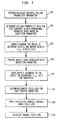
- FIG. 1 a block/flow diagram for a system/method for predicting yield loss in real time is shown.
- killing probability information kp ij is determined.
- killing probability information kp ij is determined as described in a commonly assigned disclosure entitled "SYSTEM AND METHOD FOR DETERMINING YIELD IMPACT FOR SEMICONDUCTOR DEVICES", attorney docket number: 98E9370 US (8706-243), incorporated herein by reference.
- the method to obtain the killing probability kp ij information may alternatively be any method that provides historic killing probability data, as long as the method considers single defects and their characteristics.
- Historic killing probability data may include data on defects and positions thereof on semiconductor wafers previously inspected and tested. Historic killing probability data is maintained to determine trends and/or processing problems in the semiconductor fabrication/inspection process.
- killing probability is determined based on the killing probability information or data of block 102.
- the killing probability is calculated based on historic data and is determined for each subspace in an in-dimensional parameter space. This killing probability is based on two or more inspection tool parameters. For given values of the two or more parameters, subspaces are created corresponding to the values of the parameters. Based on historic killing probability data having the given values, a killing probability is assigned for each subspace.
- an m-dimensional parameter space 200 is illustratively shown where in equals 2.
- Parameter space 200 includes a plurality of subspaces 202.
- Each subspace 202 includes representations of historic data having similar killing probabilities, kp ij .
- kp ij represents killing probabilities in a column i and a row j in parameter space 200.
- a subspace 202a includes a killing probability, kp 11 .
- a subspace 202b includes a killing probability, kp 33 .
- Subspaces 202 are arranged according to parameters in the m-dimensional parameter space. In this example, m equals 2 and the 2 parameters are Grade and Volume.
- Grade is a measure of the intensity of the scattered light at a particular defect
- Volume is a measure of x and y sizes of the defect.
- Other inspections parameters may be used, and these parameters may be different from inspection device to inspection device.
- historic information is organized to provide easy access to specific information in accordance with the present invention.
- a certain number of defects are determined corresponding to these values.
- the defects provide a killing probability as determined in the previously referenced commonly assigned disclosure entitled "SYSTEM AND METHOD FOR DETERMINING YIELD IMPACT FOR SEMICONDUCTOR DEVICES". This killing probability is assigned to a subspace indicated in the 2 parameter space. This is done for each subspace.
- a semiconductor wafer is inspected for defects using an in-line inspection tool.
- This inspection is performed between processing steps (i.e,, in-line) during the fabrication of the semiconductor device.
- In-line inspection tools are known in the art and may include an Orbot WF 730 series, available commercially from Applied Materials, Inc., a Tencor AIT or Tencor 1000 or KLR 2100 series available commercially from KLA-Tencor, Inc.
- the in-line inspection tool generates a result file which displays the results of the inspection as well as specific tool parameters.
- an Orbot WF 736 Duo inspection tool available commercially from Applied Materials, Inc., is employed for inspecting a wafer.
- the inspection tool generates a standard results file, for example, a standard KLA-Tencor results file.
- a partial results file of this type is illustratively shown in FIG. 3.
- a results file 300 is shown in a standard format.
- a parameter list 302 includes defect identification information 304, defect location information 306 and defect characteristic information 308.
- a defect list 312 is also included which has actual data (defect coordinates) and parameter information corresponding to the parameter list 302. Note that the defect parameter information for volume and grade is underlined in the parameter list 302 and the defect list 312.
- an actual defect count is obtained.
- the actual defect count of the semiconductor wafer is comprised of defects with killing probabilities varying between 0 and 1.
- a number of defects for each wafer inspected may be recorded in chart as shown in FIG. 4.
- FIG. 4 a plot or graph 400 of number of defects for each process step of an inspected wafer is shown.
- This graph shows a number of defects (actual defect count) for each inspection process.
- a height of bar 402 gives an overall number of defects for each process step for a given wafer.
- the total number of defects in a given process is illustratively 57 as indicated in FIG. 4.
- Bar 402 may include segments 404. Each segment 404 may represent defects from a set of inspection parameters for a given process step in the semiconductor wafer fabrication process.
- a UCL line is indicated which represents an upper control limit. Wafers with calculated yield loss above this limit are considered out of control and must wait for disposition. Other graphical or tabular representations for the number of defects may also be useful.
- the data of graph 406 will be used as described herein.
- defects from a current wafer which is being considered are ordered in accordance with inspection tool parameters.
- the defects as determined by the inspection tool are illustratively ordered according to grade and volume as shown in FIG. 5.
- the given detects are now associated with the assigned killing probabilities as determined in block 104. Since the present invention classifies defects according to subspaces which are based on inspection parameters, the entire process is capable of automation, i.e., no manual classification is needed since all inspection parameters associated with each individual defect are assigned and recorded using the inspection tools. This saves a significant amount of time.
- a 2-dimensional parameter space 500 is shown having ordered defects according to grade and volume.
- Each subspace 502 has a killing probability associated therewith.
- Each subspace 502 represents a particular killing probability kp ij , and a number of defects n ij are assigned to each subspace 502 according to the inspection parameters.
- the particular killing probability in each subspace 502 is assigned to the defects which are placed according to values of grade and volume (other parameters may be used) in that subspace 502.
- 9 subspaces are illustratively shown more or less subspaces 502 may be used.
- a yield loss is calculated for the current wafer in block 112.
- the yield loss is a defect related yield loss for the process step k.
- kp kij and n kij are determined for each subspace in a parameter space, and entered in EQ. 2 for calculation of yield loss ⁇ Y k for a process step k.
- a block 114 statistical process control is applied to the yield loss ⁇ Y k calculated in block 112.
- the chart includes a more accurate representation of wafer yield than the conventional techniques.
- the disposition of wafers or lots of wafers may be more accurately categorized with respect to the defects determined by in-line inspection tools.
- SPC statistical process control
- a chart or graph 600 is illustratively shown in accordance with the present invention.
- a graph 600 is calculated for each inspection process for a given wafer.
- a bar 602 is generated for each process.
- a height of bar 602 gives an overall predicted yield loss for that process step.
- Yield loss for each subspace may be given by segments 604 of bar 602. Segments 604 accumulate to give the overall yield loss for each process step.
- a graph 606 is generated.
- a UCL line is indicated.
- Other graphical or tabular representations for yield loss may also be useful.
- the present invention provides significant advantages over the prior art. Among these advantages are the capability for automating defect classification in accordance with inspection parameters. All classifying may advantageously be performed without manual inspection or classification.
- the present invention also permits yield loss prediction immediately after in-line inspection thereby providing real time information about the inspected wafers without before electrical testing.
- the present invention has been described in terms of semiconductor in-line process inspection, the present invention is broader and may be applicable to other areas. These other areas may include fabrication processes where multiple systems or parts are inspected and defect data is available. The present invention may then be employed to generate real time yield loss for the products being fabricated.
Landscapes
- Engineering & Computer Science (AREA)
- Quality & Reliability (AREA)
- Computer Vision & Pattern Recognition (AREA)
- Physics & Mathematics (AREA)
- General Physics & Mathematics (AREA)
- Theoretical Computer Science (AREA)
- Testing Or Measuring Of Semiconductors Or The Like (AREA)
- General Factory Administration (AREA)
Applications Claiming Priority (2)
| Application Number | Priority Date | Filing Date | Title |
|---|---|---|---|
| US299979 | 1981-09-08 | ||
| US09/299,979 US6496958B1 (en) | 1999-04-27 | 1999-04-27 | Yield prediction and statistical process control using predicted defect related yield loss |
Publications (2)
| Publication Number | Publication Date |
|---|---|
| EP1049153A2 true EP1049153A2 (fr) | 2000-11-02 |
| EP1049153A3 EP1049153A3 (fr) | 2007-01-03 |
Family
ID=23157144
Family Applications (1)
| Application Number | Title | Priority Date | Filing Date |
|---|---|---|---|
| EP00108734A Withdrawn EP1049153A3 (fr) | 1999-04-27 | 2000-04-22 | Prédiction de rendmeent et processus statistique de contrôle utilisant la prédiction de taux de pertes liés à des défauts |
Country Status (4)
| Country | Link |
|---|---|
| US (1) | US6496958B1 (fr) |
| EP (1) | EP1049153A3 (fr) |
| KR (1) | KR20010014836A (fr) |
| TW (1) | TW587297B (fr) |
Cited By (2)
| Publication number | Priority date | Publication date | Assignee | Title |
|---|---|---|---|---|
| WO2012028705A1 (fr) * | 2010-09-03 | 2012-03-08 | Cascade Microtech Dresden Gmbh | Échantillonneur modulaire et son procédé de fonctionnement |
| CN116466657A (zh) * | 2023-03-17 | 2023-07-21 | 浙江立群汽车配件制造有限公司 | 万向节总成自动化生产加工控制系统 |
Families Citing this family (32)
| Publication number | Priority date | Publication date | Assignee | Title |
|---|---|---|---|---|
| US6701204B1 (en) * | 2000-05-22 | 2004-03-02 | Mosel Vitelic Inc. | System and method for finding defective tools in a semiconductor fabrication facility |
| US6580960B1 (en) * | 2000-06-22 | 2003-06-17 | Promos Technologies, Inc. | System and method for finding an operation/tool combination that causes integrated failure in a semiconductor fabrication facility |
| KR100389135B1 (ko) * | 2001-02-20 | 2003-06-25 | 삼성전자주식회사 | 웨이퍼 디펙트 소스의 성분별 불량칩수 표시 방법 |
| JP4357134B2 (ja) * | 2001-03-29 | 2009-11-04 | 株式会社日立製作所 | 検査システムと検査装置と半導体デバイスの製造方法及び検査プログラム |
| US6681376B1 (en) * | 2001-10-17 | 2004-01-20 | Cypress Semiconductor Corporation | Integrated scheme for semiconductor device verification |
| US7194366B2 (en) * | 2001-10-19 | 2007-03-20 | Auburn University | System and method for estimating reliability of components for testing and quality optimization |
| KR100429883B1 (ko) * | 2001-12-20 | 2004-05-03 | 삼성전자주식회사 | 순수 결함에 의한 불량 발생 확률 측정방법, 순수 결함에서 추출한 패턴 파라미터의 분류를 이용한 결함 제한 수율 측정 방법, 순수 결함에 의한 불량 발생 확률 및 결함 제한 수율을 측정하기 위한 시스템 |
| US6947803B1 (en) * | 2002-09-27 | 2005-09-20 | Advanced Micro Devices, Inc. | Dispatch and/or disposition of material based upon an expected parameter result |
| US7752581B2 (en) * | 2003-06-10 | 2010-07-06 | International Business Machines Corporation | Design structure and system for identification of defects on circuits or other arrayed products |
| US7346470B2 (en) * | 2003-06-10 | 2008-03-18 | International Business Machines Corporation | System for identification of defects on circuits or other arrayed products |
| US6947806B2 (en) * | 2003-09-04 | 2005-09-20 | Promos Technologies Inc. | System and method for effective yield loss analysis for semiconductor wafers |
| US7013441B2 (en) * | 2003-09-26 | 2006-03-14 | International Business Machines Corporation | Method for modeling integrated circuit yield |
| US7849366B1 (en) * | 2004-03-26 | 2010-12-07 | Advanced Micro Devices, Inc. | Method and apparatus for predicting yield parameters based on fault classification |
| US7545531B2 (en) * | 2004-05-18 | 2009-06-09 | Xerox Corporation | Method and apparatus for implementing statistical process control (SPC) in a printing environment |
| US6998867B1 (en) * | 2004-09-01 | 2006-02-14 | International Business Machines Corporation | Enhanced sampling methodology for semiconductor processing |
| US7415378B2 (en) * | 2005-01-31 | 2008-08-19 | Texas Instruments Incorporated | Methods for analyzing critical defects in analog integrated circuits |
| US7496478B2 (en) | 2005-07-18 | 2009-02-24 | Dieter Rathei | Method of monitoring a semiconductor manufacturing trend |
| US20070016321A1 (en) * | 2005-07-18 | 2007-01-18 | Dieter Rathei | Method for screening risk quality semiconductor products |
| KR100679813B1 (ko) * | 2005-12-28 | 2007-02-06 | 동부일렉트로닉스 주식회사 | 반도체 제조에서 잠재적 문제 공정의 통계적 검출 방법 |
| US7485548B2 (en) * | 2006-03-10 | 2009-02-03 | Micron Technology, Inc. | Die loss estimation using universal in-line metric (UILM) |
| JP4333770B2 (ja) * | 2007-04-12 | 2009-09-16 | ソニー株式会社 | マスクパターン作成プログラム、半導体製造方法、マスクパターン作成方法および半導体設計プログラム |
| US8924904B2 (en) * | 2007-05-24 | 2014-12-30 | Applied Materials, Inc. | Method and apparatus for determining factors for design consideration in yield analysis |
| US8799831B2 (en) * | 2007-05-24 | 2014-08-05 | Applied Materials, Inc. | Inline defect analysis for sampling and SPC |
| US7962864B2 (en) * | 2007-05-24 | 2011-06-14 | Applied Materials, Inc. | Stage yield prediction |
| US7937179B2 (en) * | 2007-05-24 | 2011-05-03 | Applied Materials, Inc. | Dynamic inline yield analysis and prediction of a defect limited yield using inline inspection defects |
| US20080319568A1 (en) * | 2007-06-22 | 2008-12-25 | International Business Machines Corporation | Method and system for creating array defect paretos using electrical overlay of bitfail maps, photo limited yield, yield, and auto pattern recognition code data |
| JP2009260176A (ja) * | 2008-04-21 | 2009-11-05 | Nec Electronics Corp | 半導体装置の信頼性予測方法、及びそのプログラム |
| US9129076B2 (en) | 2011-09-05 | 2015-09-08 | United Microelectronics Corp. | Hierarchical wafer yield prediction method and hierarchical lifetime prediction method |
| US10360671B2 (en) * | 2017-07-11 | 2019-07-23 | Kla-Tencor Corporation | Tool health monitoring and matching |
| TWI756784B (zh) * | 2020-08-18 | 2022-03-01 | 國立中央大學 | 用於評估製造系統中的機器良率的裝置及方法 |
| CN115555291B (zh) * | 2022-11-07 | 2023-08-25 | 江苏振宁半导体研究院有限公司 | 一种基于芯片良率的监测装置及方法 |
| CN118655221B (zh) * | 2024-08-09 | 2024-12-13 | 宝鸡市永盛泰钛业有限公司 | 一种基于激光超声的钛合金铸件缺陷检测系统 |
Family Cites Families (4)
| Publication number | Priority date | Publication date | Assignee | Title |
|---|---|---|---|---|
| US3751647A (en) * | 1971-09-22 | 1973-08-07 | Ibm | Semiconductor and integrated circuit device yield modeling |
| US5544256A (en) * | 1993-10-22 | 1996-08-06 | International Business Machines Corporation | Automated defect classification system |
| US5777901A (en) * | 1995-09-29 | 1998-07-07 | Advanced Micro Devices, Inc. | Method and system for automated die yield prediction in semiconductor manufacturing |
| US6265232B1 (en) * | 1998-08-21 | 2001-07-24 | Micron Technology, Inc. | Yield based, in-line defect sampling method |
-
1999
- 1999-04-27 US US09/299,979 patent/US6496958B1/en not_active Expired - Lifetime
-
2000
- 2000-04-22 EP EP00108734A patent/EP1049153A3/fr not_active Withdrawn
- 2000-04-27 KR KR1020000022458A patent/KR20010014836A/ko not_active Abandoned
- 2000-08-08 TW TW089107684A patent/TW587297B/zh not_active IP Right Cessation
Cited By (3)
| Publication number | Priority date | Publication date | Assignee | Title |
|---|---|---|---|---|
| WO2012028705A1 (fr) * | 2010-09-03 | 2012-03-08 | Cascade Microtech Dresden Gmbh | Échantillonneur modulaire et son procédé de fonctionnement |
| CN116466657A (zh) * | 2023-03-17 | 2023-07-21 | 浙江立群汽车配件制造有限公司 | 万向节总成自动化生产加工控制系统 |
| CN116466657B (zh) * | 2023-03-17 | 2023-09-19 | 浙江立群汽车配件制造有限公司 | 万向节总成自动化生产加工控制系统 |
Also Published As
| Publication number | Publication date |
|---|---|
| KR20010014836A (ko) | 2001-02-26 |
| EP1049153A3 (fr) | 2007-01-03 |
| TW587297B (en) | 2004-05-11 |
| US6496958B1 (en) | 2002-12-17 |
Similar Documents
| Publication | Publication Date | Title |
|---|---|---|
| US6496958B1 (en) | Yield prediction and statistical process control using predicted defect related yield loss | |
| JP7216822B2 (ja) | 画素レベル画像定量のための深層学習式欠陥検出及び分類方式の使用 | |
| US6763130B1 (en) | Real time defect source identification | |
| US6334097B1 (en) | Method of determining lethality of defects in circuit pattern inspection method of selecting defects to be reviewed and inspection system of circuit patterns involved with the methods | |
| US7346470B2 (en) | System for identification of defects on circuits or other arrayed products | |
| US5539752A (en) | Method and system for automated analysis of semiconductor defect data | |
| US6408219B2 (en) | FAB yield enhancement system | |
| US6466895B1 (en) | Defect reference system automatic pattern classification | |
| US7113628B1 (en) | Defect image classifying method and apparatus and a semiconductor device manufacturing process based on the method and apparatus | |
| US20140303912A1 (en) | System and method for the automatic determination of critical parametric electrical test parameters for inline yield monitoring | |
| WO2019136190A1 (fr) | Découverte de défauts à l'aide d'une inspection par faisceau d'électrons et d'un apprentissage profond avec une intelligence en temps réel pour réduire les nuisances | |
| US10712289B2 (en) | Inspection for multiple process steps in a single inspection process | |
| US20020032888A1 (en) | System and method for determining yield impact for semiconductor devices | |
| Nurani et al. | In-line defect sampling methodology in yield management: An integrated framework | |
| US6459949B1 (en) | System and method for corrective action tracking in semiconductor processing | |
| US10338004B2 (en) | Production sample shaping that preserves re-normalizability | |
| Shindo et al. | Effective excursion detection by defect type grouping in in-line inspection and classification | |
| Pepper et al. | Inline automated defect classification: a novel approach to defect management | |
| US11295432B2 (en) | Broad band plasma inspection based on a nuisance map | |
| US6769111B2 (en) | Computer-implemented method of process analysis | |
| Munga et al. | A mathematical programming approach for determining control plans in semiconductor manufacturing | |
| Campbell et al. | In-Line Defectivity Methodology for a GaAs Manufacturing Facility | |
| Li et al. | Construction of a" Grand Pareto" for line yield loss, by process loop using limited data sets | |
| Pilon et al. | Intelligent line monitor: maximum productivity through an integrated and automated line monitoring strategy | |
| Proctor | SEMATECH develops software for yield enhancement, defect tracking |
Legal Events
| Date | Code | Title | Description |
|---|---|---|---|
| PUAI | Public reference made under article 153(3) epc to a published international application that has entered the european phase |
Free format text: ORIGINAL CODE: 0009012 |
|
| AK | Designated contracting states |
Kind code of ref document: A2 Designated state(s): AT BE CH CY DE DK ES FI FR GB GR IE IT LI LU MC NL PT SE |
|
| AX | Request for extension of the european patent |
Free format text: AL;LT;LV;MK;RO;SI |
|
| RAP1 | Party data changed (applicant data changed or rights of an application transferred) |
Owner name: INFINEON TECHNOLOGIES RICHMOND, LP |
|
| PUAL | Search report despatched |
Free format text: ORIGINAL CODE: 0009013 |
|
| AK | Designated contracting states |
Kind code of ref document: A3 Designated state(s): AT BE CH CY DE DK ES FI FR GB GR IE IT LI LU MC NL PT SE |
|
| AX | Request for extension of the european patent |
Extension state: AL LT LV MK RO SI |
|
| AKX | Designation fees paid | ||
| STAA | Information on the status of an ep patent application or granted ep patent |
Free format text: STATUS: THE APPLICATION IS DEEMED TO BE WITHDRAWN |
|
| 18D | Application deemed to be withdrawn |
Effective date: 20070704 |
|
| REG | Reference to a national code |
Ref country code: DE Ref legal event code: 8566 |