EP1049257A2 - Phasenauswahlschaltung - Google Patents
Phasenauswahlschaltung Download PDFInfo
- Publication number
- EP1049257A2 EP1049257A2 EP00250086A EP00250086A EP1049257A2 EP 1049257 A2 EP1049257 A2 EP 1049257A2 EP 00250086 A EP00250086 A EP 00250086A EP 00250086 A EP00250086 A EP 00250086A EP 1049257 A2 EP1049257 A2 EP 1049257A2
- Authority
- EP
- European Patent Office
- Prior art keywords
- phase
- tap
- multiplexor
- selection circuit
- circuit
- Prior art date
- Legal status (The legal status is an assumption and is not a legal conclusion. Google has not performed a legal analysis and makes no representation as to the accuracy of the status listed.)
- Granted
Links
Images


Classifications
-
- H—ELECTRICITY
- H03—ELECTRONIC CIRCUITRY
- H03K—PULSE TECHNIQUE
- H03K5/00—Manipulating of pulses not covered by one of the other main groups of this subclass
- H03K5/13—Arrangements having a single output and transforming input signals into pulses delivered at desired time intervals
- H03K5/131—Digitally controlled
Definitions
- This invention relates generally to digital communications, and more specifically to phase selection circuits.
- phase selection circuit For many applications in integrated circuit (IC) design, signal source such as a voltage controlled oscillator (VCO) is utilized to generate a multi-phase clock signal.
- VCO voltage controlled oscillator
- a phase selection circuit is typically utilized in conjunction with signal source to select desired phases.
- Conventional phase selection circuits suffer from various shortcomings, however, including but not limited to, bandwidth, mismatch and/or glitching problems.
- one known phase selection circuit utilizes several stages of multiplexing gates for selecting a desired output phase signal, with each gate being enabled by a select input signal.
- the signals applied to the phase selection circuit must pass through several stages of gates. As the signals pass through each stage of gates, the amount of mismatch caused by the time delay between phases increases. Moreover, the amount of mismatch increases as the number of phases increases.
- Another problem associated with multi-stage phase selection circuits is that the resultant output phase signal is subject to perturbation or glitching when the select input signals for the gates are changed.
- This can be improved somewhat by arranging the select input signals so that the select coding changes from a binary to a Gray code (i.e., a binary code in which sequential numbers are represented by binary expressions each of which differs from the preceding expression by one place only). While utilizing a Gray code helps, perturbation or glitching of the output phase signal remains problematic, particularly when the select inputs for the gates are changed asynchronously.
- phase selection approach utilizes tristateable multiplexors for selecting a desired output phase signal, with each multiplexor enabled by a select input signal. All of the phases applied to a tristateable phase selection circuit are shorted together through tristateable buffers. This approach suffers from various shortcomings, however, including limited bandwidth availability caused by excessive loading of all of the disabled drivers connected to an output node. Additionally, perturbation or glitching at the output phase signal remains problematic.
- the present invention provides, in a first aspect, a phase selection circuit for selecting a phase from a signal source generating phase signals, including a single stage of muitiplexor circuits for receiving phase signals from said signal source, wherein said multiplexor circuits are connected together at their outputs and said phase is shifted by inverting one of said phase signals to said multiplexor circuit.
- the present invention provides a method for selecting a phase, including the steps of generating a plurality of phase signals, receiving the plurality of phase signals using a single stage of multiplexor circuits connected together at their outputs, and inverting one of the plurality of phase signals to the multiplexor circuit to select the phase.
- phase selection circuit 10 for selecting a phase from signal source 12 generating multi-phase signals 14 is illustrated. As described in detail below, phase selection circuit 10 is implemented utilizing a single stage of multiplexor circuits 16 for receiving phase signals 14 associated with delay taps (not shown) from signal source 12. Multiplexor circuits 16, connected together at their outputs 22, select between a tap 18 and an inverse tap 20 and are activated during the entire operation of phase selection circuit 10. The outputs 22 from multiplexor circuits 16 are analog summed together to create a single phase output signal 24 which may be shifted in phase by one tap 18 by inverting one of the input taps to a multiplexor circuit 16, thus reducing perturbation or glitching at output signal 24. Referring to FIG.
- phase interpolation is provided for by further phase shifting the output 22 in steps smaller than one tap 18 utilizing multiplexor circuits 32 which interpolate in multiple steps between tap 18 and inverse tap 20.
- Phase selection circuit 10 provides maximum bandwidth capability, while minimizing mismatch and glitching.
- phase selection circuit 10 provides a one-stage design which leads to good matching characteristics without the reduced bandwidth penalty associated with conventional devices.
- the bandwidth is superior to conventional devices because each multiplexor circuit 16 has an effective fanout of only 1/8 in the present invention, rather than a fanout of one.
- the present invention provides nearly glitch free operation since only one multiplexor circuit 16 is changed at a time, and in addition, even the small amount of glitching that occurs due to the switching of multiplexor circuit 16, is suppressed by the other seven multiplexor circuits 16 which are also driving the output node.
- phase selection circuit 10 includes a single stage of multiplexor circuits 16 for receiving delay taps corresponding to phase signals from signal source 12, such as phase signals ⁇ 00 through ⁇ 15 from VCO (not shown).
- phase selection circuit 10 is described with respect to selecting phases coming off generally equally spaced taps 18 from VCO.
- Signal source 12 is not limited to VCO but rather can be any conventional or newly developed signal source 12 which can generate two or more evenly spaced signals spanning one-half of an oscillation cycle.
- eight 2X1 multiplexor circuits 16 disposed in a single stage are utilized to receive taps 18 from signal source 12.
- the number of multiplexor circuits 16 required to implement phase selection circuit 10 is not limited to eight, but rather is determined in accordance with a number of factors, including but not limited to the number of taps 18 from signal source 12.
- VCO is implemented as an eight-delay stage ring oscillator which produces eight evenly spaced delay output signals which span one-half of a clock period.
- FIG. 4 a phase diagram representing each of the taps 18 from signal source 12 as phases ⁇ 00 through ⁇ 15 , ranging from 0 to 360 degrees, is illustrated.
- the eight additional delay output signals needed to span one complete clock cycle are generated by inverting the first eight delay output signals.
- phase signal ⁇ 08 is equivalent to the inverse of phase signal ⁇ 00
- ⁇ 09 is equivalent to the inverse of phase signal ⁇ 01 and so forth.
- the solid lines 24 represent phase signals 14, ⁇ 00 through ⁇ 07 , respectively, corresponding to each of the delay taps 18, A0 through A7, from signal source.
- the dashed line 26 represents phase signal 14, ⁇ 08 , from delay tap 20, A8, which is generated by inverting delay tap, 18, A0.
- the total phase shift from delay tap 18, A0, to delay tap 18, A7, corresponding to delay phase signals 14, ⁇ 00 through ⁇ 07 is 180 degrees.
- the phase shift between each delay tap 18, such as between delay taps 18, A0 and A1 represents approximately 22.5 degrees.
- a different number of delays could be used or different phase shifts between delays could be established. Implementation of a different number of delays or phase shift between delays would require adjustment of the number of multiplexor circuits 16 required in phase selection circuit 10 shown in FIG. 2.
- all of the multiplexor circuits 16 are connected together at their outputs 22, and all of the multiplexor circuits 16 are always on.
- Phase selection circuit 10 operates by summing and selectively inverting all of the VCO taps 18 in an analog fashion.
- all of the selected phase outputs 22 from multiplexor circuits 16 are summed together in an analog fashion.
- any conventional or newly developed device may be used to sum selected phase outputs 22 together.
- each multiplexor circuit 16 Operation of each multiplexor circuit 16 is controlled by the select signal coupled to SB, which selects the desired input phase. Selection between a tap 18 or inverse tap 20 for each multiplexor circuit 16 can be via a thermometer code or any other conventional or newly developed fashion. Each multiplexor circuit 16 switches its selection from a phase to its complement, or vice versa, when a new value of select signal is applied to SB. Phase of output signal 24 ⁇ out will then follow the average of the eight selected input phases. None of the delay taps 18 from signal source 12 are disabled by phase selection circuit 10 during operation. Rather all of them are summed together in an analog fashion.
- FIGS. 2 and 3(a) for example, the relationship between nine of the sixteen phase signals 14 generated by VCO implemented as a single stage ring oscillator is shown.
- the first multiplexor circuit 16 receives delay tap inputs A0 and A8, the second multiplexor circuit 16 receives delay tap inputs Al and A9, the third multiplexor circuit 16 receives delay tap inputs A2 and A10, the fourth multiplexor circuit 16 receives delay taps A3 and A11, the fifth multiplexor circuit 16 receives delay taps 18 A4 and A12, the sixth multiplexor circuit 16 receives delay taps 18 A5 and A13, the seventh multiplexor circuit 16 receives delay taps 18 A6 and A14 and the eighth multiplexor circuit 16 receives delay taps 18 A7.
- Every multiplexor circuit 16 is left on, i.e. none are ever deactivated, during operation of phase selection circuit 10.
- the selected input phase signals 14 from multiplexor circuits 16 are analog summed together to create a single output phase signal.
- the phase of output phase signal 28 Y1 is equal to the average of the phases of the eight input phase signals 14.
- Adding input phase signals 14 ⁇ 00 through ⁇ 07 in accordance with the present invention will generate an output phase signal 24 having the same phase as the phase signal between phases ⁇ 03 through ⁇ 04 corresponding to a tap value of 3.5.
- phase of output phase signal 28 Y1 To change the phase of output phase signal 28 Y1 from 3.5 to 4.5, only one phase signal out of the entire group of input phase signals 14 needs to be changed from its previous phase. This can be done, for example, by inverting tap 18 A0, which will in effect convert it to tap 20 A8.
- the first multiplexor circuit 16 selects inverse tap 20 A8, rather than tap 18 A0. The remainder of the multiplexor circuits 16 remain activated.
- the phase of the group of taps (A1...A8) will be exactly one tap shifted from the group of taps (A0...A7), and likewise output phase signal 30 Y2 will be shifted in phase by exactly one tap from previous output phase signal 28 Y1.
- phase selection circuit 10 selects a group of continuous phases, in the present example eight phases, out of the ring and adds the selected phases together in an analog fashion to generate a desired output phase signal.
- a different group of eight continuous phases is selected and then analog summed to generate the desired output phase signal 24. Referring to FIG. 4, adjustment of the desired output phase signal 24 results in the group of continuous phases selected being moved around the ring 18.
- phase selection circuit 10 when phase error signal from a phase detector is provided to phase selection circuit 10, a delay tap adjustment is made based on the magnitude and polarity of the phase error signal to reduce the phase error to a nominal amount.
- This dynamic tap adjustment is accomplished when select value signals are provided to phase selection circuit 10. For example, if the initial phase error were to be determined to be 22.5 degrees early, phase selection circuit 10 would be shifted from its previous tap position by inverting one of its tap signals, causing VCO to be shifted in the late direction so that the next phase error from phase detector should be nominal.
- Phase adjustment is accomplished by selectively inverting one of the tap signals from its previous tap position.
- the possible select inputs for SB is shown in TABLE 1 as follows: S7 S6 S5 S4 S3 S2 S1 S0 0 0 0 0 0 0 0 0 0 0 0 0 0 0 0 0 1 1 0 0 0 0 0 0 0 1 1 1 0 0 0
- phase selection circuit serves as a phase interpolator with the ability to output intermediate phases.
- multiplexor circuits 16 in phase selection circuit 10 shown in FIG. 2 are modified to select in fractional amounts how much each of its two inputs 18 and 20 is selected. Fine phase adjustment is performed by shifting the phase of the output signal 24 in steps smaller than one tap. This is accomplished by replacing the 2-to-1 multiplexor circuits 16 which select between a tap 18 and its inverse tap 20, with multiplexor circuits 32 which can, in addition to selecting between a tap 18 and its inverse tap 20, interpolate in multiple steps between a tap 18 and its inverse tap 20.
- phase selection circuit may be comprised of a plurality of multiplexor circuits 32 which, rather than being limited to two-state gates, may be utilized as multiple state gates.
- Multiplexor circuits 32 are preferably implemented in CMOS Current Mode Logic (CML) technology, although other integrated circuit technology may be used as well.
- CML Current Mode Logic
- phase selection circuit 10 is assumed, for illustrative purposes, to have five valid states.
- phase selection circuit 10 is capable of fractionally selecting between the two signals.
- the five available states may be labeled 0, 1, 2, 3 and 4 as follows: SELECT VALUE (STATE) SBN SB ZA 0 1.00 0.00 1.00*A0+0.00*A1 1 0.75 0.25 0.75*A0+0.25*A1 2 0.50 0.50 0.50*A0+0.50*A1 3 0.25 0.75 0.25*A0+0.75*A1 4 0.00 1.00 0.00*A0+1.00*Al
- multiplexor circuit 32 can be modified to provide for a plurality of interpolation states and is not limited to the five states shown in TABLE 2 or discussed herein.
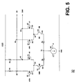
- multiplexor circuit 32 is illustrated in detail.
- Input A0 and its complementary data input A0N are coupled to a pair of differential transistors M2 and M1, respectively.
- AO and A1 are clock signals which are just a little bit delayed from each other.
- the clock signals typically come off a VCO (not shown) so that they are just phases of a clock signal and are very close together so that when the signals are mixed, multiplexor circuit 32 interpolates between them because they are the same signals to start with, with one signal just being a little more delayed than the other so multiplexor circuit 32 can tune between the signals.
- VCO not shown
- input A0 is coupled to the gate 34 of transistor M2 and the complementary data input A0N is coupled to the gate 36 of transistor M1.
- Transistors M1 and M2 have load resistors R1 and R2, respectively.
- the drains 38 and 40 of the M1 and M2 transistors are coupled to the ZA and ZAN outputs, respectively.
- input A1 and its complementary data input A1 N are coupled to a pair of differential transistors M4 and M3, respectively.
- input A1 is coupled to the gate 42 of transistor M4 and the complementary data input A1N is coupled to the gate 44 of transistor M3.
- Transistors M3 and M4 have load resistors R1 and R2, respectively.
- the drains 46 and 48 of the M3 and M4 transistors are coupled to the ZA and ZAN outputs, respectively.
- the drains 38, 40, 46 and 48 of transistors M1, M2, M3 and M4 are also coupled to VDD supply via a load resistor.
- load resistor R1 is coupled to transistors M1 and M3
- load resistor R2 is coupled to transistors M2 and M4.
- the source terminals 50 and 52 of transistors M1 and M2 are coupled at junction 54 so as to share a common current regulated by transistor M5, and the source terminals 56 and 58 of transistors M3 and M4 are coupled at junction 60 so as to share a common current regulated by transistor M6.
- the gates 62 and 64 of transistors M5 and M6 are coupled to differential select inputs SBN and SB, respectively.
- the source terminals 66 and 68 of transistors M5 and M6 are joined at junction 70.
- a constant current source 72 is connected to supply bias current to each transistor M5 and M6.
- the current source 72 is connected to the negative supply rail Vss which may, as shown, be tied to ground, although this is not essential.
- Degeneration resistors Rs may be included to linearize the interpolation function of the multiplexor circuit 32.
- the differential select inputs SB and SBN control the relative amounts of inputs A0 and A1 that contribute to the output signal ZA and ZAN.
- the current is steered entirely or substantially entirely through either transistor M5 or M6.
- the voltages SBN and SB applied to transistors M1 and M2 are 1.00 and 0.00, respectively.
- the voltages SBN and SB applied to transistors M1 and M2 are 0.00 and 1.00, respectively.
- all or substantially all of the current in current source at the bottom flows through transistor M6 because it would be switched fully on and transistor M5 would be switched fully off.
- the muitiplexor circuit instead of being used as a 2-to-1 multiplexor, is used as an interpolator in steering either all or part of the current through transistors M5 or M6.
- part of the total current could be steered through transistor M5, with the remainder steered through transistor M6.
- the fractional voltages SBN and SB applied to transistors M1 and M2 are 0.75 and 0.25, respectively.
- both transistors M5 and M6 would be switched on, with 75% of the current applied to transistor M5 and 25% of the current applied to transistor M6.
- the signal on ZA and ZAN will be a mixture of the two.
- a 64-state selection/interpolation phase selection circuit can be formed as follows: S7 S6 S5 S4 S3 S2 S1 S0 0 0 0 0 0 0 0 0 0 0 0 0 0 0 1 0 0 0 0 0 0 0 2 0 0 0 0 0 0 0 0 3 0 0 0 0 0 0 0 0 4 0 0 0 0 0 0 0 1 4 0 0 0 0 0 0 0 2 4 0 0 0 0 0 0 0 0 3 4 0 0 0 0 0 0 0 0 4 4 0 0 0 0 0 0 1 4 4 0 0 0 0 0 0 0 0 2 4 4 0 0 0 0 0 0 0 0 0 3 4 0 0 0 0 0 0 0 0 4 4
- phase selection circuit 10 The inputs to phase selection circuit 10 are represented by sixteen phases ⁇ 00 through ⁇ 15 which are evenly spaced apart. These sixteen phases represent sixteen coarse adjustment levels across one complete clock cycle. These sixteen phase signals are further subdivided, generating two fine adjustment levels between each coarse adjustment level. Thus, the clock period is divided into 16 X 4 phase divisions.
Landscapes
- Physics & Mathematics (AREA)
- Nonlinear Science (AREA)
- Stabilization Of Oscillater, Synchronisation, Frequency Synthesizers (AREA)
- Manipulation Of Pulses (AREA)
- Stereo-Broadcasting Methods (AREA)
- Circuits Of Receivers In General (AREA)
- Pulse Circuits (AREA)
- Analogue/Digital Conversion (AREA)
Applications Claiming Priority (2)
| Application Number | Priority Date | Filing Date | Title |
|---|---|---|---|
| US265725 | 1999-03-09 | ||
| US09/265,725 US6229344B1 (en) | 1999-03-09 | 1999-03-09 | Phase selection circuit |
Publications (3)
| Publication Number | Publication Date |
|---|---|
| EP1049257A2 true EP1049257A2 (de) | 2000-11-02 |
| EP1049257A3 EP1049257A3 (de) | 2002-01-02 |
| EP1049257B1 EP1049257B1 (de) | 2004-11-03 |
Family
ID=23011645
Family Applications (1)
| Application Number | Title | Priority Date | Filing Date |
|---|---|---|---|
| EP00250086A Expired - Lifetime EP1049257B1 (de) | 1999-03-09 | 2000-03-09 | Phasenauswahlschaltung |
Country Status (6)
| Country | Link |
|---|---|
| US (1) | US6229344B1 (de) |
| EP (1) | EP1049257B1 (de) |
| AT (1) | ATE281710T1 (de) |
| DE (1) | DE60015424T2 (de) |
| DK (1) | DK1049257T3 (de) |
| ES (1) | ES2232380T3 (de) |
Cited By (2)
| Publication number | Priority date | Publication date | Assignee | Title |
|---|---|---|---|---|
| WO2002039585A3 (en) * | 2000-11-13 | 2002-12-05 | Primarion Inc | High bandwidth multi-phase clock selector with continuous phase output |
| EP2779434A1 (de) * | 2013-03-15 | 2014-09-17 | Analog Devices, Inc. | Vorrichtung und Verfahren zur umkehrbarer zur Sinusformung zur Phaseninterpolation |
Families Citing this family (7)
| Publication number | Priority date | Publication date | Assignee | Title |
|---|---|---|---|---|
| US6233294B1 (en) * | 1999-08-17 | 2001-05-15 | Richard Bowers | Method and apparatus for accomplishing high bandwidth serial communication between semiconductor devices |
| US20030210758A1 (en) * | 2002-04-30 | 2003-11-13 | Realtek Semiconductor Corp. | Recovered clock generator with high phase resolution and recovered clock generating method |
| KR100486276B1 (ko) * | 2002-11-05 | 2005-04-29 | 삼성전자주식회사 | 입력되는 두 클럭의 인터폴레이팅에 의하여 지연량의차이를 조절할 수 있는 지연된 탭신호들을 발생하는 회로 |
| EP1473828A1 (de) * | 2003-04-30 | 2004-11-03 | STMicroelectronics S.r.l. | Phasendetektor und dazugehöriges Verfahren zum Erzeugen eines die Phasenverschiebung darstellenden Signals |
| US8155018B2 (en) * | 2004-03-03 | 2012-04-10 | Qualcomm Atheros, Inc. | Implementing location awareness in WLAN devices |
| US7046072B2 (en) * | 2004-03-03 | 2006-05-16 | Atheros Communications, Inc. | Commutating phase selector |
| US8957704B1 (en) * | 2013-09-06 | 2015-02-17 | Synopsys, Inc. | High speed phase selector with a glitchless output used in phase locked loop applications |
Family Cites Families (11)
| Publication number | Priority date | Publication date | Assignee | Title |
|---|---|---|---|---|
| US5034967A (en) * | 1988-11-14 | 1991-07-23 | Datapoint Corporation | Metastable-free digital synchronizer with low phase error |
| US5485490A (en) * | 1992-05-28 | 1996-01-16 | Rambus, Inc. | Method and circuitry for clock synchronization |
| US5355035A (en) * | 1993-01-08 | 1994-10-11 | Vora Madhukar B | High speed BICMOS switches and multiplexers |
| US5561692A (en) * | 1993-12-09 | 1996-10-01 | Northern Telecom Limited | Clock phase shifting method and apparatus |
| US5475344A (en) * | 1994-02-22 | 1995-12-12 | The Board Of Trustees Of The Leland Stanford Junior University | Multiple interconnected ring oscillator circuit |
| US5570294A (en) * | 1994-03-11 | 1996-10-29 | Advanced Micro Devices | Circuit configuration employing a compare unit for testing variably controlled delay units |
| US5552745A (en) * | 1994-09-21 | 1996-09-03 | International Business Machines Corporation | Self-resetting CMOS multiplexer with static output driver |
| US5644604A (en) * | 1994-11-14 | 1997-07-01 | Hal Computer Systems, Inc. | Digital phase selector system and method |
| JPH08321827A (ja) * | 1995-03-20 | 1996-12-03 | Fujitsu Ltd | データ識別装置及びこれを用いた光受信器 |
| EP0783797B1 (de) * | 1995-07-21 | 2003-11-05 | Koninklijke Philips Electronics N.V. | Vorrichtung zur drahtlosen digitalen kommunikation und pulsformungsnetzwerk |
| US6034570A (en) * | 1997-06-27 | 2000-03-07 | Vitesse Semiconductor Corporation | Gallium arsenide voltage-controlled oscillator and oscillator delay cell |
-
1999
- 1999-03-09 US US09/265,725 patent/US6229344B1/en not_active Expired - Lifetime
-
2000
- 2000-03-09 DK DK00250086T patent/DK1049257T3/da active
- 2000-03-09 AT AT00250086T patent/ATE281710T1/de not_active IP Right Cessation
- 2000-03-09 EP EP00250086A patent/EP1049257B1/de not_active Expired - Lifetime
- 2000-03-09 ES ES00250086T patent/ES2232380T3/es not_active Expired - Lifetime
- 2000-03-09 DE DE60015424T patent/DE60015424T2/de not_active Expired - Fee Related
Cited By (3)
| Publication number | Priority date | Publication date | Assignee | Title |
|---|---|---|---|---|
| WO2002039585A3 (en) * | 2000-11-13 | 2002-12-05 | Primarion Inc | High bandwidth multi-phase clock selector with continuous phase output |
| US6621312B2 (en) | 2000-11-13 | 2003-09-16 | Primarion, Inc. | High bandwidth multi-phase clock selector with continuous phase output |
| EP2779434A1 (de) * | 2013-03-15 | 2014-09-17 | Analog Devices, Inc. | Vorrichtung und Verfahren zur umkehrbarer zur Sinusformung zur Phaseninterpolation |
Also Published As
| Publication number | Publication date |
|---|---|
| DE60015424D1 (de) | 2004-12-09 |
| EP1049257B1 (de) | 2004-11-03 |
| ES2232380T3 (es) | 2005-06-01 |
| EP1049257A3 (de) | 2002-01-02 |
| ATE281710T1 (de) | 2004-11-15 |
| DE60015424T2 (de) | 2005-10-27 |
| DK1049257T3 (da) | 2005-03-14 |
| US6229344B1 (en) | 2001-05-08 |
Similar Documents
| Publication | Publication Date | Title |
|---|---|---|
| EP1538753B1 (de) | Phasenkombinationsschaltung und Taktsignalgenerator zur Signalübertragung mit hoher Geschwindigkeit | |
| US7443219B2 (en) | Phase interpolation apparatus, systems, and methods | |
| JP4049511B2 (ja) | 位相合成回路およびタイミング信号発生回路 | |
| US7928789B2 (en) | Methods and apparatus for improved phase switching and linearity in an analog phase interpolator | |
| JP2002353781A (ja) | 内部クロック発生回路 | |
| US20030006817A1 (en) | Digital phase interpolator for controlling delay time and method thereof | |
| EP1049257B1 (de) | Phasenauswahlschaltung | |
| KR101038470B1 (ko) | 동작영역이 넓은 디지털제어발진기 | |
| US6310568B1 (en) | Digital-to-analog conversion circuit | |
| US6751745B1 (en) | Digital synchronization circuit provided with circuit for generating polyphase clock signal | |
| US6377102B2 (en) | Load equalization in digital delay interpolators | |
| US20070075757A1 (en) | Voltage controlled delay line (VCDL) having embedded multiplexer and interpolation functions | |
| KR101271750B1 (ko) | 임베디드 멀티플렉서 기능과 보간 기능을 갖는 전압 제어지연 라인 | |
| US20070096784A1 (en) | Delay locked loop circuit | |
| Garlepp et al. | A portable digital DLL architecture for CMOS interface circuits | |
| US6940331B2 (en) | Delayed tap signal generating circuit for controlling delay by interpolating two input clocks | |
| US6472944B2 (en) | Voltage controlled oscillator with delay circuits | |
| JP4238931B2 (ja) | 発振回路 | |
| JP2003115761A (ja) | D/aコンバータ | |
| JP2011082639A (ja) | 半導体集積回路 | |
| JP2006060874A (ja) | 発振回路 |
Legal Events
| Date | Code | Title | Description |
|---|---|---|---|
| PUAI | Public reference made under article 153(3) epc to a published international application that has entered the european phase |
Free format text: ORIGINAL CODE: 0009012 |
|
| AK | Designated contracting states |
Kind code of ref document: A2 Designated state(s): AT BE CH CY DE DK ES FI FR GB GR IE IT LI LU MC NL PT SE |
|
| AX | Request for extension of the european patent |
Free format text: AL;LT;LV;MK;RO;SI |
|
| PUAL | Search report despatched |
Free format text: ORIGINAL CODE: 0009013 |
|
| AK | Designated contracting states |
Kind code of ref document: A3 Designated state(s): AT BE CH CY DE DK ES FI FR GB GR IE IT LI LU MC NL PT SE |
|
| AX | Request for extension of the european patent |
Free format text: AL;LT;LV;MK;RO;SI |
|
| 17P | Request for examination filed |
Effective date: 20020702 |
|
| AKX | Designation fees paid |
Free format text: AT BE CH CY DE DK ES FI FR GB GR IE IT LI LU MC NL PT SE |
|
| GRAP | Despatch of communication of intention to grant a patent |
Free format text: ORIGINAL CODE: EPIDOSNIGR1 |
|
| GRAS | Grant fee paid |
Free format text: ORIGINAL CODE: EPIDOSNIGR3 |
|
| GRAA | (expected) grant |
Free format text: ORIGINAL CODE: 0009210 |
|
| AK | Designated contracting states |
Kind code of ref document: B1 Designated state(s): AT BE CH CY DE DK ES FI FR GB GR IE IT LI LU MC NL PT SE |
|
| REG | Reference to a national code |
Ref country code: GB Ref legal event code: FG4D |
|
| REG | Reference to a national code |
Ref country code: CH Ref legal event code: EP |
|
| REF | Corresponds to: |
Ref document number: 60015424 Country of ref document: DE Date of ref document: 20041209 Kind code of ref document: P |
|
| REG | Reference to a national code |
Ref country code: IE Ref legal event code: FG4D |
|
| PGFP | Annual fee paid to national office [announced via postgrant information from national office to epo] |
Ref country code: DE Payment date: 20050105 Year of fee payment: 6 |
|
| PG25 | Lapsed in a contracting state [announced via postgrant information from national office to epo] |
Ref country code: GR Free format text: LAPSE BECAUSE OF FAILURE TO SUBMIT A TRANSLATION OF THE DESCRIPTION OR TO PAY THE FEE WITHIN THE PRESCRIBED TIME-LIMIT Effective date: 20050203 |
|
| PGFP | Annual fee paid to national office [announced via postgrant information from national office to epo] |
Ref country code: AT Payment date: 20050218 Year of fee payment: 6 |
|
| REG | Reference to a national code |
Ref country code: SE Ref legal event code: TRGR |
|
| PGFP | Annual fee paid to national office [announced via postgrant information from national office to epo] |
Ref country code: GB Payment date: 20050223 Year of fee payment: 6 |
|
| REG | Reference to a national code |
Ref country code: CH Ref legal event code: NV Representative=s name: E. BLUM & CO. PATENTANWAELTE |
|
| PG25 | Lapsed in a contracting state [announced via postgrant information from national office to epo] |
Ref country code: IE Free format text: LAPSE BECAUSE OF NON-PAYMENT OF DUE FEES Effective date: 20050309 Ref country code: FI Free format text: LAPSE BECAUSE OF NON-PAYMENT OF DUE FEES Effective date: 20050309 Ref country code: CY Free format text: LAPSE BECAUSE OF FAILURE TO SUBMIT A TRANSLATION OF THE DESCRIPTION OR TO PAY THE FEE WITHIN THE PRESCRIBED TIME-LIMIT Effective date: 20050309 |
|
| REG | Reference to a national code |
Ref country code: DK Ref legal event code: T3 |
|
| PGFP | Annual fee paid to national office [announced via postgrant information from national office to epo] |
Ref country code: NL Payment date: 20050317 Year of fee payment: 6 |
|
| PGFP | Annual fee paid to national office [announced via postgrant information from national office to epo] |
Ref country code: FR Payment date: 20050318 Year of fee payment: 6 |
|
| PGFP | Annual fee paid to national office [announced via postgrant information from national office to epo] |
Ref country code: BE Payment date: 20050322 Year of fee payment: 6 |
|
| PGFP | Annual fee paid to national office [announced via postgrant information from national office to epo] |
Ref country code: SE Payment date: 20050323 Year of fee payment: 6 Ref country code: DK Payment date: 20050323 Year of fee payment: 6 Ref country code: CH Payment date: 20050323 Year of fee payment: 6 |
|
| PGFP | Annual fee paid to national office [announced via postgrant information from national office to epo] |
Ref country code: LU Payment date: 20050325 Year of fee payment: 6 |
|
| PG25 | Lapsed in a contracting state [announced via postgrant information from national office to epo] |
Ref country code: MC Free format text: LAPSE BECAUSE OF NON-PAYMENT OF DUE FEES Effective date: 20050331 |
|
| PGFP | Annual fee paid to national office [announced via postgrant information from national office to epo] |
Ref country code: ES Payment date: 20050413 Year of fee payment: 6 |
|
| REG | Reference to a national code |
Ref country code: ES Ref legal event code: FG2A Ref document number: 2232380 Country of ref document: ES Kind code of ref document: T3 |
|
| PLBE | No opposition filed within time limit |
Free format text: ORIGINAL CODE: 0009261 |
|
| STAA | Information on the status of an ep patent application or granted ep patent |
Free format text: STATUS: NO OPPOSITION FILED WITHIN TIME LIMIT |
|
| ET | Fr: translation filed | ||
| 26N | No opposition filed |
Effective date: 20050804 |
|
| REG | Reference to a national code |
Ref country code: IE Ref legal event code: MM4A |
|
| PG25 | Lapsed in a contracting state [announced via postgrant information from national office to epo] |
Ref country code: GB Free format text: LAPSE BECAUSE OF NON-PAYMENT OF DUE FEES Effective date: 20060309 Ref country code: AT Free format text: LAPSE BECAUSE OF NON-PAYMENT OF DUE FEES Effective date: 20060309 |
|
| PG25 | Lapsed in a contracting state [announced via postgrant information from national office to epo] |
Ref country code: SE Free format text: LAPSE BECAUSE OF NON-PAYMENT OF DUE FEES Effective date: 20060310 Ref country code: ES Free format text: LAPSE BECAUSE OF NON-PAYMENT OF DUE FEES Effective date: 20060310 |
|
| PG25 | Lapsed in a contracting state [announced via postgrant information from national office to epo] |
Ref country code: LU Free format text: LAPSE BECAUSE OF NON-PAYMENT OF DUE FEES Effective date: 20060331 Ref country code: LI Free format text: LAPSE BECAUSE OF NON-PAYMENT OF DUE FEES Effective date: 20060331 Ref country code: DK Free format text: LAPSE BECAUSE OF NON-PAYMENT OF DUE FEES Effective date: 20060331 Ref country code: CH Free format text: LAPSE BECAUSE OF NON-PAYMENT OF DUE FEES Effective date: 20060331 Ref country code: BE Free format text: LAPSE BECAUSE OF NON-PAYMENT OF DUE FEES Effective date: 20060331 |
|
| PGFP | Annual fee paid to national office [announced via postgrant information from national office to epo] |
Ref country code: IT Payment date: 20060331 Year of fee payment: 7 |
|
| PG25 | Lapsed in a contracting state [announced via postgrant information from national office to epo] |
Ref country code: NL Free format text: LAPSE BECAUSE OF NON-PAYMENT OF DUE FEES Effective date: 20061001 |
|
| PG25 | Lapsed in a contracting state [announced via postgrant information from national office to epo] |
Ref country code: DE Free format text: LAPSE BECAUSE OF NON-PAYMENT OF DUE FEES Effective date: 20061003 |
|
| REG | Reference to a national code |
Ref country code: DK Ref legal event code: EBP |
|
| REG | Reference to a national code |
Ref country code: CH Ref legal event code: PL |
|
| EUG | Se: european patent has lapsed | ||
| GBPC | Gb: european patent ceased through non-payment of renewal fee |
Effective date: 20060309 |
|
| NLV4 | Nl: lapsed or anulled due to non-payment of the annual fee |
Effective date: 20061001 |
|
| REG | Reference to a national code |
Ref country code: FR Ref legal event code: ST Effective date: 20061130 |
|
| REG | Reference to a national code |
Ref country code: ES Ref legal event code: FD2A Effective date: 20060310 |
|
| BERE | Be: lapsed |
Owner name: *VITESSE SEMICONDUCTOR CORP. Effective date: 20060331 |
|
| PG25 | Lapsed in a contracting state [announced via postgrant information from national office to epo] |
Ref country code: PT Free format text: LAPSE BECAUSE OF NON-PAYMENT OF DUE FEES Effective date: 20050403 |
|
| PG25 | Lapsed in a contracting state [announced via postgrant information from national office to epo] |
Ref country code: FR Free format text: LAPSE BECAUSE OF NON-PAYMENT OF DUE FEES Effective date: 20060331 |
|
| PG25 | Lapsed in a contracting state [announced via postgrant information from national office to epo] |
Ref country code: IT Free format text: LAPSE BECAUSE OF NON-PAYMENT OF DUE FEES Effective date: 20070309 |