EP1050106B1 - Limitation de courant inverse d'un transistor mos - Google Patents
Limitation de courant inverse d'un transistor mos Download PDFInfo
- Publication number
- EP1050106B1 EP1050106B1 EP98964306A EP98964306A EP1050106B1 EP 1050106 B1 EP1050106 B1 EP 1050106B1 EP 98964306 A EP98964306 A EP 98964306A EP 98964306 A EP98964306 A EP 98964306A EP 1050106 B1 EP1050106 B1 EP 1050106B1
- Authority
- EP
- European Patent Office
- Prior art keywords
- transistor
- voltage
- output
- coupled
- circuit
- Prior art date
- Legal status (The legal status is an assumption and is not a legal conclusion. Google has not performed a legal analysis and makes no representation as to the accuracy of the status listed.)
- Expired - Lifetime
Links
- 238000013459 approach Methods 0.000 claims description 15
- 239000004065 semiconductor Substances 0.000 claims description 8
- 229910044991 metal oxide Inorganic materials 0.000 claims description 7
- 150000004706 metal oxides Chemical class 0.000 claims description 7
- 238000000034 method Methods 0.000 claims description 4
- 238000001514 detection method Methods 0.000 description 9
- 230000001419 dependent effect Effects 0.000 description 4
- 230000008859 change Effects 0.000 description 2
- 238000005259 measurement Methods 0.000 description 2
- 230000008569 process Effects 0.000 description 2
- 230000000750 progressive effect Effects 0.000 description 2
- 230000000630 rising effect Effects 0.000 description 2
- 230000002146 bilateral effect Effects 0.000 description 1
- 230000000295 complement effect Effects 0.000 description 1
- 238000010276 construction Methods 0.000 description 1
- 238000013461 design Methods 0.000 description 1
- 230000001066 destructive effect Effects 0.000 description 1
- 230000000694 effects Effects 0.000 description 1
- 239000000463 material Substances 0.000 description 1
- 238000012986 modification Methods 0.000 description 1
- 230000004048 modification Effects 0.000 description 1
- 238000012544 monitoring process Methods 0.000 description 1
- 230000004044 response Effects 0.000 description 1
- 238000011896 sensitive detection Methods 0.000 description 1
- 239000000758 substrate Substances 0.000 description 1
Images


Classifications
-
- H—ELECTRICITY
- H03—ELECTRONIC CIRCUITRY
- H03K—PULSE TECHNIQUE
- H03K19/00—Logic circuits, i.e. having at least two inputs acting on one output; Inverting circuits
- H03K19/003—Modifications for increasing the reliability for protection
-
- H—ELECTRICITY
- H03—ELECTRONIC CIRCUITRY
- H03K—PULSE TECHNIQUE
- H03K19/00—Logic circuits, i.e. having at least two inputs acting on one output; Inverting circuits
- H03K19/003—Modifications for increasing the reliability for protection
- H03K19/00346—Modifications for eliminating interference or parasitic voltages or currents
- H03K19/00361—Modifications for eliminating interference or parasitic voltages or currents in field effect transistor circuits
-
- H—ELECTRICITY
- H03—ELECTRONIC CIRCUITRY
- H03K—PULSE TECHNIQUE
- H03K19/00—Logic circuits, i.e. having at least two inputs acting on one output; Inverting circuits
- H03K19/003—Modifications for increasing the reliability for protection
- H03K19/00315—Modifications for increasing the reliability for protection in field-effect transistor circuits
Definitions
- the present invention relates generally to interface circuits, and specifically, to a circuit for allowing full forward current and throttling reverse current in an output stage MOS transistor.
- a metal oxide semiconductor (“MOS”) transistor is a bilateral device. When the MOS transistor is on, current may flow in either direction depending on the ON resistance and the differential voltage across the device. In specific applications, such as a CMOS driver connected to a multi-party line, it is desirable for current to flow freely in one direction, and to be greatly restricted in the opposing direction. In a transmitter driver application for a three volt interface circuit, there are the combined requirements for high forward drive currents (e.g., greater than 10 mA) at a low Vds (e.g., 0.2 Volts) and a very low (or zero) reverse current.
- high forward drive currents e.g., greater than 10 mA
- Vds e.g., 0.2 Volts
- Forward current is defined as a positive current flowing from the positive supply (VCC) through the MOS device to the output or from the output through the MOS device into the negative supply (VEE or GND). Except for the forward voltage drop across a diode (Vbe), the diode (p-n junction) exhibits the required circuit function.
- An active rectification circuit can provide the required function but there are accuracy and hysteresis problems in determining when the MOS transistor should and should not conduct.
- the MOS transistor in the transmitter driver application where the driver is attached to a multi-party line, the MOS transistor must be able to protect against the potential for reverse current which may be caused by an external circuit pulling the output beyond the supply rails, by noise, or by ringing due to improper line termination. If the MOS transistor turns off at an output voltage beyond the supply rail, significant reverse current may flow, depending on the MOS transistor ON resistance, until the turn off voltage is reached.
- the reverse current may result in back-charging the supply, which can be destructive to a non-rechargeable battery.
- the MOS device must also behave properly when nothing external is driving the output, and there is only an external load with resistance ranging from a short circuit up to and including an open circuit. If the MOS transistor turns completely off prior to the output reaching the supply rail voltage, an external load can cause the output to droop. It will continue to droop due to the external load until the MOS device again turns on. The difference in the output voltage from turn off to turn on is the hysteresis of the active rectification circuit. When the MOS transistor is turned off prior to the output reaching the supply voltage, the output will "chatter", oscillating between turn off and turn on voltages.
- FIG. 1 illustrates a prior art output interface circuit.
- four series connected MOS transistors MP1, MP2, MN2 and MN1 are shown.
- MP1 and MN1 remain fully-on, and MP2 and MN2 are switched in such a way that MP2 or MN2 is on to drive VOUT high or low, respectively, but both are never on together.
- the addition of MP1 and MN1 to the elementary switching circuit provides a means for active rectification.
- the incentive for the addition of MP1 and MN1 in lieu of diodes is to eliminate the forward Vbe of the diodes.
- the forward Vbe is typically greater than 0.8 Volts at temperature. This voltage is replaced by the Vds (drain-to-source voltage) of a MOS device, which is a size/strength dependent variable, but typically sized to never exceed 0.3 Volts.
- Figure 2 illustrates a cross section of the prior art output interface circuit.
- Figure 2 shows a P-well process with isolated pockets on a p-type substrate.
- the output interface circuit may equally be built in an n-well process.
- PMOS devices MP1 and MP2 are isolated in a local n- pocket 10.
- the potential of the n- pocket 10 is that of Node P1 and is maintained by the voltage on the common sources 14 and 16 of MP1 and MP2, when either or both of MP1 and MP2 are on, in parallel with the p+(12)/n-(10) diode DP1 and the P+(18)/n-(10) diode DP2.
- NMOS devices MN1 and MN2 are isolated in a second local n- pocket 20. The potential of this pocket is held at VCC.
- p- P-well
- the potential of the P-well 30 is that of the Node W1 and is maintained by the voltage on the common sources 26 and 24 of MN1 and MN2, when either or both of these devices are on, in parallel with the p-(30)/n+(28) body diode DN1 and the p-(30)/n+(22) body diode DN2.
- voltage sensitive detection circuitry is constantly monitoring VOUT relative to VCC and GND.
- gate GP1 is connected to Node P1 which turns off MP1.
- a small current flows from VOUT through MP2, if ON, or through DP2 if MP2 is OFF, which will charge up Node P1 to the VOUT voltage level. Once charged up to VOUT, no more current will flow.
- a complementary action takes place on the NMOS side of the circuit when VOUT is determined to be at or below GND.
- gate GN1 is connected to Node W1. This turns off MN1.
- a small current flows from W1 through MN2, if ON, or through DN2 if MN2 is OFF, to discharge W1 to the VOUT voltage level.
- the invention is a means for ensuring full current flow in the "forward" direction in a MOS transistor, and substantially reducing (and/or eliminating) current flow in the "reverse” direction.
- the forward voltage drop and reverse current are controllable and are determined by ratios of device size.
- the present invention is a circuit coupled to an output stage transistor having an output voltage thereon to ensure current flow in one direction and to throttle current flow in a reverse direction.
- the circuit includes a first circuit coupled to the output transistor to progressively turn off the same as the output voltage reaches a first threshold voltage and approaches a rail voltage.
- the circuit further includes a second circuit coupled to the output transistor to turn off the same as the output voltage reaches a second threshold voltage where the second threshold voltage is greater than the rail voltage.
- the MOS transistor when operating in the positive current mode with the driver output voltage well below the supply voltage, the MOS transistor is fully-on.
- the driver output voltage is at a first threshold near the supply voltage
- the MOS transistor begins to progressively turn off such that the electrical resistance of the device increases in inverse proportion to the driver output voltage from the supply rail.
- the resistance of the MOS transistor is at its maximum finite value (off being equivalent to infinite resistance).
- the MOS transistor turns off completely ("fully-off").
- the present invention solves the problem of supply back drive by making the resistance of the MOS device, while in the resistive condition, a design parameter. While the MOS transistor is in the positive current mode, the invention solves the problem of threshold voltage accuracy in the active rectifier by the use of progressive turn off and high ON resistance in the reverse current mode prior to the turn off threshold voltage.
- the invention solves the problem of driver output droop and "chatter" for any load because in the progressive turn off mode the MOS device resistance varies to compensate the load at a finite driver output voltage. If the driver output is open (infinite load resistance), the driver output voltage is equal to the supply voltage. The MOS device resistance does not become infinite (fully-off) until the driver output voltage exceeds the supply voltage.
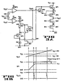
- Figure 3A illustrates a PMOS detection and control circuitry of the present invention while Figure 3B illustrates various signals of the circuitry in Figure 3A.
- the detection and control circuitry is coupled to the driver circuit of Figure 1 (consisting of devices MP1, MP2, MN1, and MN2) and controls the PMOS side.
- comparator C1 and amplifier A1 both sense VOUT.
- Voltage reference VCC-VS1 is coupled to the inverting terminal of A1
- voltage reference VCC+VS2 is coupled to the non-inverting terminal of C1.
- IS1 is a voltage-controlled current source and IS2 is a fixed current source.
- the current level of IS1 ranges from 0 to N time IS2 (where N is greater than 1).
- Both IS1 and IS2 are non-ideal current sources in that positive current will be sourced only when there is a voltage drop across the current source, otherwise the current will be less, but not less than zero.
- Vds or Vtp i.e., the PMOS threshold
- VOUT When VOUT is in the region between VCC-VS1 and VCC (between points A & C in Figure 3B), the current source IS1 conducts linearly as VOUT approaches VCC. Devices MP3 and MP5 remain OFF while devices MN7 and MP6 remain ON. As the current level of IS1 approaches and exceeds that of IS2, the gate voltage GP1 of MP1 rises rapidly. As the voltage on Node GP1 rises, it will approach the PMOS gate threshold which begins to turn OFF MP1, limiting the current to pull VOUT up. If there is nothing external pulling up on VOUT, a stable point is reached where VOUT ceases to rise and the gate voltage GP1 is held steady. If there is no external load (to GND) on VOUT, then VOUT will be pulled to VCC.
- VOUT will settle to a voltage near VCC where the current through the load is balanced by the current through MP1. If there is an external driver pulling VOUT above VCC, reverse current will begin to flow although restricted by the near-threshold gate drive of MP1.
- the body diode of MP6 is reverse biased when GP1 is greater than VCC, thus preventing reverse current through MP6 when OFF.
- the voltage on Node GP1 follows the voltage on Node P1, which in turn follows VOUT, and the only remaining current flow is through IS2 to GND.
- MP4 With the gate-to-drain connection, MP4 is at the edge of saturation, with a Vds equal to the PMOS threshold (Vtp), at the IS2 current level.
- MP1 has a very low Vds with nearly the same gate-to-source (Vgs) voltage as MP4, and is in the triode region.
- Vgs gate-to-source
- the source of MP4 is in series with IS1 and MP6 to VCC. Both have a small but non zero voltage drop which subtracts from the effective Vgs of MP4. As VOUT and the voltage on Node P1 rise above VCC, this adds to the effective Vgs of MP1. Additionally, there are differing body-effects offsetting the thresholds of each MOS device.
- the net result is that while the ability to mirror MP1 is not perfect it is adequate as a means for creating operating limits to the MP1 reverse current.
- the maximum reverse current may be set.
- the voltage sources VS1 and VS2 equate to built-in offsets in A1 and C1, respectively, and provide a means for adjusting the functional switch points. These switch points provide a buffer region about the reverse bias point, and eliminate the need for precision in voltage or current detection.
- VOUT has hysteresis such that the reference for a rising input is above VCC and for a falling input is below VCC.
- VOUT falls (between points D & B in Figure 3B)
- the circuit does not change states and MP1 remains off until VOUT and the voltage on Node P1 are less than VCC, but greater than VCC-VS1.
- COUT1 goes high and the voltage on Node GP1 drops to its linear range to turn on MP1 with restricted current flow.
- Device MP5 turns OFF and devices MN7 and MP6 turn ON.
- VOUT approaches VCC-VS1
- the voltage on Node GP1 continues to drop, and once it passes below VCC-VS1, the voltage on Node GP1 is at GND and MP1 is "fully-on".
- Figure 4A illustrates a NMOS detection and control circuitry of the present invention while Figure 4B illustrates various signals of the circuitry in Figure 4A.
- VOUT is coupled to the inverting terminals of the comparator C2 and Amplifier A2.
- Voltage references GND+VS3 and GND-VS4 are coupled to the non-inverting terminals of A2 and C2, respectively.
- IS4 is a voltage-controlled current source while IS3 is a fixed current source.
- the current level of IS4 ranges from 0 to N time IS3 (where N is greater than 1).
- Both IS3 and IS4 are non-ideal current sources in that positive current will be sourced only when there is a voltage drop.across the current source, otherwise the current will be less, but not less than zero.
- Vds or Vtp i.e., the NMOS threshold
- the current source IS4 conducts linearly as VOUT approaches GND.
- Devices MN3 and MN5 remain OFF while devices MP7 and MN6 remain ON.
- the gate voltage GN1 of MN1 falls rapidly.
- the voltage on Node GN1 falls, it will approach the NMOS gate threshold which begins to turn OFF MN1, limiting the current to pull VOUT down. If there is nothing external pulling down on VOUT, a stable point is reached where VOUT ceases to fall and the gate voltage GN1 is held steady.
- VOUT If there is no external load (to VCC) on VOUT, then VOUT will be pulled to GND. If there is a load, VOUT will settle to a voltage near GND where the current through the load is balanced by the current through MN1. If there is an external driver pulling VOUT below GND, reverse current will begin to flow although restricted by the near-threshold gate drive of MN1.
- Devices MN4, MN5, and MN6 are co-located in an isolated P-well in the same manner as MN1 and MN2 (referring to Figures 1 and 2).
- the body diode of MN6 is reverse biased when GN1 is less than GND, thus preventing reverse current through MN6 when OFF.
- the voltage on Node GN1 follows the voltage on Node W1, which in turn follows VOUT, and the only remaining current flow is through IS3 from VCC.
- VOUT is now traversed from a voltage level below GND-VS4 to a voltage level greater than GND+VS3, assuming MN2 is ON.
- the comparator C2 has hysteresis such that the reference for a falling input is below GND and for a rising input is above GND.
- VOUT rises (between points D & B in Figure 3B)
- the circuit does not change states and MN1 remains off until VOUT and the voltage on Node W1 are greater than GND, but less than GND+VS3.
- VOUT rises above the C2 threshold to the left of point B
- COUT2 goes low and the voltage on Node GN1 rises to its linear range to turn on MN1 with restricted current flow.
- Device MN5 turns OFF and devices MP7 and MN6 turn ON.
- VOUT approaches GND+VS3
- the voltage on Node GN1 continues to drop, and once it passes above GND+VS3, the voltage on Node GN1 is at VCC and MN1 is "fully-on".
Landscapes
- Physics & Mathematics (AREA)
- Engineering & Computer Science (AREA)
- Computer Hardware Design (AREA)
- Computing Systems (AREA)
- General Engineering & Computer Science (AREA)
- Mathematical Physics (AREA)
- Electronic Switches (AREA)
- Logic Circuits (AREA)
Claims (31)
- Circuit couplé à un transistor de sortie d'un premier type de conductivité (MP1) comprenant une grille, un drain couplé à une borne d'alimentation en énergie ayant une tension de rail sur celle-ci, et une source couplée à une borne de sortie ayant une tension de sortie sur celle-ci, le circuit étant destiné à garantir une circulation de courant dans une direction et à étrangler une circulation de courant dans une direction inverse, comprenant :un premier circuit (A1, MP4, MP5, MP6) couplé à la grille du transistor de sortie pour commuter progressivement à l'état bloqué le transistor de sortie lorsque la tension de sortie (Vout) atteint une première tension de seuil et approche la tension de rail ; etun deuxième circuit (C1, MP3) couplé à la grille et à la source du transistor de sortie pour commuter à l'état bloqué le transistor de sortie lorsque la tension de sortie (Vout) atteint une deuxième tension de seuil, la deuxième tension de seuil étant supérieure à la tension de rail.
- Circuit selon la revendication 1, dans lequel le transistor de sortie est un transistor semi-conducteur à oxyde métallique à canal P.
- Circuit selon la revendication 1, dans lequel le premier circuit (A1, MP4-MP6) commute progressivement à l'état bloqué le transistor de sortie (MP1) de manière que la résistance électrique du transistor de sortie augmente en proportion inverse de la différence entre la tension de sortie (Vout) et la tension de rail (Vcc) lorsque la tension de sortie approche la tension de rail.
- Circuit selon la revendication 1, dans lequel le premier circuit comprend :dans lequel quand la tension de sortie (Vout) augmente entre la tension de rail (Vcc) et la deuxième tension de seuil, et un courant maximum dans la direction inverse est fonction de la dimension du transistor et du niveau de courant de la source de courant.un transistor (MP1) du premier type de conductivité ayant une grille, une source couplée à la borne d'alimentation en énergie et un drain, la grille et le drain étant couplés à la grille du transistor de sortie ; etune source de courant (IS1) couplée au drain du transistor ;
- Circuit selon la revendication 1, dans lequel le premier circuit comprend :un amplificateur (A1) ayant une borne de non inversion avec la tension de sortie appliquée à celle-ci et une borne d'inversion avec la première tension de seuil appliquée à celle-ci ;une source de courant commandée en tension (IS1) couplée à une sortie de l'amplificateur (A1) et à la borne d'alimentation en énergie, ayant la tension de rail (Vcc) sur celle-ci ; etun transistor relié à une diode et couplé à la source de courant commandée en tension (IS1).
- Circuit selon la revendication 5, dans lequel le transistor relié à une diode comprend :un transistor du premier type de conductivité (MP4) ayant une grille, une source couplée à la source de courant commandée en tension et un drain couplé aux grilles du transistor et du transistor de sortie ; etune deuxième source de courant (IS2) ayant une première borne couplée au drain du transistor et à la grille du transistor de sortie et une deuxième borne couplée à une deuxième borne d'alimentation en énergie (GND).
- Circuit selon la revendication 6, dans lequel la source de courant commandée en tension (IS1) a un niveau de courant allant de 0 à N fois le niveau de courant de la deuxième source de courant, où N est supérieur à un.
- Circuit selon la revendication 1, dans lequel le premier circuit comprend :un amplificateur (A1) ayant une borne de non inversion avec la tension de sortie appliquée à celle-ci et une borne d'inversion avec la première tension de seuil appliquée à celle-ci ;une source de courant commandée en tension (IS1) couplée à une sortie de l'amplificateur (A1) et à la borne d'alimentation en énergie (Vcc) ;un transistor (MP4) du premier type de conductivité ayant une grille, une source couplée à la source de courant commandée en tension et un drain couplé aux grilles du transistor et du transistor de sortie ; etune deuxième source de courant (IS1) ayant une première borne couplée au drain du transistor et à la grille du transistor de sortie et une deuxième borne couplée à une deuxième borne d'alimentation en énergie (Vcc).
- Circuit selon la revendication 1, dans lequel le deuxième circuit comprend :un comparateur (C1) ayant une borne de non inversion avec la deuxième tension de seuil (VS2) appliquée à celle-ci et une borne d'inversion avec la tension de sortie (Vout) appliquée à celle-ci ; etun transistor (MP3) couplé au comparateur et au transistor de sortie, ledit transistor étant destiné à commuter à l'état bloqué le transistor de sortie (MP1) quand la tension de sortie (Vout) est sensiblement la même que la deuxième tension de seuil.
- Circuit selon la revendication 1, dans lequel le deuxième circuit comprend :un comparateur (C1) ayant une borne de non inversion avec la deuxième tension de seuil (VS2) appliquée à celle-ci et une home d'inversion avec la tension de sortie (Vout) appliquée à celle-ci ; etun transistor (MP3) du premier type de conductivité ayant une grille, un drain et une source, la grille étant couplée à une sortie du comparateur et le drain et la source étant couplés à la grille et à la source du transistor de sortie, respectivement, ledit transistor couple la grille et la source du transistor de sortie (MP1) pour commuter celles-ci à l'état bloqué quand la tension de sortie est sensiblement la même que la deuxième tension de seuil (VS2).
- Circuit selon la revendication 8, dans lequel le deuxième circuit comprend :un comparateur (C1) ayant une borne de non inversion avec la deuxième tension de seuil (VS2) appliquée à celle-ci et une borne d'inversion avec la tension de sortie (Vout) appliquée à celle-ci ; etun deuxième transistor (MP3) couplé au comparateur et au transistor de sortie, ledit deuxième transistor étant destiné à commuter à l'état bloqué le transistor de sortie (MP1) quand la tension de sortie (Vout) est sensiblement la même que la deuxième tension de seuil.
- Circuit selon la revendication 11, comprenant en outre un troisième circuit couplé aux premier et deuxième circuits pour valider le premier circuit quand la tension de sortie est inférieure à la deuxième tension de seuil (VS2).
- Circuit selon la revendication 12, dans lequel le troisième circuit comprend :un troisième transistor du premier type de conductivité ayant une grille, un drain couplé à la source de courant commandée en tension et une source couplée à la source du premier transistor ;un quatrième transistor du premier type de conductivité ayant une grille couplée à la sortie du comparateur (C1), un drain couplé à la grille du troisième transistor et une source couplée à la source du premier transistor ; etun cinquième transistor (MN7) d'un deuxième type de conductivité ayant une grille couplée à la grille du quatrième transistor, un drain couplé à la grille du troisième transistor et une source couplée à la deuxième borne d'alimentation en énergie (GND).
- Circuit selon la revendication 13, dans lequel quand la tension de sortie est sensiblement égale ou supérieure à la deuxième tension de seuil, le troisième transistor se commute à l'état bloqué pour bloquer une circulation de courant inverse à travers la source de courant commandée en tension (IS1) et vers la tension de rail.
- Circuit selon la revendication 13, dans lequel des transistors du premier type de conductivité (MP1-MP6) sont des transistors semi-conducteurs à oxyde métallique à canal P et des transistors du deuxième type de conductivité sont des transistors semi-conducteurs à oxyde métallique à canal N.
- Circuit couplé à un transistor de sortie d'un premier type de conductivité (MP1) comprenant une grille, un drain couplé à une borne d'alimentation en énergie ayant une tension de rail (Vcc) sur celle-ci, et une source couplée à une borne de sortie ayant une tension de sortie sur celle-ci, le circuit étant destiné à garantir une circulation de courant dans une direction et pour étrangler une circulation de courant dans une direction inverse, comprenant :un premier circuit (A2, IS3, IS4, MN4-6, MP7) couplé à la grille du transistor de sortie pour commuter progressivement à l'état bloqué le transistor de sortie lorsque la tension de sortie atteint une première tension de seuil et approche la tension de rail ; etun deuxième circuit (C2 ;MN3) couplé à la grille et à la source du transistor de sortie pour commuter à l'état bloqué le transistor de sortie lorsque la tension de sortie (Vout) atteint une deuxième tension de seuil, la deuxième tension de seuil étant inférieure à la tension de rail.
- Circuit selon la revendication 16, dans lequel le transistor de sortie est un transistor semi-conducteur à oxyde métallique à canal N.
- Circuit selon la revendication 16, dans lequel le premier circuit commute progressivement à l'état bloqué le transistor de sortie (MN1) de manière que la résistance électrique du transistor de sortie augmente en proportion inverse de la différence entre la tension de sortie (Vout) et la tension de rail lorsque la tension de sortie approche la tension de rail (GND).
- Circuit selon la revendication 16, dans lequel le premier circuit comprend :dans lequel quand la tension de sortie diminue entre la tension de rail et la deuxième tension de seuil (VS4), un courant maximum dans la direction inverse est fonction de la tailledu transistor et du niveau de courant de la source de courant.un transistor (MN3) du premier type de conductivité ayant une grille, une source couplée à la borne d'alimentation en énergie et un drain, la grille et le drain étant couplés à la grille du transistor de sortie (MN1) ; etune source de courant (IS3) couplée au drain du transistor ;
- Circuit selon la revendication 16, dans lequel le premier circuit comprend :un amplificateur (A2) ayant une borne de non inversion avec la première tension de seuil (VS3) appliquée à celle-ci et une borne d'inversion avec la tension de sortie appliquée à celle-ci ;une source de courant commandée en tension (154) couplée à une sortie de l'amplificateur et à la borne d'alimentation en énergie ; etun transistor relié à une diode et couplé à la source de courant commandée en tension.
- Circuit selon la revendication 20, dans lequel le transistor relié à une diode comprend :un transistor du premier type de conductivité ayant une grille, une source couplée à la source de courant commandée en tension (IS4) et un drain couplé aux grilles du transistor et du transistor de sortie (MN1) ; etune deuxième source de courant (IS3) ayant une première borne couplée au drain du transistor et à la grille du transistor de sortie et une deuxième borne couplée à une deuxième borne d'alimentation en énergie (Vcc).
- Circuit selon la revendication 21, dans lequel la source de courant commandée en tension (IS4) a un niveau de courant allant de 0 à N fois le niveau de courant de la deuxième source de courant où N est supérieur à un.
- Circuit selon la revendication 16, dans lequel le premier circuit comprend :un amplificateur (A2) ayant une borne de non inversion avec la première tension de seuil (VS3) appliquée à celle-ci et une borne d'inversion avec la tension de sortie appliquée à celle-ci ;une source de courant commandée en tension (IS4) couplée à une sortie de l'amplificateur et à la borne d'alimentation en énergie ;un transistor du premier type de conductivité ayant une grille, une source couplée à la source de courant commandée en tension et un drain couplé aux grilles du transistor et du transistor de sortie ; etune deuxième source de courant (IS3) ayant une première borne couplée au drain du transistor et à la grille du transistor de sonic (MN1) et une deuxième borne couplée à une deuxième borne d'alimentation en énergie.
- Circuit selon la revendication 16, dans lequel le deuxième circuit comprend :un comparateur (C2) ayant une borne de non inversion avec la deuxième tension de seuil (VS4) appliquée à celle-ci et une borne d'inversion avec la tension de sortie appliquée à celle-ci ; etun transistor (MN3) couplé au comparateur et au transistor de sortie, ledit transistor étant destiné à commuter à l'état bloqué le transistor de sortie quand la tension de sortie est sensiblement la même que la deuxième tension de seuil.
- Circuit selon la revendication 16, dans lequel le deuxième circuit comprend :un comparateur (C1) ayant une borne de non inversion avec la deuxième tension de seuil appliquée à celle-ci et une borne d'inversion avec la tension de sortie appliquée à celle-ci ; etun transistor (MN3) du premier type de conductivité ayant une grille, un drain et une source, la grille étant couplée à une sortie du comparateur et le drain et la source étant couplés à la grille et à la source du transistor de sortie (MN1), respectivement, et ledit transistor couple la grille et la source du transistor de sortie pour commuter à l'état bloqué le transistor de sortie quand la tension de sortie (Vout) est sensiblement la même que la deuxième tension de seuil.
- Circuit selon la revendication 23, dans lequel le deuxième circuit comprend :un comparateur (C1) ayant une borne de non inversion avec la deuxième tension de seuil appliquée à celle-ci et une borne d'inversion avec la tension de sortie appliquée à celle-ci ; etun deuxième transistor (MN3) couplé au comparateur et au transistor de sortie, ledit transistor étant destiné à commuter à l'état bloqué le transistor de sortie quand la tension de sortie (Vout) est sensiblement la même que la deuxième tension de seuil (VS4).
- Circuit selon la revendication 26, comprenant en outre un troisième circuit couplé aux premier et deuxième circuits pour valider le premier circuit quand la tension de sortie (Vout) est supérieure à la deuxième tension de seuil.
- Circuit selon la revendication 27, dans lequel le troisième circuit comprend :un troisième transistor du premier type de conductivité ayant une gille, un drain couplé à la source de courant commandée en tension (IS4) et une source couplée à la source du premier transistor ;un quatrième transistor du premier type de conductivité ayant une grille couplée à la sortie du comparateur, un drain couplé à la grille du troisième transistor et une source couplée à la source du premier transistor ; etun cinquième transistor d'un deuxième type de conductivité (MP7) ayant une grille couplée à la grille du quatrième transistor, un drain couplé à la grille du troisième transistor et une source couplée à la deuxième borne d'alimentation en énergie.
- Circuit selon la revendication 28, dans lequel quand la tension de sortie est sensiblement égale ou inférieure à la deuxième tension de seuil et le troisième transistor se commute à l'état bloqué pour bloquer une circulation de courant inverse provenant de la tension de rail et à travers la source de courant commandée en tension.
- Circuit selon la revendication 28, dans lequel des transistors du premier type de conductivité sont des transistors semi-conducteurs à oxyde métallique à canal N et des transistors du deuxième type de conductivité sont des transistors semi-conducteurs à oxyde métallique à canal P.
- Procédé pour garantir une circulation de courant dans une direction et étrangler une circulation de courant dans une direction inverse dans un transistor de sortie comprenant une grille, un drain couplé à une borne d'alimentation en énergie ayant une tension de rail sur celle-ci, et une source couplée à une borne de sortie ayant une tension de sortie sur celle-ci, comprenant les étapes consistant à :commuter à l'état bloqué le transistor de sortie progressivement lorsque la tension de sortie atteint la première tension de seuil et approche la tension de rail de manière qu'une résistance électrique du transistor de sortie augmente en proportion inverse de la différence entre la tension de sortie et la tension de rail lorsque la tension de sortie approche la tension de rail ; etcommuter à l'état bloqué le transistor de sortie lorsque la tension de sortie atteint une deuxième tension de seuil, la tension de rail étant une tension entre la première tension de seuil et la deuxième tension de seuil.
Applications Claiming Priority (3)
| Application Number | Priority Date | Filing Date | Title |
|---|---|---|---|
| US12516 | 1998-01-23 | ||
| US09/012,516 US5963067A (en) | 1998-01-23 | 1998-01-23 | Reverse current throttling of a MOS transistor |
| PCT/US1998/027635 WO1999038259A1 (fr) | 1998-01-23 | 1998-12-28 | Limitation de courant inverse d'un transistor mos |
Publications (2)
| Publication Number | Publication Date |
|---|---|
| EP1050106A1 EP1050106A1 (fr) | 2000-11-08 |
| EP1050106B1 true EP1050106B1 (fr) | 2005-09-14 |
Family
ID=21755326
Family Applications (1)
| Application Number | Title | Priority Date | Filing Date |
|---|---|---|---|
| EP98964306A Expired - Lifetime EP1050106B1 (fr) | 1998-01-23 | 1998-12-28 | Limitation de courant inverse d'un transistor mos |
Country Status (7)
| Country | Link |
|---|---|
| US (1) | US5963067A (fr) |
| EP (1) | EP1050106B1 (fr) |
| JP (1) | JP2002502140A (fr) |
| KR (1) | KR20010034331A (fr) |
| DE (1) | DE69831604D1 (fr) |
| TW (1) | TW404043B (fr) |
| WO (1) | WO1999038259A1 (fr) |
Families Citing this family (5)
| Publication number | Priority date | Publication date | Assignee | Title |
|---|---|---|---|---|
| US6137339A (en) * | 1997-08-28 | 2000-10-24 | Lucent Technologies Inc. | High voltage integrated CMOS driver circuit |
| US6621300B1 (en) * | 2002-04-23 | 2003-09-16 | Silicon Graphics, Inc. | System and method for improving speed of operation of integrated circuits |
| US7737784B2 (en) * | 2008-10-09 | 2010-06-15 | Maxim Integrated Products, Inc. | Self configuring output stages of precision amplifiers |
| KR102073746B1 (ko) * | 2018-08-13 | 2020-02-05 | 세메스 주식회사 | 기판 온도 제어 장치, 그를 포함하는 기판 처리 장치 및 기판 처리 방법 |
| CN110635795B (zh) * | 2019-10-22 | 2022-11-22 | 上海南芯半导体科技股份有限公司 | 适用于中高压工作的高电源电压选择电路及其实现方法 |
Family Cites Families (5)
| Publication number | Priority date | Publication date | Assignee | Title |
|---|---|---|---|---|
| DE4334513C1 (de) * | 1993-10-09 | 1994-10-20 | Itt Ind Gmbh Deutsche | CMOS-Schaltung mit erhöhter Spannungsfestigkeit |
| US5455732A (en) * | 1993-09-15 | 1995-10-03 | National Semiconductor Corporation | Buffer protection against output-node voltage excursions |
| US5414314A (en) * | 1994-06-09 | 1995-05-09 | Maxim Integrated Products | High swing interface stage |
| FR2724072A1 (fr) * | 1994-08-25 | 1996-03-01 | Philips Composants | Etage amplificateur de puissance, de type suiveur. |
| JP2806324B2 (ja) * | 1995-08-25 | 1998-09-30 | 日本電気株式会社 | 内部降圧回路 |
-
1998
- 1998-01-23 US US09/012,516 patent/US5963067A/en not_active Expired - Lifetime
- 1998-12-28 JP JP2000529037A patent/JP2002502140A/ja active Pending
- 1998-12-28 WO PCT/US1998/027635 patent/WO1999038259A1/fr not_active Ceased
- 1998-12-28 DE DE69831604T patent/DE69831604D1/de not_active Expired - Lifetime
- 1998-12-28 EP EP98964306A patent/EP1050106B1/fr not_active Expired - Lifetime
- 1998-12-28 KR KR1020007008058A patent/KR20010034331A/ko not_active Withdrawn
-
1999
- 1999-01-22 TW TW088100999A patent/TW404043B/zh not_active IP Right Cessation
Also Published As
| Publication number | Publication date |
|---|---|
| DE69831604D1 (de) | 2005-10-20 |
| WO1999038259A1 (fr) | 1999-07-29 |
| JP2002502140A (ja) | 2002-01-22 |
| US5963067A (en) | 1999-10-05 |
| TW404043B (en) | 2000-09-01 |
| KR20010034331A (ko) | 2001-04-25 |
| EP1050106A1 (fr) | 2000-11-08 |
Similar Documents
| Publication | Publication Date | Title |
|---|---|---|
| EP0372956B1 (fr) | Circuit de source de courant constante | |
| US7969191B2 (en) | Low-swing CMOS input circuit | |
| US5939933A (en) | Intentionally mismatched mirror process inverse current source | |
| US10454466B1 (en) | Biasing cascode transistors of an output buffer circuit for operation over a wide range of supply voltages | |
| JP7144960B2 (ja) | 電源電圧監視回路 | |
| US5668483A (en) | CMOS buffer having stable threshold voltage | |
| US7248079B2 (en) | Differential buffer circuit with reduced output common mode variation | |
| US7388410B2 (en) | Input circuits configured to operate using a range of supply voltages | |
| JP6871514B2 (ja) | 負電源制御回路及び電源装置 | |
| EP0880735B1 (fr) | Miroir de courant cmos | |
| JPS636918A (ja) | Cmos−入力回路 | |
| US10498333B1 (en) | Adaptive gate buffer for a power stage | |
| WO1983000785A1 (fr) | Circuit comparateur cmos a haute vitesse | |
| US11881859B2 (en) | Schmitt trigger circuit having mismatched input and supply | |
| US6759878B2 (en) | Voltage comparator circuit and substrate bias adjusting circuit using same | |
| CN101924541B (zh) | 用于自适应跳闸点检测的设备和方法 | |
| JPH05327455A (ja) | 中間電位発生回路 | |
| EP1050106B1 (fr) | Limitation de courant inverse d'un transistor mos | |
| CN109643137B (zh) | 低压参考电流电路 | |
| US11489519B2 (en) | Analog switch with boost current for fast turn on | |
| US7218169B2 (en) | Reference compensation circuit | |
| US5710516A (en) | Input logic signal buffer circuits | |
| US20220337158A1 (en) | Voltage conversion circuit having self-adaptive mechanism | |
| US6362666B1 (en) | Precision and fast recovery buffer | |
| US20150236683A1 (en) | High voltage comparison circuit |
Legal Events
| Date | Code | Title | Description |
|---|---|---|---|
| PUAI | Public reference made under article 153(3) epc to a published international application that has entered the european phase |
Free format text: ORIGINAL CODE: 0009012 |
|
| 17P | Request for examination filed |
Effective date: 20000816 |
|
| AK | Designated contracting states |
Kind code of ref document: A1 Designated state(s): DE FR GB IE IT NL |
|
| GRAP | Despatch of communication of intention to grant a patent |
Free format text: ORIGINAL CODE: EPIDOSNIGR1 |
|
| GRAS | Grant fee paid |
Free format text: ORIGINAL CODE: EPIDOSNIGR3 |
|
| GRAA | (expected) grant |
Free format text: ORIGINAL CODE: 0009210 |
|
| AK | Designated contracting states |
Kind code of ref document: B1 Designated state(s): DE FR GB IE IT NL |
|
| PG25 | Lapsed in a contracting state [announced via postgrant information from national office to epo] |
Ref country code: NL Free format text: LAPSE BECAUSE OF FAILURE TO SUBMIT A TRANSLATION OF THE DESCRIPTION OR TO PAY THE FEE WITHIN THE PRESCRIBED TIME-LIMIT Effective date: 20050914 Ref country code: IT Free format text: LAPSE BECAUSE OF FAILURE TO SUBMIT A TRANSLATION OF THE DESCRIPTION OR TO PAY THE FEE WITHIN THE PRE;WARNING: LAPSES OF ITALIAN PATENTS WITH EFFECTIVE DATE BEFORE 2007 MAY HAVE OCCURRED AT ANY TIME BEFORE 2007. THE CORRECT EFFECTIVE DATE MAY BE DIFFERENT FROM THE ONE RECORDED.SCRIBED TIME-LIMIT Effective date: 20050914 |
|
| REG | Reference to a national code |
Ref country code: GB Ref legal event code: FG4D |
|
| REG | Reference to a national code |
Ref country code: IE Ref legal event code: FG4D |
|
| REF | Corresponds to: |
Ref document number: 69831604 Country of ref document: DE Date of ref document: 20051020 Kind code of ref document: P |
|
| PG25 | Lapsed in a contracting state [announced via postgrant information from national office to epo] |
Ref country code: DE Free format text: LAPSE BECAUSE OF FAILURE TO SUBMIT A TRANSLATION OF THE DESCRIPTION OR TO PAY THE FEE WITHIN THE PRESCRIBED TIME-LIMIT Effective date: 20051215 |
|
| PG25 | Lapsed in a contracting state [announced via postgrant information from national office to epo] |
Ref country code: GB Free format text: LAPSE BECAUSE OF NON-PAYMENT OF DUE FEES Effective date: 20051228 |
|
| PG25 | Lapsed in a contracting state [announced via postgrant information from national office to epo] |
Ref country code: IE Free format text: LAPSE BECAUSE OF NON-PAYMENT OF DUE FEES Effective date: 20051229 |
|
| NLV1 | Nl: lapsed or annulled due to failure to fulfill the requirements of art. 29p and 29m of the patents act | ||
| PLBE | No opposition filed within time limit |
Free format text: ORIGINAL CODE: 0009261 |
|
| STAA | Information on the status of an ep patent application or granted ep patent |
Free format text: STATUS: NO OPPOSITION FILED WITHIN TIME LIMIT |
|
| 26N | No opposition filed |
Effective date: 20060615 |
|
| GBPC | Gb: european patent ceased through non-payment of renewal fee |
Effective date: 20051228 |
|
| REG | Reference to a national code |
Ref country code: IE Ref legal event code: MM4A |
|
| PG25 | Lapsed in a contracting state [announced via postgrant information from national office to epo] |
Ref country code: FR Free format text: LAPSE BECAUSE OF FAILURE TO SUBMIT A TRANSLATION OF THE DESCRIPTION OR TO PAY THE FEE WITHIN THE PRESCRIBED TIME-LIMIT Effective date: 20061020 |
|
| EN | Fr: translation not filed | ||
| EN | Fr: translation not filed | ||
| PG25 | Lapsed in a contracting state [announced via postgrant information from national office to epo] |
Ref country code: FR Free format text: LAPSE BECAUSE OF FAILURE TO SUBMIT A TRANSLATION OF THE DESCRIPTION OR TO PAY THE FEE WITHIN THE PRESCRIBED TIME-LIMIT Effective date: 20051231 |
|
| PG25 | Lapsed in a contracting state [announced via postgrant information from national office to epo] |
Ref country code: FR Free format text: LAPSE BECAUSE OF FAILURE TO SUBMIT A TRANSLATION OF THE DESCRIPTION OR TO PAY THE FEE WITHIN THE PRESCRIBED TIME-LIMIT Effective date: 20050914 |