EP1050137B1 - Leitungstreiber mit linearen übergängen - Google Patents
Leitungstreiber mit linearen übergängen Download PDFInfo
- Publication number
- EP1050137B1 EP1050137B1 EP99900846A EP99900846A EP1050137B1 EP 1050137 B1 EP1050137 B1 EP 1050137B1 EP 99900846 A EP99900846 A EP 99900846A EP 99900846 A EP99900846 A EP 99900846A EP 1050137 B1 EP1050137 B1 EP 1050137B1
- Authority
- EP
- European Patent Office
- Prior art keywords
- delay
- coupled
- switching
- output
- cable driver
- Prior art date
- Legal status (The legal status is an assumption and is not a legal conclusion. Google has not performed a legal analysis and makes no representation as to the accuracy of the status listed.)
- Expired - Lifetime
Links
- 230000005540 biological transmission Effects 0.000 claims abstract description 17
- 230000001276 controlling effect Effects 0.000 claims 1
- 230000001105 regulatory effect Effects 0.000 claims 1
- 208000032365 Electromagnetic interference Diseases 0.000 abstract 1
- 230000007704 transition Effects 0.000 description 28
- 239000003990 capacitor Substances 0.000 description 17
- 230000001965 increasing effect Effects 0.000 description 8
- 230000005670 electromagnetic radiation Effects 0.000 description 7
- 230000003111 delayed effect Effects 0.000 description 5
- 230000000694 effects Effects 0.000 description 3
- 238000000034 method Methods 0.000 description 3
- 238000007493 shaping process Methods 0.000 description 2
- 239000002131 composite material Substances 0.000 description 1
- 230000001419 dependent effect Effects 0.000 description 1
- 238000010586 diagram Methods 0.000 description 1
- 238000005516 engineering process Methods 0.000 description 1
- 230000001939 inductive effect Effects 0.000 description 1
- 238000009434 installation Methods 0.000 description 1
- 230000003071 parasitic effect Effects 0.000 description 1
Images


Classifications
-
- H—ELECTRICITY
- H04—ELECTRIC COMMUNICATION TECHNIQUE
- H04L—TRANSMISSION OF DIGITAL INFORMATION, e.g. TELEGRAPHIC COMMUNICATION
- H04L25/00—Baseband systems
- H04L25/02—Details ; arrangements for supplying electrical power along data transmission lines
- H04L25/0264—Arrangements for coupling to transmission lines
- H04L25/028—Arrangements specific to the transmitter end
-
- H—ELECTRICITY
- H04—ELECTRIC COMMUNICATION TECHNIQUE
- H04L—TRANSMISSION OF DIGITAL INFORMATION, e.g. TELEGRAPHIC COMMUNICATION
- H04L25/00—Baseband systems
- H04L25/02—Details ; arrangements for supplying electrical power along data transmission lines
- H04L25/03—Shaping networks in transmitter or receiver, e.g. adaptive shaping networks
- H04L25/03828—Arrangements for spectral shaping; Arrangements for providing signals with specified spectral properties
- H04L25/03834—Arrangements for spectral shaping; Arrangements for providing signals with specified spectral properties using pulse shaping
-
- H—ELECTRICITY
- H04—ELECTRIC COMMUNICATION TECHNIQUE
- H04L—TRANSMISSION OF DIGITAL INFORMATION, e.g. TELEGRAPHIC COMMUNICATION
- H04L25/00—Baseband systems
- H04L25/02—Details ; arrangements for supplying electrical power along data transmission lines
- H04L25/0264—Arrangements for coupling to transmission lines
- H04L25/0272—Arrangements for coupling to multiple lines, e.g. for differential transmission
Definitions
- This invention relates to the field of data communications. More particularly, the invention relates to cable drivers, line drivers, wave shaping of digital pulses and rise and fall control circuits.
- the transmission of digital data along a transmission line may be accomplished using a cable driver.
- the cable driver receives the signal to be transmitted and generates a corresponding signal on the transmission line.
- One objective in the design of cable drivers is to maximize the rate at which data may be transmitted (the "data rate") on the transmission line.
- the maximum data rate which may be transmitted will be limited by two considerations:
- Prior art cable drivers control the rise and fall times of the output signal with a resistor-capacitor circuit. Such circuits exhibit exponential low to high and high to low output transitions with the result that the output signal takes a relatively long time to settle within the specified tolerance to minimize jitter, while still having a sufficiently long rise and fall time. Consequently, the data rate which can be transmitted by prior art cable drivers is limited.
- European patent application 607,677 discloses an integrated wave shaping circuit. This circuit produces an output waveform by generating a number of step signals. The magnitude of the step signals and their relative timing is selected to produce an output wave form which approximates the desired output waveform.
- the output waveform itself is non linear. This patent application does not recognize the problems set out above: avoidance of electromagnetic radiation by providing a generally linear output waveform over a selected portion of the output signal and reducing jitter in the output waveform.
- European patent application 763,917 discloses a line driver for use with data lines requiring intermediate voltage levels between a high and a low level. These lines include 10baseT and 100baseT ethernet systems. This circuit also produces a series of step signals separated by a selected delay period. The step signals are combined to produce an output signal which may have one of four output voltage levels. The output waveform of this device is also non-linear, as required by the 10baseT and 100baseT specifications described in the Background section of EP763,917.
- the maximum data rate which can be transmitted may be increased by designing the cable driver to have linear low to high and high to low output transitions.
- the primary feature of the improved cable driver is the ability to transmit data at higher data rates without increased jitter or electromagnetic radiation.
- the improved cable driver reduced the problems of ringing and overshoot in the output signal.
- a cable driver comprising an (a) an input port for receiving an input signal, comprising first and second input terminals; (b) an output port for transmitting an output signal on a transmission line, comprising first and second output terminals; (c) a first resistance and a second resistance for defining said output signal at said output port, said first resistance being coupled between a voltage source and said first output terminal and said second resistance being coupled between said voltage source and said second output terminal; (d) a plurality of switching stages, wherein each of said switching stages comprises a switch and a current source associated with said switch for producing a current, said current source being coupled to its associated switch for controlling the switching time of said associated switch and each of said switches being coupled to said output port, said plurality of switching stages including a first switching stage; (e) a plurality of delay stages for providing a delay time, (f) said first switching stage being coupled to said input port and the remaining switching stages being coupled in series, wherein one of said delay stages is coupled between each successive pair of said switching stages, such
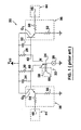
- FIG. 1 shows a prior art cable driver 20 for transmitting a digital signal over a transmission line.
- the prior art cable driver 20 comprises an input port 22, a switch 24, a current source 26, resistors 28 and 30, capacitors 32 and 34, output stages 36 and 38 and an output port 44.
- Capacitor 32 and resistor 28 are connected in parallel between V CC and node 42.
- Capacitor 34 and resistor 30 are connected in parallel between V CC and node 40.
- Current source 26 is coupled between switch 24 and ground.
- Switch 24 is responsive to an input received at input port 22 and may couple current source 26 to node 42 through node H or to node 40 through node L.
- Output port 44 comprises output terminals 46 and 48.
- Output stage 36 comprises transistor Q 1 and resistors 50 and 52.
- Transistor Q 1 is connected as an emitter follower stage.
- the base of transistor Q 1 is connected to node 42.
- the emitter of transistor Q 1 is coupled to ground through resistor 52 and to output terminal 46 through resistor 50.
- the collector of transistor Q 1 is coupled to V CC .
- Output stage 38 is similarly comprised of a transistor Q 2 and two resistors 54 and 56.
- the base of transistor Q 2 is connected to node 40.
- the emitter of transistor Q 2 is coupled to ground through resistor 56 and to output terminal 48 through resistor 54.
- the collector of transistor Q 2 is connected to V CC .
- the prior art cable driver 20 will be configured to produce a differential output signal V out at output terminals 46 and 48.
- the differential output signal V out will be positive when V 48 is higher than V 46 and this condition will be referred to as a high output signal.
- the differential output signal V out will be negative when V 48 is lower than V 46 and this condition will be referred to as a low output signal.
- the prior art cable driver 20 operates as follows.
- a differential input signal, V in is received at input port 22, which comprises input terminals 58 and 60, and is directed to switch 24.
- the differential input signal consists of two voltage signals, one of which is received at terminal 58 and the other of which is received at terminal 60.
- V in V IL
- Switch 24 is responsive to the differential input signal V in and switches between nodes L and H depending on whether differential input signal V in is low or high, respectively. When differential input signal V in is high, switch 24 will connect current source 26 to node H and conversely, when differential input signal V in is low, switch 24 will connect current source 26 to node L.
- switch 24 will couple current source 26, which has a current I 26 , to node 40.
- Current I 26 will flow through resistor 30, which has a resistance R 30, and capacitor 34.
- Capacitor 34 will be charged and the voltage at node 40 will fall to V CC - V 34 , where V 34 is the voltage across capacitor 34.
- Capacitor 34 will charge until the voltage at node 40 falls to V CC -I 26 R 30 .
- the voltage at output terminal 48 will be V CC -I 26 R 30 -V BE2 , where V BE2 is the base-emitter voltage of transistor Q 2 .
- any charge on capacitor 32 will be discharged through resistor 28, which has a resistance R 28 .
- the voltage at node 42 will be V CC and the voltage at output terminal 46 will be V CC -V BE1 , where V BE1 is the base emitter voltage of transistor Q 1 .
- V BE1 the base emitter voltage of transistor Q 1 .
- the specific output voltage levels will depend on the magnitude of current of current I 26 and the resistances R 28 and R 30 . If both resistors have the same value (as they generally will), the differential output voltage swing will be 2I 26 R, where R is the resistance of resistors 28 and 30.
- emitter follower output stages 36 and 38 are required to match the output impedance of the transmission line to which the cable driver's output is directed.
- the impedance of a transmission line is generally resistive with very low reactance.
- the resistance of resistors 50 and 54 will normally be equal to the resistance of the transmission line.
- the use of the emitter follower output stages 36 and 38 introduces a potential problem of ringing and overshoot in the differential output signal appearing at output port 44.
- the cable driver 20 will normally be integrated onto a single chip with a package. Emitter follower stages are typically inductive and combined with the parasitic capacitance of the cable driver's package, the output stage 36 or 38 may introduce resonance into the output. If this resonance is substantial, the overshoot and ringing introduced into the transmission line may exceed acceptable tolerances, depending on the particular installation of the prior art cable driver 20.
- Figure 2A shows differential input signal V in received at input port 22
- Figure 2B shows the differential output signal V out generated by the prior art cable driver 20 at output port 32 in response to the differential input signal V in .
- the output differential signal V out rises and falls exponentially due to the presence of capacitors 32 and 34 in the prior art cable driver 20.
- capacitors 32 and 34 in the prior art cable driver 20.
- these capacitors in fact increase the rise and fall times of the differential output signal V out .
- these capacitors are required to ensure that the 20% to 80% rise and fall times are not less than the specified minimum time, and therefore ensure that electromagnetic radiation is not produced in the prior art cable device driver.
- the exponential rise and fall curve of the differential output signal limits the maximum bandwidth of the prior art cable driver 20, as will be explained below.
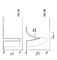
- FIG. 3A shows the effect of this pattern jitter more clearly, in the case of a short low input pulse.
- the dashed line in Figure 3A shows a normal low input pulse in the differential input signal V in .
- the dashed line in Figure 3B shows the corresponding differential output signal V out .
- Sufficient time has elapsed by the end of the normal low input pulse to permit the differential output signal V out to reach its normal low level V OL .
- the solid line in Figure 3B shows the differential output signal V out when the differential input signal V in has a short low input pulse, shown by the solid line in Figure 3A, and the low to high transition occurs before the differential output signal V out reaches V OL .
- the difference between the dashed and solid lines is time jitter, as shown.
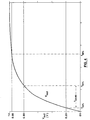
- Figure 4 shows the differential output signal V out , the 20% to 80% rise time of the differential output signal V out for the prior art cable driver 20 (shown in Figure 1) and the 2% settling time (i.e. the 98% rise time, t 98% ) of the differential output signal V out . Since the 20% to 80% rise time of the cable driver must exceed the specified minimum threshold, the maximum data rate which may be transmitted using the prior art cable driver 20 will be dependent on the ratio of the 20% to 80% rise time to the 2% settling time of the differential output signal V out .
- the maximum data rate which may be transmitted on a transmission line could also be increased, without introducing any additional electromagnetic radiation and without increasing jitter.
- Figure 5 shows an improved cable driver 120, according to the present invention.
- the improved cable driver 120 comprises an input port 122, an output port 144, two resistors 128 and 130 and five switching stages SS1, SS2, SS3, SS4 and SS5 coupled in series by four delay stages, D1, D2, D3 and D4.
- Input port 122 comprises input terminals 158 and 160.
- Output port 144 comprises output terminals 146 and 148.
- Resistor 128, which has resistance R 128 is coupled between V CC and node 148 and resistor 130, which has resistance R 130' is coupled between V CC and node 146.
- Resistors 128 and 130 will be chosen to match the impedance of the transmission line to which the improved cable driver 120 is coupled. This eliminates the need for emitter follower output stages, so the associated problems of ringing and overshoot are avoided.
- Switching stage SS1 comprises a current source 162 and a switch 164.
- Current source 162 is coupled between switch 164 and ground.
- Switch 164 is responsive to a differential input signal V in received at input port 122 and may couple current source 162 to node H1 or to node L1.
- Node H1 is coupled to output terminal 148 and node L1 is coupled to output terminal 146.
- Switching stages SS2, SS3, SS4 and SS5 each similarly comprise a current source 166, 170, 174 or 178, respectively, and a switch 168, 172, 176 or 180, respectively. These current sources and switches are coupled together and coupled to ground and to output terminals 148 and 146 in the same manner as current source 162 and switch 164.
- Delay stage D1 is coupled to input port 122 at nodes 182 and 184 and provides a delayed signal V in-1 responsive to input signal V in at nodes 198 and 200.
- Switch 168 is coupled to nodes 198 and 200 and is responsive to signal V in-1 and may connect current source 166 to terminals H2 or L2.
- Delay stages D2, D3 and D4 generate sequentially delayed signals V in-2 , V in-3 and V in-4 corresponding to V in and V in-1 . They are similarly coupled between switches 168 and 172, 172 and 176 and 176 and 180 respectively such that each subsequent switch 172, 176 or 180 receives a signal corresponding to differential input signal V in-2 , V in-3 , V in-4 at a later time than the preceding switch.
- the improved cable driver 120 will typically be configured to produce a differential output signal V out at output terminals 146 and 148.
- the improved cable driver operates as follows.
- a differential input signal V in is received at input terminals 158 and 160 and is directed to switch 164.
- Switch 164 is responsive to differential input signal V in . If V in is high (i.e. V 160 > V 158 ), switch 164 will couple current source 162 to node H1 and conversely, if V in is low (i.e. V 160 ⁇ V 158 ), switch 164 will couple current source 162 to node L1.
- Delay stage D1 provides a delayed signal V in-1 corresponding to input signal V in at nodes 198 and 200.
- Switch 168 is responsive to signal V in-1 . If V in-1 is high, switch 168 will couple current source 166 to node H2 and conversely, if V in-1 is low, switch 168 will couple current source 166 to node L2. In this manner, current sources 162 and 166 will be coupled to the same output terminal 146 or 148.
- switches 172, 176 and 180 are responsive to the delayed signals provided by delay stages D2, D3 and D4, respectively, and will couple current sources 170, 174 and 178, respectively, to the same output terminal 146 or 148 as current sources 162 and 166.
- differential output signal V out will be equal to V OH .
- switch 164 On the high to low transition of V in , switch 164 will switch current source 162 from terminal H1 to L1.
- Delay stage D1 will, after its configured delay period, produce a high to low transition at terminals 198 and 200.
- This process will continue until the delay periods of all four delay stages D1, D2, D3 and D4 have elapsed, all five switches 164, 168, 172, 176 and 180 have respectively coupled 162, 166, 170, 174 and 178 to output terminal 146 and V out has fallen to V OL , as defined above.
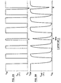
- Figure 6A shows the transitions of switches 164, 168, 172, 176 and 180 from their respective H nodes to their respective L nodes in response to a high to low transition of the differential input signal.
- Figure 6B shows the corresponding high to low transition of V out .
- Switches 164, 168, 172, 176 and 180 are non-ideal switches with a finite transition time. The transition time of switches 164, 168, 172, 176 and 180 and the delay times of delay stages D1, D2, D3 and D4 are preferentially chosen to ensure that the differential output signal V out is substantially linear. At the same time, the 20% to 80% rise and fall times of the differential output signal V out must exceed the specified minimum time.
- the output signal V out will appear as a staircase signal with each step being separated by the delay of the respective delay stages D1, D2, D3 and D4.
- Increasing the transition time of the switches 164, 168, 172, 176 and 180 will provide a smooth transition, improving the linearity of differential output signal V out .
- the differential output signal V out may be made substantially linear by making appropriate choices in the design of the switching stages SS1, SS2, SS3, SS4 and SS5 and delay stages D1, D2, D3 and D4.
- a substantially linear differential output signal V out may be achieved if the delay time between the corresponding signals V in , V in-1, V in-2 , V in-3 and V in-4 is 70ps and the transition time of the switches 164, 168, 172, 176 and 180 is 150 ps. This will provide a differential output signal with a transition time of approximately 220 ps.
- switches 164, 168, 172, 176 and 180 When a low to high transition of V in occurs subsequently, switches 164, 168, 172, 176 and 180 will couple their respective current sources 162, 166, 170, 174 and 178 to output terminal 148 and differential output signal will return to its initial high output level V OH .
- the ratio of the 20% to 80% rise time of V out to the 2% settling time i.e. the 98% rise time
- the 20% to 80% rise time or fall time of the differential output signal V out must exceed a minimum time period. If both the prior art cable driver 20 and the improved cable driver 120 are (1) configured to operate with this minimum 20% to 80% minimum rise/fall time and (2) receive an input which allows them the meet the requirement that the differential output signal V out must settle to with 2% of its steady state value (in order to reduce time jitter, as described above), the improved cable driver 120 will be capable of carrying a higher data rate than the prior art cable driver 20.
- the improved cable driver 120 is capable of carrying a data rate 1.73 times higher than the prior art cable driver 20, without increasing the generation of electromagnetic radiation or increasing jitter in the differential output signal V out .
- One skilled. in the art will recognize that if the particular application in which improved cable driver 120 requires that the jitter in the differential output signal V out be less than 1.46%, as calculated above, the benefit of the invention will be commensurately greater.
- Switch 164 comprises a differential amplifier stage 220 and current source 162 comprises current mirror 222.
- Current mirror 222 comprises transistor Q5, diode connected transistor Q6 and reference current source 224, which are connected in the well known current mirror configuration.
- the bases of transistors Q5 and Q6 are coupled together and the emitters of transistors Q5 and Q6 are connected to a voltage source -V EE .
- the collector of transistor Q6 is coupled to V CC through reference current source 224.
- the current drawn by transistor Q5 through differential amplifier stage 220 will depend on the current of current source 224 in known manner.
- Differential amplifier stage 220 comprises two transistors Q 3 and Q 4 , the emitters of which are connected together.
- the base of transistor Q 3 is coupled to input terminal 158 and the base of transistor Q 4 is coupled to input terminal 160.
- the collector of transistor Q 3 comprises node L1 and the collector of transistor Q 4 comprises node H1.
- the emitters of transistors Q 3 and Q 4 are coupled to the collector of transistor Q 5 .
- the bases of transistors Q 3 and Q 4 are coupled to input terminals 158 and 160, respectively and receive the differential input signal across their bases.
- One skilled in the art will be familiar with the operation of the differential amplifier stage 220 and the current mirror 222 and will understand the switching operation provided by the switching stage SS1.
- Delay stage D1 is comprised of a differential amplifier consisting of transistors Q7 and Q8, resistors 226 and 228 and a current mirror comprising transistors Q9, diode connected transistor Q10 and reference current source 230.
- the emitters of transistors Q7 and Q8 are connected together and to the collector of transistor Q9.
- the base of transistor Q9 is coupled the base of transistor Q10.
- the collector of transistor Q10 is couple to V CC through reference current source 230.
- the emitters of the transistors Q9 and Q10 are connected to -V EE .
- the collectors of transistors Q7 and Q8 are coupled to a voltage source V DD through resistors 226 and 228, respectively.
- Transistors Q7 and Q8 receive the differential input signal V in across their bases, which are connected to input terminals 160 and 158 respectively.
- the collectors of transistors Q7 and Q8 are coupled to nodes 200 and 198 respectively.
- Q7 and Q8 as a differential amplifier will produce signal V in-1 at nodes 198 and 200 (as discussed above) responsive to the differential input signal V in , but delayed in time.
- the length of the delay will depend on the current of current source Q9, which will depend on the current of reference current source 230 in known manner, the resistance of resistors 226 and 228 and other characteristics of the bipolar technology in which the cable driver circuit is realized.
- One skilled in the art will be capable of selecting appropriate components to ensure that the transitions of the differential output signal are substantially linear.
Landscapes
- Engineering & Computer Science (AREA)
- Power Engineering (AREA)
- Computer Networks & Wireless Communication (AREA)
- Signal Processing (AREA)
- Physics & Mathematics (AREA)
- Spectroscopy & Molecular Physics (AREA)
- Dc Digital Transmission (AREA)
- Logic Circuits (AREA)
- Electronic Switches (AREA)
- Control Of Indicators Other Than Cathode Ray Tubes (AREA)
Claims (12)
- Kabeltreiber, umfassend:(a) einen Eingangsanschluss (122) zum Empfangen eines Eingangssignals (Vin), welcher erste und zweite Eingangsklemmen (158 und 160) umfasst;(b) einen Ausgangsanschluss (144) zum Senden eines Ausgangssignals (Vout) auf einer Übertragungsleitung, welcher erste und zweite Ausgangsklemmen (148 und 146) umfasst;(c) einen ersten Widerstand (128) und einen zweiten Widerstand (130) zum Definieren des Ausgangssignals (Vout) an dem Ausgangsanschluss (144), wobei der erste Widerstand (128) zwischen eine Spannungsquelle (VDD) und die erste Ausgangsklemme (148) geschaltet ist und der zweite Widerstand (130) zwischen die Spannungsquelle (VDD) und die zweite Ausgangsklemme (146) geschaltet ist;(d) eine Mehrzahl von Schaltstufen (SS1, SS2, ...), wobei jede der Schaltstufen (SS1, SS2, ...) einen Schalter (164, 168, ...) und eine Stromquelle (162, 166, ...), die mit dem Schalter (164, 168, ...) verbunden ist, zum Erzeugen eines Stroms umfasst, wobei die Stromquelle (162, 166, ...) zum Steuern der Schaltzeit des verbundenen Schalters (164, 168, ...) an ihren verbundenen Schalter (164, 168, ...) gekoppelt ist und jeder der Schalter (164, 168, ...) an den Ausgangsanschluss (144) gekoppelt ist, wobei die Mehrzahl von Schaltstufen (SS1, SS2, ...) eine erste Schaltstufe (SS1) umfasst;(e) eine Mehrzahl von Verzögerungsstufen (D1, D2, ...) zum Bereitstellen einer Verzögerungszeit;(f) wobei die erste Schaltstufe (SS1) an den Eingangsanschluss (122) gekoppelt ist und die restlichen Schaltstufen (SS2, ...) in Reihe geschaltet sind, wobei eine der Verzögerungsstufen (D1, D2, ...) so zwischen jedes aufeinander folgende Paar der Schaltstufen (SS1 und SS2, SS3 und SS4, ...) geschaltet ist, dass jede Verzögerungsstufe (D1, D2, ...) an eine vorhergehende Schaltstufe (SS1, SS2, ...) und eine nachfolgende Schaltstufe (SS2, SS3, ...) gekoppelt ist;(g) die Verzögerungszeiten jeder der Verzögerungsstufen (D1, D2, ...) gleich sind;
dadurch gekennzeichnet, dass:(h) die Ströme jeder Stromquelle (162, 166, ...) gleich sind; und(i) die Verzögerungszeiten und die Ströme so ausgewählt werden, dass die Anstiegs- und Abfallzeiten eines ausgewählten Abschnitts des Ausgangssignals (Vout) eine ausgewählte Dauer überschreiten und der ausgewählte Abschnitt des Ausgangssignals linear ist. - Kabeltreiber nach Anspruch 1, wobei der ausgewählte Abschnitt der 20 bis 80%igen Anstiegszeit des Ausgangssignals (Vout) entspricht.
- Kabeltreiber nach Anspruch 1 oder 2, wobei die ersten und zweiten Widerstände Resistoren (128 und 130) umfassen.
- Kabeltreiber nach Anspruch 1 oder 2, wobei die ersten und zweiten Widerstände einen Widerstand gleich zueinander und gleich zur Impedanz der Übertragungsleitung aufweisen.
- Kabeltreiber nach Anspruch 1 oder 2, wobei jeder der Schalter (164, 168, ...) ein Differenzialverstärker (220) ist.
- Kabeltreiber nach Anspruch 5, wobei der Differenzialverstärker (220) erste und zweite Schalttransistoren (Q3 und Q4) umfasst, wobei jeder der ersten und zweiten Schalttransistoren (Q3 und Q4) einen Emitter, einen Basiseingang und einen Kollektorausgang aufweisen und wobei die Emitter jedes der ersten und zweiten Schalttransistoren (Q3 und Q4) aneinander gekoppelt sind.
- Kabeltreiber nach Anspruch 6, wobei die Stromquelle (162, 164, ...) jeder Schaltstufe (SS1, SS2, ...) an die Emitter der ersten und zweiten Schalttransistoren derselben Schaltstufe (SS1, SS2, ...) gekoppelt ist und wobei jede der Stromquellen (162, 164, ...) eine Stromspiegelschaltung (Q5) ist, welche durch eine gemeinsame Referenzstromquelle (224) gesteuert wird.
- Kabeltreiber nach Anspruch 6, wobei der Kollektorausgang jedes ersten Schalttransistors (Q3) an die erste Ausgangsklemme (148) gekoppelt ist und der Kollektorausgang jedes zweiten Schalttransistors (Q4) an die zweite Ausgangsklemme (146) gekoppelt ist.
- Kabeltreiber nach Anspruch 1 oder 2, wobei jede der Verzögerungsstufen (D1, D2, ...) erste und zweite Verzögerungstransistoren (Q8 und Q7) umfasst, wobei jeder der Verzögerungstransistoren (Q8 und Q7) einen Kollektorausgang, einen Basiseingang und einen Emitter aufweist und wobei die Emitter der ersten und zweiten Verzögerungstransistoren (Q8 und Q7) aneinander und an eine Stromquelle (Q9) gekoppelt sind.
- Kabeltreiber nach Anspruch 9, wobei der Kollektorausgang des ersten Verzögerungstransistors (Q8) durch einen ersten Resistor (228) an eine Spannungsquelle (VDD) gekoppelt ist und der Kollektorausgang des zweiten Verzögerungstransistors (Q7) durch einen zweiten Resistor (226) an eine Spannungsquelle (VDD) gekoppelt ist und wobei die Verzögerungszeit jeder Verzögerungsstufe (D1, D2, ...) durch Auswählen des Widerstands der ersten und zweiten Resistoren (Q8 und Q7) und des Stroms der Stromquelle (Q9) geregelt wird.
- Kabeltreiber nach Anspruch, 6, 7 oder 8, wobei jede der Verzögerungsstufen (D1, D2, ...) erste und zweite Verzögerungstransistoren (Q7 und Q8) umfasst, wobei jeder der Verzögerungstransistoren (Q7 und Q8) einen Kollektorausgang, einen Basiseingang und einen Emitter aufweist und wobei die Emitter der ersten und zweiten Verzögerungstransistoren (Q7 und Q8) aneinander und an eine Stromquelle (Q9) gekoppelt sind.
- Kabeltreiber nach Anspruch 11, wobei:(a) die Basiseingänge der ersten und zweiten Schalttransistoren (Q3 und Q4) der ersten Schaltstufe (SS1) an die ersten beziehungsweise zweiten Eingangsklemmen (158 und 160) gekoppelt sind;(b) für jede Verzögerungsstufe (D1, D2, ...) die Basiseingänge der ersten und zweiten Verzögerungstransistoren (Q8 und Q7) an die Basiseingänge der ersten und zweiten Schalttransistoren (Q3 und Q4) der vorhergehenden Schaltstufe (SS1, SS2, ...) gekoppelt sind;(c) für jede Verzögerungsstufe (D1, D2, ...) die Kollektorausgänge der ersten und zweiten Verzögerungstransistoren (Q8 und Q7) an die Basiseingänge der ersten und zweiten Schalttransistoren (Q3 und Q4) der nachfolgenden Schaltstufe (SS2, SS3, ...) gekoppelt sind.
Priority Applications (1)
| Application Number | Priority Date | Filing Date | Title |
|---|---|---|---|
| DK99900846T DK1050137T3 (da) | 1998-01-21 | 1999-01-19 | Ledningsdriver med lineære overgange |
Applications Claiming Priority (3)
| Application Number | Priority Date | Filing Date | Title |
|---|---|---|---|
| US10194 | 1998-01-21 | ||
| US09/010,194 US6288592B1 (en) | 1998-01-21 | 1998-01-21 | Cable driver with controlled linear rise and fall |
| PCT/CA1999/000031 WO1999038296A1 (en) | 1998-01-21 | 1999-01-19 | Line driver with linear transitions |
Publications (2)
| Publication Number | Publication Date |
|---|---|
| EP1050137A1 EP1050137A1 (de) | 2000-11-08 |
| EP1050137B1 true EP1050137B1 (de) | 2004-11-24 |
Family
ID=21744426
Family Applications (1)
| Application Number | Title | Priority Date | Filing Date |
|---|---|---|---|
| EP99900846A Expired - Lifetime EP1050137B1 (de) | 1998-01-21 | 1999-01-19 | Leitungstreiber mit linearen übergängen |
Country Status (8)
| Country | Link |
|---|---|
| US (1) | US6288592B1 (de) |
| EP (1) | EP1050137B1 (de) |
| JP (1) | JP2002502147A (de) |
| AT (1) | ATE283596T1 (de) |
| AU (1) | AU2042599A (de) |
| CA (1) | CA2318934A1 (de) |
| DE (1) | DE69922161T2 (de) |
| WO (1) | WO1999038296A1 (de) |
Families Citing this family (11)
| Publication number | Priority date | Publication date | Assignee | Title |
|---|---|---|---|---|
| KR100419149B1 (ko) * | 1999-09-22 | 2004-02-14 | 엘지전자 주식회사 | 동기식 시스템에서 이엠아이 발생 방지를 위한 동기 신호 전송 제어 장치 및 방법 |
| US7433665B1 (en) | 2000-07-31 | 2008-10-07 | Marvell International Ltd. | Apparatus and method for converting single-ended signals to a differential signal, and transceiver employing same |
| US6462688B1 (en) * | 2000-12-18 | 2002-10-08 | Marvell International, Ltd. | Direct drive programmable high speed power digital-to-analog converter |
| US6775529B1 (en) | 2000-07-31 | 2004-08-10 | Marvell International Ltd. | Active resistive summer for a transformer hybrid |
| USRE41831E1 (en) * | 2000-05-23 | 2010-10-19 | Marvell International Ltd. | Class B driver |
| US7312739B1 (en) | 2000-05-23 | 2007-12-25 | Marvell International Ltd. | Communication driver |
| US7606547B1 (en) | 2000-07-31 | 2009-10-20 | Marvell International Ltd. | Active resistance summer for a transformer hybrid |
| US6832277B2 (en) * | 2001-08-02 | 2004-12-14 | Sun Microsystems, Inc. | Method and apparatus for transmitting data that utilizes delay elements to reduce capacitive coupling |
| US8059724B2 (en) | 2007-03-11 | 2011-11-15 | Sandisk Il Ltd | Method and system for reducing common mode noise interference in a differential communication channel |
| US20090153688A1 (en) * | 2007-12-13 | 2009-06-18 | Gennum Corporation | Digital Video Cable Driver |
| JP5358349B2 (ja) * | 2009-08-26 | 2013-12-04 | ザインエレクトロニクス株式会社 | データ送信回路及びデータ通信装置 |
Family Cites Families (9)
| Publication number | Priority date | Publication date | Assignee | Title |
|---|---|---|---|---|
| JPH02303242A (ja) * | 1989-05-17 | 1990-12-17 | Nec Corp | バス中継装置 |
| JPH0752870B2 (ja) * | 1990-05-17 | 1995-06-05 | 日本電装株式会社 | 通信装置 |
| US5287386A (en) | 1991-03-27 | 1994-02-15 | Thinking Machines Corporation | Differential driver/receiver circuit |
| US5327021A (en) | 1991-06-10 | 1994-07-05 | Shinko Electric Ind., Co., Ltd. | Waveform synthesizing circuit |
| US5446914A (en) * | 1992-12-22 | 1995-08-29 | National Semiconductor Corporation | Twisted pair and attachment unit interface (AUI) coding and transceiving circuit with full duplex, testing, and isolation modes |
| US5410188A (en) | 1992-12-22 | 1995-04-25 | National Semiconductor Corporation | Enhanced integrated waveshaping circuit |
| US5408497A (en) | 1993-07-14 | 1995-04-18 | Echelon Corporation | Transceiver for transmitting and receiving stair-stepped sinusoidal waveforms |
| US5534801A (en) | 1994-01-24 | 1996-07-09 | Advanced Micro Devices, Inc. | Apparatus and method for automatic sense and establishment of 5V and 3.3V operation |
| GB2305082B (en) | 1995-09-06 | 1999-10-06 | At & T Corp | Wave shaping transmit circuit |
-
1998
- 1998-01-21 US US09/010,194 patent/US6288592B1/en not_active Expired - Fee Related
-
1999
- 1999-01-19 DE DE69922161T patent/DE69922161T2/de not_active Expired - Fee Related
- 1999-01-19 WO PCT/CA1999/000031 patent/WO1999038296A1/en not_active Ceased
- 1999-01-19 EP EP99900846A patent/EP1050137B1/de not_active Expired - Lifetime
- 1999-01-19 CA CA002318934A patent/CA2318934A1/en not_active Abandoned
- 1999-01-19 JP JP2000529063A patent/JP2002502147A/ja active Pending
- 1999-01-19 AU AU20425/99A patent/AU2042599A/en not_active Abandoned
- 1999-01-19 AT AT99900846T patent/ATE283596T1/de not_active IP Right Cessation
Also Published As
| Publication number | Publication date |
|---|---|
| US6288592B1 (en) | 2001-09-11 |
| DE69922161T2 (de) | 2005-05-04 |
| ATE283596T1 (de) | 2004-12-15 |
| DE69922161D1 (de) | 2004-12-30 |
| AU2042599A (en) | 1999-08-09 |
| EP1050137A1 (de) | 2000-11-08 |
| JP2002502147A (ja) | 2002-01-22 |
| WO1999038296A1 (en) | 1999-07-29 |
| CA2318934A1 (en) | 1999-07-29 |
Similar Documents
| Publication | Publication Date | Title |
|---|---|---|
| EP0763917B1 (de) | Leitungstreiber mit Impulsformer | |
| EP1050137B1 (de) | Leitungstreiber mit linearen übergängen | |
| US6838943B2 (en) | Input follower system and method | |
| US7176823B2 (en) | Gigabit ethernet line driver and hybrid architecture | |
| US20020079923A1 (en) | Output slew rate control for a differential transmission line driver | |
| US6721379B1 (en) | DAC/Driver waveform generator with phase lock rise time control | |
| US4994690A (en) | Split level bus | |
| US6625206B1 (en) | Simultaneous bidirectional data transmission system and method | |
| US7974304B2 (en) | Out of band signaling enhancement for high speed serial driver | |
| US4947061A (en) | CMOS to ECL output buffer circuit | |
| US6069511A (en) | Digital slew rate and duty cycle control circuit and method | |
| US5677642A (en) | Signal generator with supply voltage tolerance | |
| US6424188B2 (en) | Signal transmission device | |
| EP3826247B1 (de) | Sender mit entzerrung | |
| GB2214019A (en) | A distributed precharge wire-or bus | |
| US6366125B1 (en) | Digital output circuit | |
| US5587679A (en) | Pulse generator including slew rate controller without complementary transistors | |
| US6246734B1 (en) | Vehicle communication system | |
| EP0518625A2 (de) | Wellenform-Synthetisierungsschaltung | |
| US6292035B1 (en) | Signal transmission device | |
| KR102785156B1 (ko) | 떨림 억제 회로를 포함하는 차량용 통신 시스템 | |
| US20250047532A1 (en) | Communication device | |
| US6980588B2 (en) | Apparatus for handling high speed data communication signals and method for manufacture thereof | |
| CN119341527A (zh) | 一种模拟延时调节电路及方法 | |
| JP2639306B2 (ja) | シフトレジスタ回路 |
Legal Events
| Date | Code | Title | Description |
|---|---|---|---|
| PUAI | Public reference made under article 153(3) epc to a published international application that has entered the european phase |
Free format text: ORIGINAL CODE: 0009012 |
|
| 17P | Request for examination filed |
Effective date: 20000827 |
|
| AK | Designated contracting states |
Kind code of ref document: A1 Designated state(s): AT CH DE DK FR GB IT LI NL |
|
| 17Q | First examination report despatched |
Effective date: 20010330 |
|
| GRAP | Despatch of communication of intention to grant a patent |
Free format text: ORIGINAL CODE: EPIDOSNIGR1 |
|
| GRAS | Grant fee paid |
Free format text: ORIGINAL CODE: EPIDOSNIGR3 |
|
| GRAA | (expected) grant |
Free format text: ORIGINAL CODE: 0009210 |
|
| AK | Designated contracting states |
Kind code of ref document: B1 Designated state(s): AT CH DE DK FR GB IT LI NL |
|
| PG25 | Lapsed in a contracting state [announced via postgrant information from national office to epo] |
Ref country code: LI Free format text: LAPSE BECAUSE OF FAILURE TO SUBMIT A TRANSLATION OF THE DESCRIPTION OR TO PAY THE FEE WITHIN THE PRESCRIBED TIME-LIMIT Effective date: 20041124 Ref country code: CH Free format text: LAPSE BECAUSE OF FAILURE TO SUBMIT A TRANSLATION OF THE DESCRIPTION OR TO PAY THE FEE WITHIN THE PRESCRIBED TIME-LIMIT Effective date: 20041124 Ref country code: AT Free format text: LAPSE BECAUSE OF FAILURE TO SUBMIT A TRANSLATION OF THE DESCRIPTION OR TO PAY THE FEE WITHIN THE PRESCRIBED TIME-LIMIT Effective date: 20041124 |
|
| REG | Reference to a national code |
Ref country code: GB Ref legal event code: FG4D |
|
| REG | Reference to a national code |
Ref country code: CH Ref legal event code: EP |
|
| REF | Corresponds to: |
Ref document number: 69922161 Country of ref document: DE Date of ref document: 20041230 Kind code of ref document: P |
|
| PGFP | Annual fee paid to national office [announced via postgrant information from national office to epo] |
Ref country code: DK Payment date: 20050126 Year of fee payment: 7 Ref country code: DE Payment date: 20050126 Year of fee payment: 7 |
|
| PGFP | Annual fee paid to national office [announced via postgrant information from national office to epo] |
Ref country code: FR Payment date: 20050127 Year of fee payment: 7 |
|
| PGFP | Annual fee paid to national office [announced via postgrant information from national office to epo] |
Ref country code: NL Payment date: 20050131 Year of fee payment: 7 |
|
| REG | Reference to a national code |
Ref country code: DK Ref legal event code: T3 |
|
| REG | Reference to a national code |
Ref country code: CH Ref legal event code: PL |
|
| PLBE | No opposition filed within time limit |
Free format text: ORIGINAL CODE: 0009261 |
|
| STAA | Information on the status of an ep patent application or granted ep patent |
Free format text: STATUS: NO OPPOSITION FILED WITHIN TIME LIMIT |
|
| 26N | No opposition filed |
Effective date: 20050825 |
|
| ET | Fr: translation filed | ||
| PG25 | Lapsed in a contracting state [announced via postgrant information from national office to epo] |
Ref country code: FR Free format text: LAPSE BECAUSE OF NON-PAYMENT OF DUE FEES Effective date: 20060131 Ref country code: DK Free format text: LAPSE BECAUSE OF NON-PAYMENT OF DUE FEES Effective date: 20060131 |
|
| PGFP | Annual fee paid to national office [announced via postgrant information from national office to epo] |
Ref country code: IT Payment date: 20060131 Year of fee payment: 8 |
|
| PG25 | Lapsed in a contracting state [announced via postgrant information from national office to epo] |
Ref country code: NL Free format text: LAPSE BECAUSE OF NON-PAYMENT OF DUE FEES Effective date: 20060801 Ref country code: DE Free format text: LAPSE BECAUSE OF NON-PAYMENT OF DUE FEES Effective date: 20060801 |
|
| REG | Reference to a national code |
Ref country code: DK Ref legal event code: EBP |
|
| NLV4 | Nl: lapsed or anulled due to non-payment of the annual fee |
Effective date: 20060801 |
|
| REG | Reference to a national code |
Ref country code: FR Ref legal event code: ST Effective date: 20060929 |
|
| GBPC | Gb: european patent ceased through non-payment of renewal fee |
Effective date: 20070119 |
|
| PG25 | Lapsed in a contracting state [announced via postgrant information from national office to epo] |
Ref country code: GB Free format text: LAPSE BECAUSE OF NON-PAYMENT OF DUE FEES Effective date: 20070119 |
|
| PGFP | Annual fee paid to national office [announced via postgrant information from national office to epo] |
Ref country code: GB Payment date: 20060125 Year of fee payment: 8 |
|
| PG25 | Lapsed in a contracting state [announced via postgrant information from national office to epo] |
Ref country code: IT Free format text: LAPSE BECAUSE OF NON-PAYMENT OF DUE FEES Effective date: 20070119 |