EP1050909A1 - Dispositif de cellule solaire et son procede de production - Google Patents
Dispositif de cellule solaire et son procede de production Download PDFInfo
- Publication number
- EP1050909A1 EP1050909A1 EP99900665A EP99900665A EP1050909A1 EP 1050909 A1 EP1050909 A1 EP 1050909A1 EP 99900665 A EP99900665 A EP 99900665A EP 99900665 A EP99900665 A EP 99900665A EP 1050909 A1 EP1050909 A1 EP 1050909A1
- Authority
- EP
- European Patent Office
- Prior art keywords
- semiconductor layer
- type semiconductor
- transparent oxide
- oxide electrode
- solar cell
- Prior art date
- Legal status (The legal status is an assumption and is not a legal conclusion. Google has not performed a legal analysis and makes no representation as to the accuracy of the status listed.)
- Withdrawn
Links
Images



Classifications
-
- H—ELECTRICITY
- H10—SEMICONDUCTOR DEVICES; ELECTRIC SOLID-STATE DEVICES NOT OTHERWISE PROVIDED FOR
- H10F—INORGANIC SEMICONDUCTOR DEVICES SENSITIVE TO INFRARED RADIATION, LIGHT, ELECTROMAGNETIC RADIATION OF SHORTER WAVELENGTH OR CORPUSCULAR RADIATION
- H10F71/00—Manufacture or treatment of devices covered by this subclass
- H10F71/138—Manufacture of transparent electrodes, e.g. transparent conductive oxides [TCO] or indium tin oxide [ITO] electrodes
-
- H—ELECTRICITY
- H10—SEMICONDUCTOR DEVICES; ELECTRIC SOLID-STATE DEVICES NOT OTHERWISE PROVIDED FOR
- H10F—INORGANIC SEMICONDUCTOR DEVICES SENSITIVE TO INFRARED RADIATION, LIGHT, ELECTROMAGNETIC RADIATION OF SHORTER WAVELENGTH OR CORPUSCULAR RADIATION
- H10F10/00—Individual photovoltaic cells, e.g. solar cells
- H10F10/10—Individual photovoltaic cells, e.g. solar cells having potential barriers
- H10F10/17—Photovoltaic cells having only PIN junction potential barriers
-
- H—ELECTRICITY
- H10—SEMICONDUCTOR DEVICES; ELECTRIC SOLID-STATE DEVICES NOT OTHERWISE PROVIDED FOR
- H10F—INORGANIC SEMICONDUCTOR DEVICES SENSITIVE TO INFRARED RADIATION, LIGHT, ELECTROMAGNETIC RADIATION OF SHORTER WAVELENGTH OR CORPUSCULAR RADIATION
- H10F71/00—Manufacture or treatment of devices covered by this subclass
-
- H—ELECTRICITY
- H10—SEMICONDUCTOR DEVICES; ELECTRIC SOLID-STATE DEVICES NOT OTHERWISE PROVIDED FOR
- H10F—INORGANIC SEMICONDUCTOR DEVICES SENSITIVE TO INFRARED RADIATION, LIGHT, ELECTROMAGNETIC RADIATION OF SHORTER WAVELENGTH OR CORPUSCULAR RADIATION
- H10F77/00—Constructional details of devices covered by this subclass
- H10F77/20—Electrodes
- H10F77/244—Electrodes made of transparent conductive layers, e.g. transparent conductive oxide [TCO] layers
-
- Y—GENERAL TAGGING OF NEW TECHNOLOGICAL DEVELOPMENTS; GENERAL TAGGING OF CROSS-SECTIONAL TECHNOLOGIES SPANNING OVER SEVERAL SECTIONS OF THE IPC; TECHNICAL SUBJECTS COVERED BY FORMER USPC CROSS-REFERENCE ART COLLECTIONS [XRACs] AND DIGESTS
- Y02—TECHNOLOGIES OR APPLICATIONS FOR MITIGATION OR ADAPTATION AGAINST CLIMATE CHANGE
- Y02E—REDUCTION OF GREENHOUSE GAS [GHG] EMISSIONS, RELATED TO ENERGY GENERATION, TRANSMISSION OR DISTRIBUTION
- Y02E10/00—Energy generation through renewable energy sources
- Y02E10/50—Photovoltaic [PV] energy
- Y02E10/548—Amorphous silicon PV cells
Definitions
- the present invention relates to a silicon solar cell device achieving high conversion efficiency by improving open circuit voltage of the silicon solar cell device and a fabricating method of the same.
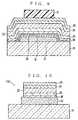
- FIG. 10 is a sectional view showing the structure of a conventional solar cell device 102.
- the solar cell device 102 has a structure in which a transparent oxide electrode 12 is formed on the surface of an insulating substrate 10 which is a transparent glass substrate, and a p-type semiconductor layer 18, a buffer layer 20, an intrinsic semiconductor layer 22, an n-type semiconductor layer 24, and a metal electrode 26 are laminated in that order on to the surface of the transparent oxide electrode 12 into a laminated structure.
- the insulating substrate 10 transmits light incident from the surface on the side thereof (the lower side in the drawing), on which the transparent oxide electrode 12 is not formed, to the transparent oxide electrode 12.
- the transparent oxide electrode 12 is formed to lead light (mainly sunlight) incident through the insulating substrate 10 to the intrinsic semiconductor layer 22 through the p-type semiconductor layer 18 and the buffer layer 20 and to keep ohmic contact with the p-type semiconductor layer 18.
- the p-type semiconductor layer 18 is a layer composed of a p-type semiconductor, which is provided to lead carriers, produced in the intrinsic semiconductor layer 22 by the incident light, to the transparent oxide electrode 12.
- the buffer layer 20 functions as a buffer layer for preventing a forbidden band width of the intrinsic semiconductor layer 22 from narrowing due to the mixing of p-type impurities (boron) contained in the p-type semiconductor layer 18, into the intrinsic semiconductor layer 22.
- the intrinsic semiconductor layer 22 is a layer made of an intrinsic semiconductor for producing caters by absorbing incident light.
- the n-type semiconductor layer 24 is a layer made of an n-type semiconductor provided to lead the carriers produced in the intrinsic semiconductor layer 22 to the metal electrode 26.
- the metal electrode 26 is connected with an interconnection for taking out electromotive force.
- tin oxide film is formed on the insulating substrate 10 to form a transparent oxide electrode 12, and thereafter a photoresist 13 is applied on the entire surface of the tin oxide film.
- the photoresist 13 is exposed and developed with a predetermined mask to remain in a region which is to be the solar cell device 102.
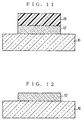
- the transparent oxide electrode 12 is etched by means of a reactive ion etching system with the above photoresist 13 as an etching mask and with hydrogen iodide (HI) and argon (Ar) used as the raw material gas. Removing the photoresist 13 makes a state where the transparent oxide electrode 12 is provided on the surface of the insulating substrate 10 as shown in FIG. 12.
- HI hydrogen iodide
- Ar argon
- the p-type semiconductor layer 18 is formed on the entire surface of the insulating substrate 10 so as to cover the transparent oxide electrode 12, as shown in FIG. 13, by the plasma CVD (chemical-vapor deposition) method.
- mono-silane (SiH 4 ) and diborane (B 2 H 6 ) are used as the raw material gas.
- Methane gas (CH 4 ) is simultaneously introduced to form silicon carbide in the p-type semiconductor layer 18, thereby preventing the forbidden band width of the p-type semiconductor layer 18 from narrowing and the light conversion efficiency from lowering.
- the buffer layer 20 is formed over the entire surface of the p-type semiconductor layer 18.
- the intrinsic semiconductor layer 22 is next formed on the entire surface of the buffer layer 20. This is also carried out by the plasma CVD method with mono-silane (SiH 4 ) as the raw material gas.
- the n-type semiconductor layer 24 is formed on the entire surface of the intrinsic semiconductor layer 22. This is performed by the plasma CVD method with mono-silane (SiH 4 ) and phosphine (PH 3 ) as the raw material gas. Thereafter, a metal film 25 which becomes the metal electrode 26 is formed on the entire surface of the n-type semiconductor layer 24 by the sputtering method and a photoresist 15 is applied on the entire surface of the metal film 25.
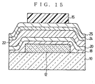
- the photoresist 15 is exposed and developed with a predetermined mask, as shown in FIG. 15, to remain only in a region which is to be the solar cell device 102. Then, the metal film 25 and the respective layers laminated thereunder are etched and removed by the reactive ion etching method using the photoresist 15 as an etching mask, and the photoresist 15 used for the etching mask is also removed.
- the solar cell device 102 can be fabricated as shown in FIG. 10, in which all layers from the p-type semiconductor layer 18, the buffer layer 20, the intrinsic semiconductor layer 22, the n-type semiconductor layer 24 to the metal electrode 26 are laminated in that order on the transparent oxide electrode 12.
- the solar cell device 102 in the prior art can be fabricated by the above fabricating method, the solar cell device 102 has a structure using tin oxide as the transparent oxide electrode 12, and thus it has the following disadvantages regarding the structure. More specifically, tin oxide is a chemically very active substance and has a characteristic of being easy to react with a semiconductor layer laminated on the transparent oxide electrode 12. Accordingly, interdiffusion of atoms tends to occur between the transparent oxide electrode 12 and the p-type semiconductor layer 18, and thus there arise disadvantages that transparency of the transparent oxide electrode 12 deteriorates, resulting in a decrease in transmittance and that deterioration in film quality of an amorphous semiconductor layer (especially, the intrinsic semiconductor layer 22) causes a decrease in open circuit voltage.
- tin oxide is a chemically very active substance and has a characteristic of being easy to react with a semiconductor layer laminated on the transparent oxide electrode 12. Accordingly, interdiffusion of atoms tends to occur between the transparent oxide electrode 12 and the p-type semiconductor layer 18, and
- An object of the present invention is to improve output characteristics of a solar cell device including enhancement of open circuit voltage by solving the disadvantages as described above in the solar cell device and the fabricating method of the same.
- the present invention is characterized by a solar cell device in which a transparent oxide electrode is provided on an insulating substrate, a p-type semiconductor layer, an intrinsic semiconductor layer, and an n-type semiconductor layer are provided over the transparent oxide electrode in that order, and a metal electrode is provided on the n-type semiconductor layer, in which the transparent oxide electrode is provided with a surface treatment layer made by performing oxidative plasma treatment on the surface thereof and the p-type semiconductor layer is provided with the surface treatment layer therebetween to thereby form the solar cell device.
- the provision of the surface treatment layer chemically stabilizes the transparent oxide electrode, thereby improving open circuit voltage.
- the solar cell device it is preferable to form the solar cell device so that a silicon nitride film is provided between the surface treatment layer and the p-type semiconductor layer. Thereby, the transparent oxide electrode is further chemically stabilized.
- side faces of the transparent oxide electrode which are not provided wit the p-type semiconductor layer are formed in a tapered shape gradually inclined outward from the top end thereof toward the insulating substrate. Thereby, a break in the interconnection and a short circuit of the metal electrode are prevented.
- the present invention is also characterized by a fabricating method of a solar cell device comprising the steps of: forming a transparent oxide electrode on an insulating substrate; forming a surface treatment layer by performing oxidative plasma treatment on the surface of the transparent oxide electrode; forming a p-type semiconductor layer, an intrinsic semiconductor layer, and an n-type semiconductor layer on the surface treatment layer in that order; and forming a metal electrode on the n-type semiconductor layer.
- the transparent oxide electrode is formed so that side faces thereof which are not provided with the p-type semiconductor layer are formed in a tapered shape gradually inclined outward from the top end thereof toward the insulating substrate in the step of forming the transparent oxide electrode.
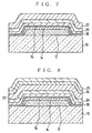
- FIG. 1 Structure of the solar cell device: FIG. 1
- FIG. 1 is a sectional view showing the structure of the solar cell device in the best mode according to the present invention.
- the solar cell device 2 has a structure in which a transparent oxide electrode 12 is provided on the surface of an insulating substrate 10 which is a transparent glass substrate, the surface of the transparent oxide electrode 12 undergoes oxidative plasma treatment to provide a surface treatment layer 14, on which a silicon nitride film 16 is provided, and a p-type semiconductor layer 18, a buffer layer 20, an intrinsic semiconductor layer 22, an n-type semiconductor layer 24, and a metal electrode 26 are laminated in that order on the surface of the silicon nitride film 16 into a laminated structure.
- the insulating substrate 10 is shaped into a plate having a suitable size in width and depth and a suitable thickness and transmits light incident from the surface on the side thereof (the lower side in the drawing), on which the transparent oxide electrode 12 is not formed, to the transparent oxide electrode 12.
- the transparent oxide electrode 12 is formed to lead light (mainly sunlight) incident trough the insulating substrate 10 to the intrinsic semiconductor layer 22 through the surface treatment layer 14, the silicon nitride film 16, the p-type semiconductor layer 18, and the buffer layer 20, and to keep ohmic contact with the p-type semiconductor layer 18, and is connected with an interconnection for taking out generated electromotive force to the outside thereof.
- light mainly sunlight
- the transparent oxide electrode 12 according to the present invention is formed in a tapered shape in which side faces 12a which the p-type semiconductor layer 18 is not provided thereon, are gradually inclined outward from the top end thereof toward the insulating substrate 10. Thereby, a break in the interconnection and a short circuit of the metal electrode 26 is prevented.
- the surface treatment layer 14 is formed by performing oxidative plasma treatment.
- the surface treatment layer 14 functions as a surface stabilizing layer for retarding the reduction of the transparent oxide electrode 12 and for chemically stabilizing the surface of the transparent oxide electrode 12 to improve characteristics of the solar cell device 2. More specifically, the oxidative plasma treatment allows oxygen atoms contained in the surface treatment layer 14 formed by the oxygen atom plasma to unite with not-yet-united tin atoms appearing on the surface of the transparent oxide electrode 12, thereby retarding the union of impurities (boron) contained in the p-type semiconductor layer 18 and the not-yet-united tin atoms (retardation of the reduction). Accordingly, the surface treatment layer 14 stabilizes the surface of the transparent oxide electrode 12.
- the silicon nitride film 16 is formed to prevent mutual diffusion between the transparent oxide electrode 12 and the p-type semiconductor layer 18 and to prevent the reflection of incident sunlight in order to allow sunlight to efficiently stream into the intrinsic semiconductor layer 22.
- the p-type semiconductor layer 18 is a layer composed of a p-type semiconductor which is provided to form an internal electric field for leading camers produced in the intrinsic semiconductor layer 22 by incident light to the transparent oxide electrode 12.
- the buffer layer 20 functions as a buffer layer for preventing a forbidden band width of the intrinsic semiconductor layer 22 from narrowing due to the mixing of the p-type impurities (boron) contained in the p-type semiconductor layer 18 into the intrinsic semiconductor layer 22 and for preventing light absorption efficiency from lowering.
- the intrinsic semiconductor layer 22 is a layer made of an intrinsic semiconductor for producing carriers (pairs of electron and hole) in correspondence with the absorbed energy of incident light.
- the n-type semiconductor layer 24 is a layer composed of an n-type semiconductor provided to form an internal electric field for leading the carriers produced in the intrinsic semiconductor layer 22 to the metal electrode 26.
- the metal electrode 26 is connected with an interconnection for taking out electromotive force.
- the solar cell device 2 having such a structure is used as shown in FIG. 2. More specifically, an interconnection code 27 is connected with the surface of the transparent oxide electrode 12 via the surface treatment layer 14 and an interconnection code 28 is connected with the metal electrode 26, and a load resistance 29 is connected with the interconnection codes 27 and 28.
- the incident light 30 After light 30 streams in from the rear face, which is not provided with the transparent oxide electrode 12, of the insulating substrate 10, the incident light 30 reaches to the intrinsic semiconductor layer 22 from the transparent oxide electrode 12 through the surface treatment layer 14, the silicon nitride film 16, the p-type semiconductor layer 18 and the buffer layer 20.
- the pairs of electrons and holes are produced in the intrinsic semiconductor layer 22.
- the pairs of electrons and holes are separated by an electric field formed by the p-type semiconductor layer 18 and the n-type semiconductor layer 24, whereby electromotive force appears in the transparent oxide electrode 12 and the metal electrode 26.
- the electromotive force can be taken out of the load resistance 29 connected with the solar cell device 2 via the interconnection codes 27 and 28. As a consequence, energy of incident light comes to be converted into electric energy.
- the transparent oxide electrode 12 is provided with the surface treatment layer 14 formed by oxidative plasma treatment on its surface, it is chemically stable by virtue of retardation of the reduction on the surface thereof Accordingly, the transmittancy of the transparent oxide electrode 12 does not lower and the film quality of an amorphous semiconductor layer does not deteriorate, thus improving open circuit voltage to obtain preferable output characteristics as a solar cell device. Moreover, the provision of the silicon nitride film 16 can further stabilize the film quality of the transparent oxide electrode 12, thereby further improving open circuit voltage.
- tin oxide film is formed to form the transparent oxide electrode 12 on the insulating substrate 10 as shown in FIG. 3.
- the above film is formed with a thickness approximately 900 nm by the CVD method.
- the photoresist 13 with the film thickness of about 2.3 ⁇ m is applied over the entire surface of the insulating substrate 10 on which tin oxide film is formed, thereafter the photoresist 13 is exposed and developed with a predetermined mask so as to remain in a region which will become the solar cell device 2.
- the film-formed tin oxide is patterned by being etched by the reactive ion etching system using raw material gas composed of hydrogen iodide (HI) and argon (Ar) with the above photoresist 13 as an etching mask.
- the etching of the film-formed tin oxide is performed so that the side faces 12a which are not covered with the photoresist 13 are formed in a tapered shape gradually inclined outward from the top end thereof toward the insulating substrate 10 in order to prevent a break in the interconnection and a short circuit of the metal electrode 26.
- Removing the photoresist 13, a state where the transparent oxide electrode 12 is provided on the insulating substrate 10 is obtained as shown in FIG. 5.
- oxidative plasma treatment is performed to form the surface treatment layer 14.
- the oxidative plasma treatment is carried out by exposing the transparent oxide electrode 12 to a plasma atmosphere applied with radio-frequency electric power of about 13.56 MHz at 300 W with raw material gas composed of oxygen (O 2 ) and argon (Ar) at a flow ratio of 6:1.
- the surface treatment layer 14 having the film thickness of several nm performed the oxidative plasma treatment is formed not only on the transparent oxide electrode 12 but also on the side faces 12a.
- the silicon nitride film 16 for preventing reflection of incident sunlight is formed with a thickness of about 2 nm over the entire surface of the insulating substrate 10.
- This treatment is carried out by the plasma CVD (chemical-vapor deposition) method with radio-frequency discharge of about 13.56 MHz, using mono-silane (SiH 4 ) and nitrogen (N 2 ) as the raw material gas.
- the p-type semiconductor layer 18 is formed over the entire surface of the insulating substrate 10 in such a manner to cover the silicon nitride film 16 by the plasma CVD (chemical-vapor deposition) method.
- mono-silane (SiH 4 ) and diborane (B 2 H 6 ) are used as the raw material gas and the film thickness of the p-type semiconductor layer 18 is made about 10 nm.
- methane gas (CH 4 ) is introduced to make silicon carbide in the p-type semiconductor layer 18, thereby preventing the forbidden band width of the p-type semiconductor layer 18 from narrowing and preventing the light converting efficiency from lowering.
- the buffer layer 20 is then formed on the entire surface of the p-type semiconductor layer 18. This is carried out by the plasma CVD method with mono-silane (SiH 4 ), methane gas (CH 4 ) and hydrogen (H 2 ) used as the raw material gas, and the film thickness of the buffer layer 20 is made to be about 13 nm.
- the intrinsic semiconductor layer 22 is next formed on the entire surface of the buffer layer 20. This is also carried out by the plasma CVD method with mono-silane (SiH 4 ) as the raw material gas. The film thickness of the intrinsic semiconductor layer 22 is made to be about 600 nm.
- the n-type semiconductor layer 24 is formed on the entire surface of the intrinsic semiconductor layer 22. This is performed by the plasma CVD method with mono-silane (SiH 4 ) and phosphine (PH 3 ) as the raw material gas, in such a manner to grow the n-type semiconductor layer 24 up to about 40 nm in film thickness. Then, the metal film 25 for the metal electrode 26 is formed on the entire surface of the n-type semiconductor layer 24 by the sputtering method. The metal film 25 is formed to be about 200 nm in film thickness with titanium (Ti) as the raw material. Thereafter, a photoresist 17 is applied on the entire surface of the metal film 25 to be about 1.2 ⁇ m in film thickness by the spin coating method.
- SiH 4 mono-silane
- PH 3 phosphine
- Exposing and developing are performed for the photoresist 17 with a predetermined mask, whereby the photoresist 17 is patterned so as to remain only in a region that will become the solar cell device 2 as shown in FIG. 9.
- the metal film 25 is first removed through etching by means of the reactive ion etching system using chlorine (Cl 2 ) and boron trichloride (BCl 3 ) as the etching gas with the above photoresist 17 as an etching mask to form the metal electrode 26.
- the n-type semiconductor layer 24, the intrinsic semiconductor layer 22, the buffer layer 20, the p-type semiconductor layer 18 and the silicon nitride film 16 laminated under the metal electrode 26 are self alignmently etched by means of the reactive ion etching system, using the above photoresist 17 and the metal electrode 26 as an etching mask and sulfur hexafluoride (SF 6 ), carbon tetrafluoride (CF 4 ) and oxygen (O 2 ) for the raw material gas. Thereafter, the photoresist 17 used for the etching mask is removed.
- SF 6 sulfur hexafluoride
- CF 4 carbon tetrafluoride
- O 2 oxygen
- the solar cell device 2 can be fabricated in which the surface treatment layer 14 is formed on the transparent oxide electrode 12, on which the silicon nitride film 16 is formed, and layers from the p-type semiconductor layer 18, the buffer layer 20, the intrinsic semiconductor layer 22, the n-type semiconductor layer 24 to the metal electrode 26 are laminated in that order as shown in FIG. 1.
- the solar cell device according to the present invention is provided with the surface treatment layer by oxidative plasma treatment on the surface of the transparent oxide electrode, whereby the surface of the transparent oxide electrode comes to be chemically stabilized. Accordingly, there are no decreases in transmittance thereof and no deterioration in film quality of the amorphous semiconductor layer, and thus the open circuit voltage is improved resulting in preferable output characteristics as a solar cell device.
- the provision of the silicon nitride film further stabilizes the film quality of the transparent oxide electrode, whereby the open circuit voltage is further improved.
- a solar cell device in which open circuit voltage is improved and which has preferable output characteristics can be easily fabricated.
Landscapes
- Photovoltaic Devices (AREA)
Applications Claiming Priority (3)
| Application Number | Priority Date | Filing Date | Title |
|---|---|---|---|
| JP1007198 | 1998-01-22 | ||
| JP1007198 | 1998-01-22 | ||
| PCT/JP1999/000256 WO1999038216A1 (fr) | 1998-01-22 | 1999-01-22 | Dispositif de cellule solaire et son procede de production |
Publications (2)
| Publication Number | Publication Date |
|---|---|
| EP1050909A1 true EP1050909A1 (fr) | 2000-11-08 |
| EP1050909A4 EP1050909A4 (fr) | 2002-01-30 |
Family
ID=11740150
Family Applications (1)
| Application Number | Title | Priority Date | Filing Date |
|---|---|---|---|
| EP99900665A Withdrawn EP1050909A4 (fr) | 1998-01-22 | 1999-01-22 | Dispositif de cellule solaire et son procede de production |
Country Status (7)
| Country | Link |
|---|---|
| US (1) | US6333456B1 (fr) |
| EP (1) | EP1050909A4 (fr) |
| KR (1) | KR20010033375A (fr) |
| CN (1) | CN1287690A (fr) |
| AU (1) | AU1983499A (fr) |
| BR (1) | BR9907023A (fr) |
| WO (1) | WO1999038216A1 (fr) |
Families Citing this family (10)
| Publication number | Priority date | Publication date | Assignee | Title |
|---|---|---|---|---|
| WO1999038216A1 (fr) * | 1998-01-22 | 1999-07-29 | Citizen Watch Co., Ltd. | Dispositif de cellule solaire et son procede de production |
| KR100374020B1 (ko) * | 2000-09-25 | 2003-02-26 | 학교법인고려중앙학원 | ITO/n형 반도체층 계면에서 터널링 접합을 이용한박막 광전지 및 그 제조방법 |
| JP3906182B2 (ja) * | 2002-06-21 | 2007-04-18 | アスラブ・エス アー | 特に液晶ディスプレイセル又は電気化学光電池である多層セル |
| US7022247B2 (en) * | 2003-03-26 | 2006-04-04 | Union Semiconductor Technology Corporation | Process to form fine features using photolithography and plasma etching |
| EP1939947B1 (fr) * | 2005-08-30 | 2018-11-21 | Kaneka Corporation | Convertisseur photoelectrique a film mince a base de silicium et procede de fabrication de celui-ci |
| JP5470633B2 (ja) * | 2008-12-11 | 2014-04-16 | 国立大学法人東北大学 | 光電変換素子及び太陽電池 |
| WO2011006307A1 (fr) * | 2009-07-14 | 2011-01-20 | Guo Jianguo | Cellule photovoltaïque du type à champ électrique externe |
| CN101699632A (zh) * | 2009-10-14 | 2010-04-28 | 郭建国 | 外加电源提供电场效应的薄膜光伏电池 |
| KR101283140B1 (ko) * | 2011-01-26 | 2013-07-05 | 엘지이노텍 주식회사 | 태양전지 및 이의 제조방법 |
| CN102332504B (zh) * | 2011-04-13 | 2013-04-10 | 东旭集团有限公司 | 提高非晶硅太阳能电池中p型层和i型层界面性能的方法 |
Family Cites Families (10)
| Publication number | Priority date | Publication date | Assignee | Title |
|---|---|---|---|---|
| US4162505A (en) * | 1978-04-24 | 1979-07-24 | Rca Corporation | Inverted amorphous silicon solar cell utilizing cermet layers |
| JPS5846074B2 (ja) | 1979-03-12 | 1983-10-14 | 三洋電機株式会社 | 光起電力装置の製造方法 |
| US4732621A (en) * | 1985-06-17 | 1988-03-22 | Sanyo Electric Co., Ltd. | Method for producing a transparent conductive oxide layer and a photovoltaic device including such a layer |
| JPH031577A (ja) * | 1990-04-06 | 1991-01-08 | Semiconductor Energy Lab Co Ltd | 光電変換装置 |
| JPH06122982A (ja) | 1992-10-13 | 1994-05-06 | Matsushita Electric Ind Co Ltd | アルミニウムを主成分とする金属薄膜のエッチング液組成物 |
| JPH0851225A (ja) * | 1994-08-05 | 1996-02-20 | Mitsui Toatsu Chem Inc | 非晶質光電変換装置 |
| JP3164756B2 (ja) | 1995-08-30 | 2001-05-08 | 京セラ株式会社 | 多層薄膜回路の形成方法 |
| US5667631A (en) * | 1996-06-28 | 1997-09-16 | Lam Research Corporation | Dry etching of transparent electrodes in a low pressure plasma reactor |
| WO1999038216A1 (fr) * | 1998-01-22 | 1999-07-29 | Citizen Watch Co., Ltd. | Dispositif de cellule solaire et son procede de production |
| US6207471B1 (en) * | 1998-01-28 | 2001-03-27 | Citizen Watch, Co., Ltd | Method of producing solar cell device |
-
1999
- 1999-01-22 WO PCT/JP1999/000256 patent/WO1999038216A1/fr not_active Ceased
- 1999-01-22 BR BR9907023-5A patent/BR9907023A/pt not_active IP Right Cessation
- 1999-01-22 KR KR1020007006842A patent/KR20010033375A/ko not_active Abandoned
- 1999-01-22 US US09/600,758 patent/US6333456B1/en not_active Expired - Fee Related
- 1999-01-22 CN CN99801904A patent/CN1287690A/zh active Pending
- 1999-01-22 EP EP99900665A patent/EP1050909A4/fr not_active Withdrawn
- 1999-01-22 AU AU19834/99A patent/AU1983499A/en not_active Abandoned
Also Published As
| Publication number | Publication date |
|---|---|
| US6333456B1 (en) | 2001-12-25 |
| KR20010033375A (ko) | 2001-04-25 |
| AU1983499A (en) | 1999-08-09 |
| EP1050909A4 (fr) | 2002-01-30 |
| CN1287690A (zh) | 2001-03-14 |
| WO1999038216A1 (fr) | 1999-07-29 |
| BR9907023A (pt) | 2000-10-17 |
Similar Documents
| Publication | Publication Date | Title |
|---|---|---|
| US8796539B2 (en) | Solar cell | |
| JP5374147B2 (ja) | 厚いシリコン酸化物とシリコン窒化物の保護層を有する光起電電池とその作製 | |
| US4253881A (en) | Solar cells composed of semiconductive materials | |
| US9231130B2 (en) | Photoelectric conversion element and solar cell | |
| JP2011060971A (ja) | 結晶シリコン太陽電池及びその製造方法 | |
| US20130087789A1 (en) | Photoelectric conversion device | |
| US6333456B1 (en) | Solar cell device and method of producing the same | |
| CN116978963A (zh) | 一种太阳能电池的制造方法 | |
| JP4197193B2 (ja) | 光電変換装置の製造方法 | |
| US6207471B1 (en) | Method of producing solar cell device | |
| US4845043A (en) | Method for fabricating photovoltaic device having improved short wavelength photoresponse | |
| JPH0346377A (ja) | 太陽電池 | |
| JPWO1999038216A1 (ja) | 太陽電池装置とその製造方法 | |
| JP2000243987A (ja) | 太陽電池装置およびその製造方法 | |
| JPH08111537A (ja) | 太陽電池 | |
| CN118412387A (zh) | 太阳能电池、光伏组件和太阳能电池的制造方法 | |
| CN122069833A (zh) | 光伏电池及其制备方法 | |
| CN119208448A (zh) | 光伏电池片及制备方法 | |
| JPH06283732A (ja) | 太陽電池及びその製造方法 | |
| CN119364928A (zh) | 太阳能电池及其制备方法和光伏组件 | |
| CN119364919A (zh) | 太阳能电池及其制备方法和光伏组件 | |
| JP2951057B2 (ja) | 光起電力装置及びその製造方法 | |
| HK1034359A (en) | Solar cell device and method of producing the same | |
| JP2001127315A (ja) | 太陽電池装置とその製造方法 | |
| JP2001237447A (ja) | 光電変換素子及びその製造方法 |
Legal Events
| Date | Code | Title | Description |
|---|---|---|---|
| PUAI | Public reference made under article 153(3) epc to a published international application that has entered the european phase |
Free format text: ORIGINAL CODE: 0009012 |
|
| 17P | Request for examination filed |
Effective date: 20000629 |
|
| AK | Designated contracting states |
Kind code of ref document: A1 Designated state(s): BE CH DE FR GB LI NL |
|
| RAP1 | Party data changed (applicant data changed or rights of an application transferred) |
Owner name: CITIZEN WATCH CO. LTD. |
|
| A4 | Supplementary search report drawn up and despatched |
Effective date: 20011218 |
|
| AK | Designated contracting states |
Kind code of ref document: A4 Designated state(s): BE CH DE FR GB LI NL |
|
| RIC1 | Information provided on ipc code assigned before grant |
Free format text: 7H 01L 31/04 A, 7H 01L 31/075 B, 7H 01L 31/18 B, 7H 01L 31/0224 B |
|
| 17Q | First examination report despatched |
Effective date: 20020502 |
|
| STAA | Information on the status of an ep patent application or granted ep patent |
Free format text: STATUS: THE APPLICATION IS DEEMED TO BE WITHDRAWN |
|
| 18D | Application deemed to be withdrawn |
Effective date: 20020913 |