EP1050962A1 - Filtre d'ondes acoustiques de surface - Google Patents
Filtre d'ondes acoustiques de surface Download PDFInfo
- Publication number
- EP1050962A1 EP1050962A1 EP99972384A EP99972384A EP1050962A1 EP 1050962 A1 EP1050962 A1 EP 1050962A1 EP 99972384 A EP99972384 A EP 99972384A EP 99972384 A EP99972384 A EP 99972384A EP 1050962 A1 EP1050962 A1 EP 1050962A1
- Authority
- EP
- European Patent Office
- Prior art keywords
- resonator
- filter
- output terminal
- transmission line
- series
- Prior art date
- Legal status (The legal status is an assumption and is not a legal conclusion. Google has not performed a legal analysis and makes no representation as to the accuracy of the status listed.)
- Ceased
Links
Images





Classifications
-
- H—ELECTRICITY
- H03—ELECTRONIC CIRCUITRY
- H03H—IMPEDANCE NETWORKS, e.g. RESONANT CIRCUITS; RESONATORS
- H03H9/00—Networks comprising electromechanical or electro-acoustic elements; Electromechanical resonators
- H03H9/46—Filters
- H03H9/64—Filters using surface acoustic waves
- H03H9/6423—Means for obtaining a particular transfer characteristic
- H03H9/6433—Coupled resonator filters
- H03H9/6483—Ladder SAW filters
Definitions
- the present invention relates to a surface acoustic wave filter which is used for cellular phones and other mobile communication equipment.
- FIG. 10 shows a circuit diagram of a conventional SAW (surface acoustic wave) filter.
- FIG. 10 shows SAW resonant elements 101, 102, and 103 which are disposed on a piezoelectric substrate, and input terminal 104 and output terminal 105.
- three resonators configure a band-stop filter.
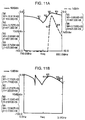
- FIG. 11 shows characteristics of the band-stop filter configured by three resonators which are disposed on a piezoelectric substrate made of LiTaO3 (lithium tantalate) using conventional circuit structure.
- FIG. 12 shows an equivalent circuit diagram of the SAW resonant element shown in FIG. 10.
- reference number 111 is a parallel capacitor C0
- reference number 112 an equivalent series inductor L1
- reference number 113 an equivalent series capacitor C1
- reference number 114 an equivalent series resistor R1.
- An object of the present invention is to attain a SAW filter which can set attenuation characteristics and pass characteristics arbitrarily.
- the SAW filter of the present invention comprises comb-shaped electrodes facing each other disposed on the same piezoelectric substrate, at least two resonators with an input and output terminals, and an equivalent transmission line which is connected between an output terminal of the first resonator and an input terminal of a second resonator.
- the phase of the transmission line can be adjusted from 5 degrees to 175 degrees arbitrarily at the series resonance frequency of the resonators.
- the band-stop filter or the band-pass filter based on the present invention can set the attenuation characteristics and the pass characteristics arbitrarily.
- a surface acoustic wave (SAW) filter of the present invention comprises, at least two resonators each having comb-shaped electrodes facing each other disposed on the same piezoelectric substrate an input terminal, output terminal, and an equivalent transmission line connected between an output terminal of a first resonator and an input terminal of a second resonator, to form a band-stop filter.
- the phase of the transmission line can be adjusted from 5 degrees to 175 degrees arbitrarily at the series resonance frequency of the resonators.
- the present invention allows the band-stop filter to be provided with fairly arbitrarily attenuation and pass characteristics.
- a SAW filter of the present invention comprises at least two resonators, each having comb-shaped electrodes facing each other disposed on the same piezoelectric substrate, an input terminal and an output terminal, each output terminal of the resonators grounded, and an equivalent transmission line connected between input terminals of the resonators, to form a stop-band filter.
- the phase of the transmission line can be adjusted from 5 degrees to 175 degrees arbitrarily at the parallel resonance frequency of the resonators.
- the present invention allows the stop-band filter to be provided with fairly arbitrarily attenuation and pass characteristics.
- an output terminal of a first resonator with comb-shaped electrodes facing each other disposed on the same piezoelectric substrate and with an input terminal and an output terminal is coupled to an input terminal of a second resonator with comb-shaped electrodes facing each other disposed on the piezoelectric substrate and with an input terminal and an output terminal
- an output terminal of a third resonator with comb-shaped electrodes facing each other disposed on the piezoelectric substrate and with an input terminal and an output terminal is coupled to an input terminal of a forth resonator with comb-shaped electrodes facing each other disposed on the piezoelectric substrate and with an input terminal and an output terminal
- an equivalent transmission line is coupled between a node between the first resonator and the second resonator and a node between the third resonator and the fourth resonator, to form a passband filter.
- the phase of the transmission line can be adjusted from 5 degrees to 175 degrees arbitrarily at the series resonance frequency of the first or third resonator or at the series resonance frequency of the second or fourth resonator.
- the present invention allows the band-pass filter to be provided with arbitrary attenuation and pass characteristics at a certain degree.
- an output terminal of a first resonator with comb-shaped electrodes facing each other disposed on the same piezoelectric substrate and with an input terminal and an output terminal is coupled to an input terminal of a second resonator with comb-shaped electrodes facing each other disposed on the piezoelectric substrate and with an input terminal and an output terminal
- an output terminal of a third resonator with comb-shaped electrodes facing each other disposed on the piezoelectric substrate and with an input terminal and an output terminal is coupled to an input terminal of a forth resonator with comb-shaped electrodes facing each other disposed on the piezoelectric substrate and with an input terminal and an output terminal
- an equivalent transmission line is coupled between a node between the first resonator and the second resonator and an input terminal of the third resonator, to form a band-pass filter.
- the phase of the transmission line can be adjusted from 5 degrees to 175 degrees arbitrarily at the series resonance frequency of the first or third resonator or at the parallel resonance frequency of the second or fourth resonator.
- the present invention allows the pass-band filter to be provided with arbitrary attenuation and the pass characteristics at a certain degree.
- the transmission line comprises ⁇ -type or T-type circuit connecting a capacitor in shunt-arm and an inductor in series-arm, to form a filter.
- the present invention allows the filter to reject undesired signal with a frequency higher than two times passband frequency.
- the transmission line comprises ⁇ -type or T-type circuit connecting an inductor in shunt-arm and a capacitor in series-arm, to form a filter.
- the present invention allows the filter to reject undesired signal with a frequency lower than a half passband frequency.
- transmission lines of some of the filter circuits have ⁇ -type or T-type circuit connecting a capacitor in shunt-arm and an inductor in series-arm and the transmission lines of the other filter circuits have ⁇ -type or T-type circuit connecting an inductor in shunt-arm and a capacitor in series-arm, to form a filter.
- the present invention allows the filter to reject undesired signal with a frequency higher than about two times the passband frequency and lower than about a half the passband frequency.
- each of the transmission lines includes one of the following elements: a capacitor with an inductor coupled in series connected in the shunt-arm so as for the series combined impedance to be the same value in the passband; a capacitor with an inductor coupled in parallel connected in the series-arm so as for the parallel combined admittance to be the same value in the passband; a inductor with a capacitor coupled in series connected in the shunt-arm so as for the series combined impedance to be the same value in the passband; or an inductor with a capacitor coupled in parallel connected in the series-arm so as for the parallel combined admittance to be the same value in the passband, to form a filter.
- This structure allows the filter to have an attenuation pole outside the band and to remove undesired signals efficiently.
- a SAW filter of the present invention comprises an equivalent transmission line configured in a multilayered body of dielectric material with relative dielectric constant less than ten (10) to form a filter, wherein the multilayered body is used as a part of an airtight seal material for the piezoelectric substrate.
- the present invention allows the SAW filter to be small size and low cost.
- the transmission line is made of silver or copper paste printed as main circuit material to form a filter.
- the present invention allows the SAW filter to have low loss.
- FIG. 1 and FIG. 2 show a circuit diagram and electrical characteristics of a SAW filter respectively, in accordance with a first exemplary embodiment of the present invention.
- FIG. 1 shows SAW resonant elements 11, 12, 13 which are disposed on one piezoelectric substrate, transmission lines 14a, 14b, input terminal 16, and output terminal 17.
- the piezoelectric substrate in this embodiment is made of lithium tantalate.
- SAW resonator 11 produces a series resonance at an attenuation frequency with zero ohms and a node between SAW resonator 11 and transmission line 14a is grounded. If an electric length of transmission line 14a is 90 degrees, an impedance measured from the opposite side (the side connected to SAW resonator 12) is open.
- a frequency at which SAW resonator 12 is set is about the same as that of SAW resonator 11, so that an impedance at the node between SAW resonator 12 and transmission line 14a is also a short. Therefore, there is a big difference between the two impedances of the both sides of the node between transmission line 14a and SAW resonator 12.
- a matching condition is normally satisfied. But the more deviation from the relation or the more mismatching allows the circuit to generate the more attenuation as pass characteristics. Therefore, the same effect is expected from connecting a transmission line between two SAW resonators.
- FIG. 2 shows that when the characteristic impedance and the line length for transmission lines 14a and 15a are 50 ohms/68 degrees and 50 ohms/55 degrees respectively in the circuit, the filter characteristics of the circuit is the loss 1.9 dB and the attenuation 33 dB in the passband. This means good characteristics.
- the filter of the present invention comprises transmission lines 14a, 15a and SAW resonators 11, 12 and 13 as an example.
- the transmission line operating as an impedance exchange element allows the filter to get good filter characteristics.
- the transmission line remarkably operates as an impedance exchange element in the electric length range from 5 to 175 degrees, but does not operate at all at zero and 180 degrees.
- FIG. 3 and FIG. 4 show a circuit diagram and electrical characteristics of a SAW filter respectively, in accordance with the second exemplary embodiment of the present invention.
- the figure shows circuit elements 31 to 35 which operate in the electrically equivalent manner to transmission lines 14a and 15a explained in FIG. 1, wherein the circuit structure of the embodiment is a low-pass ⁇ -type filter connecting a capacitor in shunt-arm and an inductor in series-arm.
- FIG. 4 shows that the filter characteristics of the circuit is nearly as good as that of the first embodiment in the vicinity of the passband and larger attenuation than 40 dB in high frequency range. The reason is that finally the transmission lines of the present invention are equivalently converted into five concentrated constant elements, and the frequency characteristics of the impedances of the concentrated constant elements gets attenuation characteristics in high frequency range.
- the elements used in ⁇ -type connection for the transmission line and in addition the elements allow the filter of the invention to have large attenuation characteristics especially in far high frequency range.
- the same effect is expected from a T-type circuit structure or a circuit structure of a high-pass T-type filter connecting an inductor in shunt-arm and a capacitor in series-arm, and the circuit structures allow the filter of the invention to have large attenuation characteristics especially in far low frequency range.
- FIG. 5 and FIG. 6 show a circuit diagram and electrical characteristics of a SAW filter respectively, in accordance with the third exemplary embodiment of the present invention.
- the figure shows SAW resonant elements 51, 52, 53 which are disposed on one piezoelectric substrate, transmission lines 54, 55, input terminal 16, and output terminal 17.
- the piezoelectric substrate in this embodiment is lithium tantalate.
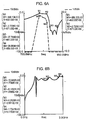
- FIG. 6 shows that when the characteristic impedance and the line length at the center frequency of the passband for transmission lines 54 and 55 are 66 ohms/79 degrees and 38 ohms/142 respectively in the circuit the filter characteristics of the circuit is the loss 2.7 dB, the attenuation 38 dB in thepassband. This means good characteristics.
- the filter of the present invention comprises transmission lines 54, 55 and SAW resonators 51 to 53 as an example.
- the transmission line operating as an impedance exchange element allows the filter to get good filter characteristics.
- the transmission line remarkably operates as an impedance exchange element in the electric length range from 5 to 175 degrees, but does not operate at all at zero and 180 degrees.
- the filter of this embodiment is designed to set the series resonance point of the SAW resonators within the passband and the parallel resonance point of the SAW resonators within the attenuation band, so that the series resonance point of the SAW resonators must be lower than the parallel resonance point, therefore on the contrary to the first embodiment, the filter is especially effective for a case that attenuation is mainly required in frequency range over the passband.
- FIG. 7 and FIG. 8 show a circuit diagram and electrical characteristics of a SAW filter respectively, in accordance with the fourth exemplary embodiment of the present invention.
- the figure shows SAW resonant elements 71 to 76 which are disposed on one piezoelectric substrate, transmission lines 77, 78, input terminal 16, and output terminal 17.
- the piezoelectric substrate in this embodiment is lithium tantalate.
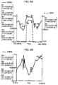
- FIG. 8 shows that when the characteristics impedance and the line length at the center frequency of the passband for transmission lines 77 and 78 are 43 ohms/102 degrees and 67 ohms/81 respectively in the circuit, the filter characteristics of the circuit is the loss 2.7 dB, the attenuation 35 dB in thepassband. This means good bandpass characteristics.
- the filter of the present invention comprises transmission lines 77, 78 and SAW resonator 71 to 76 as an example.
- the transmission line operating as an impedance exchange element allows the filter to get good filter characteristics.
- the transmission line remarkably operates as an impedance exchange element in the electric length range from 5 to 175 degrees, but does not operate at all at zero and 180 degrees.
- the design concept for the filter of this embodiment is for the filter to configure a resonator group formed in ladder-type e.g. SAW resonators 71and 72 as a unit and to get attenuation characteristics in frequency range under the passband with SAW resonators 71, 73, and 75 and attenuation characteristics in frequency range over the passband with SAW resonators 72, 74, and 76
- the same effect is expected from the filter using ⁇ -type or T-type equivalent circuit with capacitors and inductors for low-pass or high-pass characteristics. Then this embodiment allows the filter of the invention to have attenuation characteristics in a frequency range fairly far away from the passband.
- this embodiment configuring one of the transmission lines as a high-pass type and theother as a low-pass type allows the filter to get characteristics combining broad band-pass filters and to reject undesired signal far from the band efficiently. Namely, this embodiment allows the filter of the present invention to get attenuation in a frequency range where SAW resonators only by themselves cannot attain the attenuation, while some conventional configurations specially need other filters to attain the attenuation. But the configuration of the present invention does not need such filters.
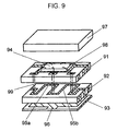
- FIG. 9 shows an exploded isometric drawing of blocks of a SAW filter, in accordance with the fifth exemplary embodiment of the present invention.
- the figure shows multilayered bodies 91 to 93 of dielectric sheets, piezoelectric substrate 94, transmission lines 95aand 95b formed by printing on multilayered body 92, shield electrode 96 formed by printing the same way, and cap 97 covering piezoelectric substrate 94.
- this embodiment is a tangible form into which a circuit shown in FIG. 1 is put, where the SAW resonators formed on piezoelectric substrate 94 and transmission lines 95a and 95b are connected each other by via holes 99.
- Designated values of characteristic impedance and electric length of transmission lines 95a and 95b are attained by width of the lines and clearance from upper/under grounding electrodes, or thickness of dielectric sheets 91and 92 and physical length of the printed material.
- the filter having a shield electrode disposed at the bottom makes the characteristic impedance stabilized. Therefore, it is better that the filter has the shield electrode so as well to reject an influence from some external element e.g. a pattern of a mother substrate.
- the configuration described above allows a SAW filter to be more miniaturized and higher reliable. And for example, a filter for cellular phone is estimated a few millimeters long. If the filter has strip line type transmission lines of tri-plate structure with multilayered body about one millimeter wide and 0.1 millimeter thick and the characteristic impedance is about 50 ohms, appropriate value of relative dielectric constant for the multilayered body is less than about ten (10).
- the dielectric materials are for example aluminum oxide, foresterite, and glass ceramic. Using silver, copper, or metallic material including high percentage of those metals allows the filter to have low loss.
- the present invention configures a filter comprising transmission lines operating as impedance exchange elements or bulk element circuits into which the transmission lines are equivalently converted and SAW resonators. Therefore, the filter attains large attenuation with a few stages. As a result, the present invention can configure a filter having band-stop or band-pass filter with large attenuation and low insertion loss characteristics.
Landscapes
- Physics & Mathematics (AREA)
- Acoustics & Sound (AREA)
- Surface Acoustic Wave Elements And Circuit Networks Thereof (AREA)
Applications Claiming Priority (3)
| Application Number | Priority Date | Filing Date | Title |
|---|---|---|---|
| JP32323698 | 1998-11-13 | ||
| JP32323698 | 1998-11-13 | ||
| PCT/JP1999/006272 WO2000030252A1 (fr) | 1998-11-13 | 1999-11-11 | Filtre d'ondes acoustiques de surface |
Publications (2)
| Publication Number | Publication Date |
|---|---|
| EP1050962A1 true EP1050962A1 (fr) | 2000-11-08 |
| EP1050962A4 EP1050962A4 (fr) | 2003-05-14 |
Family
ID=18152533
Family Applications (1)
| Application Number | Title | Priority Date | Filing Date |
|---|---|---|---|
| EP99972384A Ceased EP1050962A4 (fr) | 1998-11-13 | 1999-11-11 | Filtre d'ondes acoustiques de surface |
Country Status (4)
| Country | Link |
|---|---|
| US (1) | US6404302B1 (fr) |
| EP (1) | EP1050962A4 (fr) |
| JP (1) | JP3482957B2 (fr) |
| WO (1) | WO2000030252A1 (fr) |
Cited By (4)
| Publication number | Priority date | Publication date | Assignee | Title |
|---|---|---|---|---|
| EP1398876A1 (fr) * | 2002-09-10 | 2004-03-17 | Matsushita Electric Industrial Co., Ltd. | Filtre acoustique réjecteur de bande |
| WO2006045176A1 (fr) | 2004-10-29 | 2006-05-04 | Nortel Networks Limited | Filtres coupe-bande |
| WO2007131501A1 (fr) * | 2006-05-15 | 2007-11-22 | Epcos Ag | composant électrique |
| CN1526199B (zh) * | 2001-05-14 | 2010-04-28 | 因芬尼昂技术股份公司 | 平衡和非平衡线路系统的滤波器装置 |
Families Citing this family (33)
| Publication number | Priority date | Publication date | Assignee | Title |
|---|---|---|---|---|
| JP4552389B2 (ja) * | 1998-11-13 | 2010-09-29 | パナソニック株式会社 | 弾性表面波フィルタ |
| JP2002141771A (ja) * | 2000-08-21 | 2002-05-17 | Murata Mfg Co Ltd | 弾性表面波フィルタ装置 |
| JP2003069382A (ja) * | 2001-08-27 | 2003-03-07 | Matsushita Electric Ind Co Ltd | 弾性表面波フィルタとそれを用いたアンテナ共用器 |
| US6710677B2 (en) * | 2002-02-12 | 2004-03-23 | Nortel Networks Limited | Band reject filters |
| US6879224B2 (en) * | 2002-09-12 | 2005-04-12 | Agilent Technologies, Inc. | Integrated filter and impedance matching network |
| JP2005033246A (ja) | 2003-07-07 | 2005-02-03 | Matsushita Electric Ind Co Ltd | Sawフィルタとそれを用いた電子デバイス |
| US7301420B2 (en) * | 2003-11-20 | 2007-11-27 | Matsushita Electric Industrial Co., Ltd. | Piezoelectric resonator filter |
| JP4440749B2 (ja) * | 2004-11-02 | 2010-03-24 | ローム株式会社 | 画像読み取り装置 |
| JP4626652B2 (ja) * | 2005-08-02 | 2011-02-09 | 株式会社村田製作所 | 弾性波フィルタ装置 |
| NO323325B1 (no) * | 2005-08-11 | 2007-03-19 | Norspace As | Elektronisk filter |
| JP4697229B2 (ja) * | 2005-11-01 | 2011-06-08 | 株式会社村田製作所 | 弾性波フィルタ装置 |
| CN101356730B (zh) * | 2006-02-13 | 2011-02-16 | 株式会社村田制作所 | Saw滤波器装置 |
| US7586389B2 (en) | 2006-06-19 | 2009-09-08 | Maxim Integrated Products, Inc. | Impedance transformation and filter using bulk acoustic wave technology |
| US7598827B2 (en) * | 2006-06-19 | 2009-10-06 | Maxim Integrated Products | Harmonic termination of power amplifiers using BAW filter output matching circuits |
| DE102007024895B4 (de) * | 2007-05-29 | 2015-08-27 | Epcos Ag | Multiband-Filter |
| CN101939912A (zh) * | 2008-02-05 | 2011-01-05 | 日本电波工业株式会社 | 滤波器、便携式终端和电子部件 |
| BE1019445A3 (fr) * | 2010-08-11 | 2012-07-03 | Reza Yves | Procede d'extraction d'information audio. |
| KR101919115B1 (ko) * | 2012-02-29 | 2018-11-15 | 삼성전자주식회사 | Bawr 을 이용한 필터 |
| US9203129B2 (en) * | 2012-10-01 | 2015-12-01 | Teledyne Wireless, Llc | Increasing the minimum rejection bandwidth of a YIG-tuned notch filter using a shunt YIG resonator |
| US9246533B2 (en) | 2012-10-18 | 2016-01-26 | Skyworks Panasonic Filter Solutions Japan Co., Ltd. | Electronic device including filter |
| WO2015083415A1 (fr) * | 2013-12-03 | 2015-06-11 | 株式会社村田製作所 | Dispositif de filtre |
| DE102014111901B4 (de) * | 2014-08-20 | 2019-05-23 | Snaptrack, Inc. | Duplexer |
| DE102014111904A1 (de) * | 2014-08-20 | 2016-02-25 | Epcos Ag | Abstimmbares HF-Filter mit Parallelresonatoren |
| DE102014111912B4 (de) | 2014-08-20 | 2024-06-13 | Snaptrack, Inc. | HF-Filter |
| JP6323348B2 (ja) * | 2015-01-23 | 2018-05-16 | 株式会社村田製作所 | フィルタ装置 |
| DE112016001482B4 (de) * | 2015-04-01 | 2025-05-22 | Murata Manufacturing Co., Ltd. | Duplexer |
| JP6668213B2 (ja) | 2015-10-01 | 2020-03-18 | スカイワークスフィルターソリューションズジャパン株式会社 | 分波器と通信機器 |
| US10404234B2 (en) | 2016-09-02 | 2019-09-03 | Skyworks Filter Solutions Japan Co., Ltd. | Filter device with phase compensation, and electronic devices including same |
| JP2018088678A (ja) | 2016-11-29 | 2018-06-07 | スカイワークス ソリューションズ, インコーポレイテッドSkyworks Solutions, Inc. | 位相をキャンセルするループ回路を含むフィルタ |
| GB2577361B (en) | 2018-07-18 | 2023-03-01 | Skyworks Solutions Inc | FBAR filter with integrated cancelation circuit |
| US20220029646A1 (en) * | 2020-07-27 | 2022-01-27 | Corning Research & Development Corporation | Radio frequency transceiver filter circuit having inter-stage impedance matching |
| CN112350684B (zh) * | 2020-10-29 | 2021-08-10 | 诺思(天津)微系统有限责任公司 | 一种声波滤波器、多工器、通信设备 |
| US12580550B2 (en) | 2022-12-20 | 2026-03-17 | Skyworks Solutions, Inc. | Bulk acoustic wave filter circuit having phase cancelling circuit |
Family Cites Families (14)
| Publication number | Priority date | Publication date | Assignee | Title |
|---|---|---|---|---|
| JPS437739B1 (fr) * | 1964-10-29 | 1968-03-25 | ||
| JPS432402B1 (fr) * | 1964-12-18 | 1968-01-29 | ||
| JPS51142246A (en) * | 1975-06-03 | 1976-12-07 | Pioneer Electronic Corp | Filter network |
| JPS61193501A (ja) * | 1985-02-21 | 1986-08-28 | Murata Mfg Co Ltd | フイルタ |
| JPH1093376A (ja) * | 1991-10-28 | 1998-04-10 | Fujitsu Ltd | 弾性表面波フィルタ |
| JP3434853B2 (ja) * | 1993-06-28 | 2003-08-11 | 株式会社リコー | モデムの制御方法 |
| JPH0722892A (ja) * | 1993-07-05 | 1995-01-24 | Murata Mfg Co Ltd | Sawフィルタ |
| JPH07231241A (ja) * | 1994-02-17 | 1995-08-29 | Hitachi Ltd | 弾性表面波装置 |
| JPH07263995A (ja) * | 1994-03-22 | 1995-10-13 | Hitachi Ltd | 弾性表面波装置およびそれを用いたアンテナ分波器 |
| US5499002A (en) * | 1994-04-28 | 1996-03-12 | Kinsman; Robert G. | Resonator filter utilizing cascaded impedance inverters |
| JPH1013187A (ja) | 1996-06-19 | 1998-01-16 | Oki Electric Ind Co Ltd | はしご型フィルタ |
| JPH1065489A (ja) * | 1996-08-13 | 1998-03-06 | Hitachi Ltd | 弾性表面波素子を用いたフィルタおよび該フィルタを用いたアンテナ分波器 |
| DE69738934D1 (de) * | 1997-02-12 | 2008-10-02 | Oki Electric Ind Co Ltd | Akustische Oberflächenwellenfilter mit durch Impedanzschaltungen erzeugten Dämpfungspolen |
| JP3525408B2 (ja) | 1998-05-07 | 2004-05-10 | 富士通株式会社 | 分波器パッケージ |
-
1999
- 1999-11-11 EP EP99972384A patent/EP1050962A4/fr not_active Ceased
- 1999-11-11 WO PCT/JP1999/006272 patent/WO2000030252A1/fr not_active Ceased
- 1999-11-11 US US09/600,233 patent/US6404302B1/en not_active Expired - Lifetime
- 1999-11-11 JP JP2000583159A patent/JP3482957B2/ja not_active Expired - Lifetime
Non-Patent Citations (2)
| Title |
|---|
| See also references of WO0030252A1 * |
| TAGAMI T ET AL: "RESONATOR TYPE SAW FILTER" OKI TECHNICAL REVIEW, OKI ELECTRIC INDUSTRY, TOKYO, JP, vol. 63, no. 158, 1 April 1997 (1997-04-01), pages 59-64, XP000699796 ISSN: 0912-5566 * |
Cited By (10)
| Publication number | Priority date | Publication date | Assignee | Title |
|---|---|---|---|---|
| CN1526199B (zh) * | 2001-05-14 | 2010-04-28 | 因芬尼昂技术股份公司 | 平衡和非平衡线路系统的滤波器装置 |
| EP1398876A1 (fr) * | 2002-09-10 | 2004-03-17 | Matsushita Electric Industrial Co., Ltd. | Filtre acoustique réjecteur de bande |
| US7084718B2 (en) | 2002-09-10 | 2006-08-01 | Matsushita Electric Industrial Co., Ltd. | Band elimination filter, filter device, antenna duplexer and communication apparatus |
| WO2006045176A1 (fr) | 2004-10-29 | 2006-05-04 | Nortel Networks Limited | Filtres coupe-bande |
| EP1807933A4 (fr) * | 2004-10-29 | 2009-06-10 | Nortel Networks Ltd | Filtres coupe-bande |
| US7777597B2 (en) | 2004-10-29 | 2010-08-17 | Nortel Networks Limited | Band reject filters |
| US8004371B2 (en) | 2004-10-29 | 2011-08-23 | Nortel Networks Limited | Band reject filters |
| US8207799B2 (en) | 2004-10-29 | 2012-06-26 | Rockstar Bidco, LP | Band reject filters |
| WO2007131501A1 (fr) * | 2006-05-15 | 2007-11-22 | Epcos Ag | composant électrique |
| US7821358B2 (en) | 2006-05-15 | 2010-10-26 | Epcos Ag | Electrical component |
Also Published As
| Publication number | Publication date |
|---|---|
| WO2000030252A1 (fr) | 2000-05-25 |
| JP3482957B2 (ja) | 2004-01-06 |
| EP1050962A4 (fr) | 2003-05-14 |
| US6404302B1 (en) | 2002-06-11 |
Similar Documents
| Publication | Publication Date | Title |
|---|---|---|
| US6404302B1 (en) | Surface acoustic wave filter utilizing a transmission line with phase characteristics that increase filter out of band attenuation | |
| JP4000960B2 (ja) | 分波器、通信装置 | |
| JPWO2000030252A1 (ja) | 弾性表面波フィルタ | |
| US8179211B2 (en) | RF-filter with improved adjacent channel suppression | |
| JP3849289B2 (ja) | 弾性表面波装置 | |
| CN112737544B (zh) | 声表面波滤波器 | |
| EP0898363B1 (fr) | Dispositif à ondes acoustiques de surface | |
| CN107026634A (zh) | 带通滤波器以及双工器 | |
| US4785270A (en) | Monolithic lattice saw filter | |
| US20200106419A1 (en) | Electro-acoustic rf filter with increased flank steepness, multiplexer and method of designing an electro-acoustic rf filter | |
| US6882250B2 (en) | High-frequency device and communication apparatus | |
| JPH1065489A (ja) | 弾性表面波素子を用いたフィルタおよび該フィルタを用いたアンテナ分波器 | |
| WO2005004327A1 (fr) | Filtre a ondes de surface et dispositif utilisant un tel filtre | |
| CN100477519C (zh) | 表面声波滤波器 | |
| JPH0832402A (ja) | 弾性表面波装置、移動無線機用分波器および移動無線装置 | |
| JPH10163708A (ja) | 有極型誘電体フィルタ及びこれを用いた誘電体デュプレクサ | |
| JP3729185B2 (ja) | 弾性表面波フィルタ | |
| JPH10308607A (ja) | 誘電体デュプレクサ装置 | |
| JP4552389B2 (ja) | 弾性表面波フィルタ | |
| JP2003332882A (ja) | 弾性表面波フィルタ | |
| US12362727B2 (en) | Composite filter device | |
| KR100613649B1 (ko) | 광대역 체적탄성파 여파기 모듈 | |
| JPH1056304A (ja) | 分波器 | |
| KR20070040516A (ko) | 쏘 듀플렉서 | |
| JPH11225034A (ja) | 積層型バンドパスフィルタ |
Legal Events
| Date | Code | Title | Description |
|---|---|---|---|
| PUAI | Public reference made under article 153(3) epc to a published international application that has entered the european phase |
Free format text: ORIGINAL CODE: 0009012 |
|
| 17P | Request for examination filed |
Effective date: 20000718 |
|
| AK | Designated contracting states |
Kind code of ref document: A1 Designated state(s): AT BE CH CY DE DK ES FI FR GB GR IE IT LI LU MC NL PT SE |
|
| A4 | Supplementary search report drawn up and despatched |
Effective date: 20030327 |
|
| RBV | Designated contracting states (corrected) |
Designated state(s): DE FR GB |
|
| 17Q | First examination report despatched |
Effective date: 20070830 |
|
| STAA | Information on the status of an ep patent application or granted ep patent |
Free format text: STATUS: THE APPLICATION HAS BEEN REFUSED |
|
| 18R | Application refused |
Effective date: 20080414 |