EP1051004A2 - Empfänger und Verfahren zum Empfangen eines FSK-Signal - Google Patents
Empfänger und Verfahren zum Empfangen eines FSK-Signal Download PDFInfo
- Publication number
- EP1051004A2 EP1051004A2 EP00115544A EP00115544A EP1051004A2 EP 1051004 A2 EP1051004 A2 EP 1051004A2 EP 00115544 A EP00115544 A EP 00115544A EP 00115544 A EP00115544 A EP 00115544A EP 1051004 A2 EP1051004 A2 EP 1051004A2
- Authority
- EP
- European Patent Office
- Prior art keywords
- signal
- fsk
- zero crossing
- zero
- binary
- Prior art date
- Legal status (The legal status is an assumption and is not a legal conclusion. Google has not performed a legal analysis and makes no representation as to the accuracy of the status listed.)
- Withdrawn
Links
Images


Classifications
-
- H—ELECTRICITY
- H04—ELECTRIC COMMUNICATION TECHNIQUE
- H04L—TRANSMISSION OF DIGITAL INFORMATION, e.g. TELEGRAPHIC COMMUNICATION
- H04L27/00—Modulated-carrier systems
- H04L27/10—Frequency-modulated carrier systems, i.e. using frequency-shift keying
- H04L27/14—Demodulator circuits; Receiver circuits
- H04L27/156—Demodulator circuits; Receiver circuits with demodulation using temporal properties of the received signal, e.g. detecting pulse width
- H04L27/1563—Demodulator circuits; Receiver circuits with demodulation using temporal properties of the received signal, e.g. detecting pulse width using transition or level detection
-
- H—ELECTRICITY
- H04—ELECTRIC COMMUNICATION TECHNIQUE
- H04L—TRANSMISSION OF DIGITAL INFORMATION, e.g. TELEGRAPHIC COMMUNICATION
- H04L27/00—Modulated-carrier systems
- H04L27/10—Frequency-modulated carrier systems, i.e. using frequency-shift keying
- H04L27/12—Modulator circuits; Transmitter circuits
- H04L27/122—Modulator circuits; Transmitter circuits using digital generation of carrier signals
Definitions
- This invention relates to transmitting and receiving frequency-shift keyed (FSK) signals, and in particular to digital FSK transmitters, receivers and methods of recovering baseband signals from FSK signals.
- FSK frequency-shift keyed
- Frequency-shift keying is a form of frequency modulation used especially in telegraphic and facsimile transmission.
- the modulating wave in frequency-shift keying shifts the output frequency between predetermined values corresponding to the frequencies of correlated sources.
- a digital phase locked loop which can be used as a component of an FSK receiver is also known, but this circuit requires the use of an analog filter to operate as an FSK receiver. Also, in order to implement a digital FSK receiver according to known techniques, it is necessary to use a mixed-mode ASIC (application specific integrated circuit) which is both expensive and requires a comparatively long development time.
- PLL phase locked loop
- a digital FSK receiver for receiving an FSK signal containing at least two different signal frequencies, the receiver comprising:
- a method of recovering a baseband signal from an FSK signal having at least two different signal frequencies comprising:
- an FSK transmitter for transmitting an FSK signal containing at least two different signal frequencies; the transmitter comprising:
- a preferred embodiment of this invention provides a digital FSK transmitter receiver which utilises information contained in the zero crossings of the received FSK signal.
- the FSK signal is transmitted by a dual register preprogrammed to add a predetermined count to an accumulator through an adder to generate the exact dual FSK frequencies required.
- the same clock signal used for the accumulator is also used as a signal for the dual registers by way of the signal going to a single stage shift register.
- the zero crossings of the transmitted FSK signals are converted to a digital format by counting the number of clock pulses between successive zero crossings.
- a second clock is used to insert the last zero crossing count into a multistage first in-first out (FIFO) buffer.
- An accumulator stores the sum of the values in the FIFO.
- a threshold is established whereby any value in the accumulator below the threshold is considered a zero and any value above is considered a one.
- the accumulator and the FIFO serve as a "digital" filter. If a zero crossing is received early (or late) as a result of noise, the value in the accumulator will decrease (or increase). However, if the next zero crossing is not displaced, it will bring the accumulator back to its expected value.
- the preferred digital FSK transmitter receiver has several advantages over known analog FSK receivers.
- the digital FSK receiver allows the use of a gate array rather than a mixed-mode ASIC.
- a gate array implementation is cheaper to develop, requires less turn-around time, and reduces the part per price to less than half that of a mixed-mode ASIC.
- the digital FSK receiver also does not require a filter which is necessary in analog FSK receivers. This can reduce the board area required for the equipment by up to a factor of two. Where it is required to provide both a transmitter and a receiver, the two circuits can share a number of components, including an adder and an accumulator.
- the present invention further provides a digital FSK receiver for receiving an FSK signal containing at least two different signal frequencies, the receiver comprising: a zero crossing detector for detecting zero crossings of the FSK signal; interval measuring means connected to the zero crossing detector for measuring the intervals between the zero crossings; a buffer for storing a number of previous zero crossing values; an accumulator for maintaining the sum of the stored zero crossing values (with a possible fixed offset); and a binary output means for outputting a one or a zero depending on whether the value in the accumulator is above or below a selected threshold.
- a digital FSK transmitter illustrated in Figure 1 comprises a thirteen stage accumulator, a thirteen stage binary adder, and means for adding a number to the accumulator at a 3 MHz rate as determined by the CLOCK used for the accumulator, the adding means being constituted by two registers (register one and register two) and a register select circuit.
- the half period of the frequency generated must be a multiple of 333 + n seconds (the period is the reciprocal of the frequency).
- the best that can be done in generating these desired frequencies is to divide the 3 MHz generated by the clock by the divisors 158 and 98, giving 18.987 KHz and 30.612 KHz respectively.
- the accumulator maximum value should be divisible by both 158 and 198. The largest number, less than 8192, which is divisible by both 158 and 98 is 7742. This number is 450 short of the full accumulation value of 8192.
- a DATA IN signal to the register select circuit is binary in nature (0, 1) and corresponds to the frequency desired from the output FSK OUT of the accumulator.
- the register select circuit thus enables only the register one for an input signal of "1” and enables only the register two for an input signal of "0".
- the enabled register is thus activated to pass either of the two numbers stored therein to the binary adder.
- the register one has the numbers 49 and 274 stored therein while the register two has the numbers 79 and 304 stored therein.
- the enabled register will transmit either the higher or lower of the two numbers depending on whether it receives a HI or LO signal on a HI/LO input line.
- the HI/LO signal is derived from the output of an AND gate having inputs derived from the output of the 12th stage of the accumulator and an output Q of a single stage shift register which has an input D from the 12th stage of the accumulator and is clocked by the 3 MHz CLOCK.
- the output Q of the shift register is the accumulator 12th stage delayed by one clock cycle of the 3 MHz clock input CLK.
- the LO numbers transmitted from the registers are due to the inputs to the AND gate being opposite in sign except when the 12th stage of the accumulator changes from a "0" to a "1" indicating the need for adding the previously-mentioned number 225 which is then added to the next normally transmitted number, either 49 or 79, to make for a single transmission of either 274 or 304 from the 13th stage of the accumulator depending on whether the register one or the register two of the accumulator is enabled.
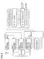
- Figure 2 illustrates a digital FSK receiver embodying the present invention. It has been designed so as to use much of the circuitry in the FSK transmitter shown in Figure 1.
- intervals between zero crossings are converted to numbers by counting the pulses of a clock, labelled ZCLOCK, in a (zero crossing) counter. At each zero crossing, the count resulting from the previous interval is stored in a (zero crossing) register.
- the value of the register is inserted in a 16 deep, 8 bit wide FIFO (first in-first out) buffer.
- An accumulator stores the sum of the values in the FIFO (plus a fixed offset). Rather than sum the 16 values each time, the accumulator is kept current by subtracting the oldest value in the FIFO from the new value being inserted and adding the resultant to the accumulator.
- the received signal FSK IN were a continuous "zero” (30.5 KHz), it would have zero crossing intervals of 16.393 microseconds. A continuous "one” (19 KHz) would have zero crossing intervals of 26.316 microseconds. With a ZCLOCK of 6 MHz, these intervals would yield counts of 98 and 158 respectively. Thus a continuous "0" input would give a value for the sum of the FIFO of 1568 and a continuous "1" input would give a value of 2528. The mid-point is 2048, or 2**11th. As seen in Figure 2, the baseband output RCVNR2 is the 12th stage of the accumulator (a "one" in the 12th stage has a value of 2**11th).
- the SCLOCK is 250 KHz and, because the 13 bit adder is relatively slow, it is not practical to subtract the old value of the buffer between successive SCLOCKs. Instead, an 8 bit adder calculates the difference between the new and the old values of the FIFO and this result is added to the accumulator at the SCLOCK rate. It is important to note that the result to be added to the accumulator may be positive or negative. A negative number from the 8 bit adder is automatically expressed in two's complement form, and so adding it to the accumulator will give the correct result.
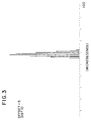
- the receiver embodying the present invention has been simulated using several BASIC programs. Calculations were performed to determine the spacings of zero crossings which would result from a perfect FSK transmitter being modulated by an input data stream. Delays were investigated for "one" to “zero” transitions and for "zero” to “one” transitions and the phase of the input data stream to the FSK signal was varied over all the possible values in increments of one microsecond.
- a third program was run to simulate the response of the circuit to a random input.
- the plot of the accumulator value compared to the input waveform is shown in Figure 5.
- the solid line waveform is the data input to an FSK transmitter.
- the "ones” and “zeroes” below the waveform show the data to be transmitted to a distant receiver.
- the dotted line waveform is the value in the accumulator of the distant receiver. As can be seen in Figure 5, the dotted line waveform has a number of changes in slope which will be described in more detail below.
- the upper flat portions of the dotted line waveform indicate that the FIFO contains 16 values of 158.
- the lower flat portions of the dotted line waveform indicate that the FIFO contains 16 values of 98.
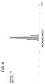
- the slopes which connect the upper and lower portions are a function of when the change from a "one" to a "zero” or a "zero" to a "one” has occurred. If the data transition occurs at a zero crossing there will be a single slope. If the transition occurs between zero crossings, an intermediate count will be stored in the FIFO and three different slopes will occur as shown at slopes A, which are at a transition between a received "one” and a received "zero", in the dotted line waveform. An enlargement of the slopes A is shown in Figure 5A.
- a slope 1 of A occurs because 158 is being shifted out of the FIFO but a value less than 158 (and greater than 98) is being shifted in.
- a slope 2 occurs because 98 is being shifted into the FIFO and 158 is being shifted out.
- a slope 3 occurs when the intermediate values are shifted out of the FIFO and 98 is being shifted in.
- Figure 7 shows the actual results achieved in a gate array chip constructed according to the present technique.
- Figure 7 illustrates the delay between a transmitted signal CH1 and a received signal CH2.
- 0 : 0 0 0 0 0 5 0 0 0 0 0 10 : 0 0 0 0 0 15 : 0 0 0 0 0 20 : 0 0 0 0 25 : 0 0 0 0 0 30 : 0 0 0 0 0 0 35 : 0 0 0 0 40 : 0 0 0 0 0 45 : 0 0 0 0 50 : 0 0 0 0 37 55 : 111 188 264 240 166 60 : 88 13 0 0 0 65 : 0 0 0 0 0 70 : 0 0 0 0 0 75 : 0 0 0 0 0 80 : 0 0 0
Landscapes
- Engineering & Computer Science (AREA)
- Computer Networks & Wireless Communication (AREA)
- Signal Processing (AREA)
- Digital Transmission Methods That Use Modulated Carrier Waves (AREA)
Applications Claiming Priority (3)
| Application Number | Priority Date | Filing Date | Title |
|---|---|---|---|
| US07/752,758 US5311556A (en) | 1991-08-30 | 1991-08-30 | Digital FSK transmitter receiver and method of operating same |
| US752758 | 1991-08-30 | ||
| EP19920307693 EP0529986A3 (en) | 1991-08-30 | 1992-08-24 | Fsk modulator and demodulator |
Related Parent Applications (1)
| Application Number | Title | Priority Date | Filing Date |
|---|---|---|---|
| EP19920307693 Division EP0529986A3 (en) | 1991-08-30 | 1992-08-24 | Fsk modulator and demodulator |
Publications (2)
| Publication Number | Publication Date |
|---|---|
| EP1051004A2 true EP1051004A2 (de) | 2000-11-08 |
| EP1051004A3 EP1051004A3 (de) | 2001-01-10 |
Family
ID=25027711
Family Applications (2)
| Application Number | Title | Priority Date | Filing Date |
|---|---|---|---|
| EP00115544A Withdrawn EP1051004A3 (de) | 1991-08-30 | 1992-08-24 | Empfänger und Verfahren zum Empfangen eines FSK-Signal |
| EP19920307693 Ceased EP0529986A3 (en) | 1991-08-30 | 1992-08-24 | Fsk modulator and demodulator |
Family Applications After (1)
| Application Number | Title | Priority Date | Filing Date |
|---|---|---|---|
| EP19920307693 Ceased EP0529986A3 (en) | 1991-08-30 | 1992-08-24 | Fsk modulator and demodulator |
Country Status (7)
| Country | Link |
|---|---|
| US (2) | US5311556A (de) |
| EP (2) | EP1051004A3 (de) |
| JP (1) | JPH05284181A (de) |
| AU (2) | AU653053B2 (de) |
| BR (1) | BR9203324A (de) |
| CA (1) | CA2077227C (de) |
| MX (1) | MX9204989A (de) |
Cited By (1)
| Publication number | Priority date | Publication date | Assignee | Title |
|---|---|---|---|---|
| US7646827B2 (en) * | 2002-04-02 | 2010-01-12 | Infineon Technologies Ag | Demodulation of a digitally frequency-modulated analog received signal by evaluation of the time intervals between the zero crossings |
Families Citing this family (22)
| Publication number | Priority date | Publication date | Assignee | Title |
|---|---|---|---|---|
| CA2116042C (en) * | 1994-02-21 | 1999-03-23 | Alexander F. Tulai | Digital fsk receiver using double zero-crossing |
| US5513219A (en) * | 1994-08-26 | 1996-04-30 | Compaq Computer Corporation | Apparatus and method for transmitting information with a subminimally modulated transmission signal |
| FR2738423B1 (fr) * | 1995-08-30 | 1997-09-26 | Snecma | Demodulateur de frequence numerique |
| US5712878A (en) * | 1996-08-19 | 1998-01-27 | Elsag International N.V. | Digital FSK modulator |
| KR100186753B1 (ko) * | 1996-08-24 | 1999-05-15 | 삼성전자주식회사 | 직접 변복조 방식이 적용된 디지탈 무선 송수신 시스템 |
| US6144253A (en) * | 1997-10-27 | 2000-11-07 | Elsag International N.V. | Digital FSK demodulator |
| US6272184B1 (en) * | 1997-12-17 | 2001-08-07 | Conexant Systems, Inc. | Non-coherent frequency shift keying detection scheme |
| FR2784256B1 (fr) * | 1998-10-02 | 2002-12-06 | Faure Res | Demodulateur numerique, et son procede de demodulation d'un signal module par deplacement de frequence |
| FR2811170A1 (fr) * | 2000-07-03 | 2002-01-04 | Valeo Electronique | Pilote d'antenne emettrice d'un signal bi-frequence a commutation de frequence synchronisee |
| FR2819970B1 (fr) * | 2001-01-23 | 2003-02-28 | Sagem | Procede de mise en service et d'utilisation d'une liaison bidirectionnelle de donnees et modem pour la mise en oeuvre du procede |
| US6990157B2 (en) * | 2001-02-24 | 2006-01-24 | Texas Instruments Incorporated | All-digital FSK demodulation with selectable data rate and adjustable resolution |
| US6385276B1 (en) | 2001-06-12 | 2002-05-07 | Rf Micro Devices, Inc. | Dual-modulus prescaler |
| US6693468B2 (en) | 2001-06-12 | 2004-02-17 | Rf Micro Devices, Inc. | Fractional-N synthesizer with improved noise performance |
| US7003049B2 (en) * | 2001-06-12 | 2006-02-21 | Rf Micro Devices, Inc. | Fractional-N digital modulation with analog IQ interface |
| US6448831B1 (en) | 2001-06-12 | 2002-09-10 | Rf Micro Devices, Inc. | True single-phase flip-flop |
| US6779010B2 (en) | 2001-06-12 | 2004-08-17 | Rf Micro Devices, Inc. | Accumulator with programmable full-scale range |
| US6891905B1 (en) | 2001-08-23 | 2005-05-10 | National Semiconductor Corporation | Apparatus and method for FSK demodulation with integrated time and frequency tracking |
| DE10342193B3 (de) * | 2003-09-12 | 2005-04-07 | Infineon Technologies Ag | Verfahren zur Rekonstruktion von Nulldurchgangsinformation von verrauschten winkelmodulierten Signalen nach einer Limiter-Diskriminator-Signalverarbeitung |
| US7292637B2 (en) * | 2003-12-17 | 2007-11-06 | Rambus Inc. | Noise-tolerant signaling schemes supporting simplified timing and data recovery |
| EP2225862B1 (de) * | 2007-12-28 | 2018-11-07 | Spectrum Controls, Inc. | Mikrosteuerung mit fsk-modem |
| US8373357B2 (en) * | 2009-01-26 | 2013-02-12 | Microchip Technology Incorporated | Modulator module in an integrated circuit device |
| IT201600111351A1 (it) * | 2016-11-04 | 2018-05-04 | St Microelectronics Des & Appl | Procedimento per rivelare segnali con modulazione fsk, circuito, dispositivo e prodotto informatico corrispondenti |
Family Cites Families (13)
| Publication number | Priority date | Publication date | Assignee | Title |
|---|---|---|---|---|
| US3597599A (en) * | 1969-06-16 | 1971-08-03 | Collins Radio Co | Digitalized tone generator |
| US3937932A (en) * | 1974-04-15 | 1976-02-10 | Barber-Colman Company | Digital frequency generator |
| GB1506579A (en) * | 1974-10-17 | 1978-04-05 | Ching Koon Pun | Leak-resistant dry cells |
| IT1037127B (it) * | 1975-03-18 | 1979-11-10 | Sits Soc It Telecom Siemens | Demodulatore di onde modulate in frequenza |
| JPS5310253A (en) * | 1976-07-16 | 1978-01-30 | Sharp Corp | Fs signal demodulator |
| US4349887A (en) * | 1980-08-22 | 1982-09-14 | Rca Corporation | Precise digitally programmed frequency source |
| US4485347A (en) * | 1980-09-04 | 1984-11-27 | Mitsubishi Denki Kabushiki Kaisha | Digital FSK demodulator |
| JPS57184356A (en) * | 1981-05-08 | 1982-11-13 | Seiko Epson Corp | Fsk demodulating circuit |
| US4627078A (en) * | 1983-08-25 | 1986-12-02 | The Microperipheral Corporation | Data communication system |
| US4757519A (en) * | 1987-10-02 | 1988-07-12 | Hewlett-Packard | Digital premodulation filter |
| US4785255A (en) * | 1987-11-23 | 1988-11-15 | Allen-Bradley Company, Inc. | Digital FSK signal demodulator |
| US5105444A (en) * | 1989-09-13 | 1992-04-14 | Atlantic Richfield Company | System for high speed data tranmission |
| DE3939259A1 (de) * | 1989-11-28 | 1991-05-29 | Rohde & Schwarz | Frequenzmodulierbarer frequenzgenerator |
-
1991
- 1991-08-30 US US07/752,758 patent/US5311556A/en not_active Expired - Fee Related
-
1992
- 1992-08-24 EP EP00115544A patent/EP1051004A3/de not_active Withdrawn
- 1992-08-24 EP EP19920307693 patent/EP0529986A3/en not_active Ceased
- 1992-08-26 BR BR929203324A patent/BR9203324A/pt not_active Application Discontinuation
- 1992-08-28 MX MX9204989A patent/MX9204989A/es not_active IP Right Cessation
- 1992-08-28 AU AU21399/92A patent/AU653053B2/en not_active Ceased
- 1992-08-31 JP JP4253556A patent/JPH05284181A/ja not_active Withdrawn
- 1992-08-31 CA CA002077227A patent/CA2077227C/en not_active Expired - Fee Related
-
1993
- 1993-03-17 US US08/032,938 patent/US5365548A/en not_active Expired - Fee Related
-
1994
- 1994-08-12 AU AU70257/94A patent/AU669815B2/en not_active Ceased
Cited By (3)
| Publication number | Priority date | Publication date | Assignee | Title |
|---|---|---|---|---|
| US7646827B2 (en) * | 2002-04-02 | 2010-01-12 | Infineon Technologies Ag | Demodulation of a digitally frequency-modulated analog received signal by evaluation of the time intervals between the zero crossings |
| US20100014613A1 (en) * | 2002-04-02 | 2010-01-21 | Brueckmann Dieter | Demodulation of a digitally frequency-modulated analog received signal by evaluation of the time intervals between the zero crossings |
| US8625720B2 (en) * | 2002-04-02 | 2014-01-07 | Intel Mobile Communications GmbH | Demodulation of a digitally frequency-modulated analog received signal by evaluation of the time intervals between the zero crossings |
Also Published As
| Publication number | Publication date |
|---|---|
| AU2139992A (en) | 1993-03-04 |
| EP1051004A3 (de) | 2001-01-10 |
| EP0529986A3 (en) | 1993-09-29 |
| EP0529986A2 (de) | 1993-03-03 |
| AU669815B2 (en) | 1996-06-20 |
| MX9204989A (es) | 1993-04-01 |
| BR9203324A (pt) | 1993-04-06 |
| CA2077227C (en) | 1998-09-15 |
| AU653053B2 (en) | 1994-09-15 |
| AU7025794A (en) | 1994-10-13 |
| JPH05284181A (ja) | 1993-10-29 |
| US5365548A (en) | 1994-11-15 |
| US5311556A (en) | 1994-05-10 |
| CA2077227A1 (en) | 1993-03-01 |
Similar Documents
| Publication | Publication Date | Title |
|---|---|---|
| EP1051004A2 (de) | Empfänger und Verfahren zum Empfangen eines FSK-Signal | |
| US5546432A (en) | Method and apparatus for attenuating jitter in a digital transmission line | |
| EP0010344B1 (de) | Digitalsignaldetektor | |
| CA2008969A1 (en) | Spread spectrum communication device | |
| US4573173A (en) | Clock synchronization device in data transmission system | |
| EP0469233B1 (de) | Digitaler Synthesizer mit Phasenspeicher | |
| US5754606A (en) | Clock signal regenerating circuit | |
| US5365543A (en) | Transmitting circuit and receiving circuit | |
| US5103185A (en) | Clock jitter suppressing circuit | |
| US6137332A (en) | Clock signal generator and data signal generator | |
| US7664166B2 (en) | Pleisiochronous repeater system and components thereof | |
| AU715717B2 (en) | Method of transmitting clock signal and device employing the same | |
| JP3072509B2 (ja) | Pam方式通信装置のタイミング制御回路 | |
| JPH06507769A (ja) | クロック同期方法および回路 | |
| US5850161A (en) | Digital FM demodulator using pulse generators | |
| JPH08154069A (ja) | スペクトラム拡散通信用受信機 | |
| JP3154302B2 (ja) | 位相差検出回路 | |
| KR100236084B1 (ko) | 클럭신호 발생장치 | |
| KR100629519B1 (ko) | 간헐 데이터 패킷 수신용 클럭 발생 장치 및 방법 | |
| JP3344530B2 (ja) | デジタル信号伝送方法およびデジタル信号復調装置 | |
| JP3037209B2 (ja) | 位相差検出回路 | |
| KR950002305B1 (ko) | 수신데이타에 의한 동기클록발생회로 | |
| RU2017339C1 (ru) | Устройство демодуляции дискретных частотно-модулированных сигналов | |
| JP3425770B2 (ja) | ディジタルフェーズロックドループ及びそれに用いられるディジタル発振器 | |
| JPS6347389B2 (de) |
Legal Events
| Date | Code | Title | Description |
|---|---|---|---|
| PUAI | Public reference made under article 153(3) epc to a published international application that has entered the european phase |
Free format text: ORIGINAL CODE: 0009012 |
|
| AC | Divisional application: reference to earlier application |
Ref document number: 529986 Country of ref document: EP |
|
| AK | Designated contracting states |
Kind code of ref document: A2 Designated state(s): DE ES FR GB IT NL |
|
| PUAL | Search report despatched |
Free format text: ORIGINAL CODE: 0009013 |
|
| AK | Designated contracting states |
Kind code of ref document: A3 Designated state(s): DE ES FR GB IT NL |
|
| RIC1 | Information provided on ipc code assigned before grant |
Free format text: 7H 04L 27/156 A, 7H 04L 27/14 B |
|
| STAA | Information on the status of an ep patent application or granted ep patent |
Free format text: STATUS: THE APPLICATION HAS BEEN WITHDRAWN |
|
| 18W | Application withdrawn |
Withdrawal date: 20010213 |