EP1052222B1 - CRISTAL SiGe - Google Patents
CRISTAL SiGe Download PDFInfo
- Publication number
- EP1052222B1 EP1052222B1 EP99954399A EP99954399A EP1052222B1 EP 1052222 B1 EP1052222 B1 EP 1052222B1 EP 99954399 A EP99954399 A EP 99954399A EP 99954399 A EP99954399 A EP 99954399A EP 1052222 B1 EP1052222 B1 EP 1052222B1
- Authority
- EP
- European Patent Office
- Prior art keywords
- crystal ingot
- crystal
- value
- range
- electric conductivity
- Prior art date
- Legal status (The legal status is an assumption and is not a legal conclusion. Google has not performed a legal analysis and makes no representation as to the accuracy of the status listed.)
- Expired - Lifetime
Links
- 239000013078 crystal Substances 0.000 title claims description 99
- 229910000577 Silicon-germanium Inorganic materials 0.000 title description 18
- 229910020751 SixGe1-x Inorganic materials 0.000 claims description 45
- 238000000034 method Methods 0.000 claims description 12
- 229910052782 aluminium Inorganic materials 0.000 claims description 4
- 229910052787 antimony Inorganic materials 0.000 claims description 4
- 229910052785 arsenic Inorganic materials 0.000 claims description 4
- 229910052796 boron Inorganic materials 0.000 claims description 4
- 229910052733 gallium Inorganic materials 0.000 claims description 4
- 229910052698 phosphorus Inorganic materials 0.000 claims description 4
- 239000000463 material Substances 0.000 description 16
- 239000000203 mixture Substances 0.000 description 16
- 239000000523 sample Substances 0.000 description 11
- 239000002019 doping agent Substances 0.000 description 10
- 230000008859 change Effects 0.000 description 7
- 230000006872 improvement Effects 0.000 description 5
- 239000004065 semiconductor Substances 0.000 description 5
- 238000005259 measurement Methods 0.000 description 4
- 229910052710 silicon Inorganic materials 0.000 description 4
- 230000015556 catabolic process Effects 0.000 description 3
- 238000005336 cracking Methods 0.000 description 3
- 238000006731 degradation reaction Methods 0.000 description 3
- 229910052732 germanium Inorganic materials 0.000 description 3
- 238000004519 manufacturing process Methods 0.000 description 3
- XKRFYHLGVUSROY-UHFFFAOYSA-N Argon Chemical compound [Ar] XKRFYHLGVUSROY-UHFFFAOYSA-N 0.000 description 2
- 239000012535 impurity Substances 0.000 description 2
- 230000008569 process Effects 0.000 description 2
- 229910002665 PbTe Inorganic materials 0.000 description 1
- 230000005678 Seebeck effect Effects 0.000 description 1
- XUIMIQQOPSSXEZ-UHFFFAOYSA-N Silicon Chemical compound [Si] XUIMIQQOPSSXEZ-UHFFFAOYSA-N 0.000 description 1
- LEVVHYCKPQWKOP-UHFFFAOYSA-N [Si].[Ge] Chemical compound [Si].[Ge] LEVVHYCKPQWKOP-UHFFFAOYSA-N 0.000 description 1
- 239000000654 additive Substances 0.000 description 1
- 229910052786 argon Inorganic materials 0.000 description 1
- 239000000969 carrier Substances 0.000 description 1
- 238000005266 casting Methods 0.000 description 1
- 238000006243 chemical reaction Methods 0.000 description 1
- 229910052804 chromium Inorganic materials 0.000 description 1
- 239000002772 conduction electron Substances 0.000 description 1
- 238000010276 construction Methods 0.000 description 1
- 238000001816 cooling Methods 0.000 description 1
- 230000007423 decrease Effects 0.000 description 1
- 239000007789 gas Substances 0.000 description 1
- 229910021478 group 5 element Inorganic materials 0.000 description 1
- 238000011835 investigation Methods 0.000 description 1
- 229910052742 iron Inorganic materials 0.000 description 1
- 229910052745 lead Inorganic materials 0.000 description 1
- 238000012423 maintenance Methods 0.000 description 1
- 239000000155 melt Substances 0.000 description 1
- 229910052751 metal Inorganic materials 0.000 description 1
- 239000002184 metal Substances 0.000 description 1
- 150000002739 metals Chemical class 0.000 description 1
- 229910052759 nickel Inorganic materials 0.000 description 1
- 239000000843 powder Substances 0.000 description 1
- 238000012545 processing Methods 0.000 description 1
- 239000010453 quartz Substances 0.000 description 1
- 238000011160 research Methods 0.000 description 1
- 238000005204 segregation Methods 0.000 description 1
- 229910021332 silicide Inorganic materials 0.000 description 1
- 239000010703 silicon Substances 0.000 description 1
- VYPSYNLAJGMNEJ-UHFFFAOYSA-N silicon dioxide Inorganic materials O=[Si]=O VYPSYNLAJGMNEJ-UHFFFAOYSA-N 0.000 description 1
- 238000005245 sintering Methods 0.000 description 1
- 239000000126 substance Substances 0.000 description 1
- 230000002459 sustained effect Effects 0.000 description 1
- OCGWQDWYSQAFTO-UHFFFAOYSA-N tellanylidenelead Chemical compound [Pb]=[Te] OCGWQDWYSQAFTO-UHFFFAOYSA-N 0.000 description 1
- 229910052714 tellurium Inorganic materials 0.000 description 1
- PORWMNRCUJJQNO-UHFFFAOYSA-N tellurium atom Chemical compound [Te] PORWMNRCUJJQNO-UHFFFAOYSA-N 0.000 description 1
- 229910052718 tin Inorganic materials 0.000 description 1
Images


Classifications
-
- H—ELECTRICITY
- H10—SEMICONDUCTOR DEVICES; ELECTRIC SOLID-STATE DEVICES NOT OTHERWISE PROVIDED FOR
- H10N—ELECTRIC SOLID-STATE DEVICES NOT OTHERWISE PROVIDED FOR
- H10N10/00—Thermoelectric devices comprising a junction of dissimilar materials, i.e. devices exhibiting Seebeck or Peltier effects
- H10N10/80—Constructional details
- H10N10/85—Thermoelectric active materials
- H10N10/851—Thermoelectric active materials comprising inorganic compositions
-
- C—CHEMISTRY; METALLURGY
- C30—CRYSTAL GROWTH
- C30B—SINGLE-CRYSTAL GROWTH; UNIDIRECTIONAL SOLIDIFICATION OF EUTECTIC MATERIAL OR UNIDIRECTIONAL DEMIXING OF EUTECTOID MATERIAL; REFINING BY ZONE-MELTING OF MATERIAL; PRODUCTION OF A HOMOGENEOUS POLYCRYSTALLINE MATERIAL WITH DEFINED STRUCTURE; SINGLE CRYSTALS OR HOMOGENEOUS POLYCRYSTALLINE MATERIAL WITH DEFINED STRUCTURE; AFTER-TREATMENT OF SINGLE CRYSTALS OR A HOMOGENEOUS POLYCRYSTALLINE MATERIAL WITH DEFINED STRUCTURE; APPARATUS THEREFOR
- C30B15/00—Single-crystal growth by pulling from a melt, e.g. Czochralski method
-
- C—CHEMISTRY; METALLURGY
- C30—CRYSTAL GROWTH
- C30B—SINGLE-CRYSTAL GROWTH; UNIDIRECTIONAL SOLIDIFICATION OF EUTECTIC MATERIAL OR UNIDIRECTIONAL DEMIXING OF EUTECTOID MATERIAL; REFINING BY ZONE-MELTING OF MATERIAL; PRODUCTION OF A HOMOGENEOUS POLYCRYSTALLINE MATERIAL WITH DEFINED STRUCTURE; SINGLE CRYSTALS OR HOMOGENEOUS POLYCRYSTALLINE MATERIAL WITH DEFINED STRUCTURE; AFTER-TREATMENT OF SINGLE CRYSTALS OR A HOMOGENEOUS POLYCRYSTALLINE MATERIAL WITH DEFINED STRUCTURE; APPARATUS THEREFOR
- C30B29/00—Single crystals or homogeneous polycrystalline material with defined structure characterised by the material or by their shape
- C30B29/10—Inorganic compounds or compositions
- C30B29/52—Alloys
Definitions
- the present invention relates to a silicon germanium (SiGe) crystal preferably used as a thermoelectric element material and a thermoelectric element using the same.
- thermoelectromotive force between them When a P-type semiconductor material and a N-type semiconductor material are joined each other at two junctions and a temperature difference is given between the two junctions, there is generated thermoelectromotive force between them by the so-called Seebeck effect.
- thermoelectric element employing the above principle has no movable part and is simple in construction and hence with this element an energy direct conversion system which is high in reliability, long in lifetime and easy in maintenance may be quite within the bounds of possibility. Therefore, various kinds of thermoelectric element materials have conventionally produced and developed.
- SiGe has been known as a typical thermoelectric element material of chemical stability and many proposals on improvements of its performance and production processes have been hitherto presented [for example, Japanese Patent Laid-open Publication No. 61-149453 (US Patent No. 4711971, European Patent No. 185499), Japanese Patent Laid-open Publication No. 8-56020, Japanese Patent No. 2623172].
- the performance indexes Z of various thrmoelectric element materials are shown in FIG. 7 in relation with the temperature.
- the performance index thereof is inferior to that of for example a tellurium based thermoelectric material such as Bi 2 Te 2 or PbTe at a practical temperature ranging from 200°C especially to 600°C, which is a weak point thereof in practical use.
- the present inventors have acquired an inventive idea that the drawbacks are solved and an SiGe thermoelectric element practically usable can be realized by increasing sizes of crystal grains forming an SiGe block, preferably of a single crystal.
- the present inventors have succeeded in producing an SiGe crystal ingot composed of crystal grains of 5 x 10 -5 mm 3 or more in size almost over all the range of x of Si x Ge 1-x (0 ⁇ x ⁇ 1) by means of the Czochralski method.
- an Si x Ge 1-x (0 ⁇ x ⁇ 1) crystal of the present invention is characterized in that crystal grains forming said crystal are 5x10 -5 mm 3 or more in size.
- the Si x Ge 1-x (0 ⁇ x ⁇ 1) crystal is preferably produced by means of a pulling method.
- the Si x Ge 1-x (0 ⁇ x ⁇ 1) crystal has preferably an absolute value of the Seebeck coefficient in the range of 100 to 700 ⁇ V/K.
- the Si x Ge 1-x (0 ⁇ x ⁇ 1) crystal has preferably a value of a thermal conductivity in the range of 1 to 20 W/m ⁇ K.
- the Si x Ge 1-x (0 ⁇ x ⁇ 1) crystal has preferably a value of the electric conductivity in the range of 10 1 to 10 5 W/ ⁇ m .
- the Si x Ge 1-x (0 ⁇ x ⁇ 1) crystal has more preferably an absolute value of the Seebeck coefficient in the range of 100 to 700 ⁇ V/K, a value of the thermal conductivity in the range of 1 to 20 W/m ⁇ K and a value of the electric conductivity in the range of 10 1 to 10 5 W/ ⁇ m.
- the Si x Ge 1-x (0 ⁇ x ⁇ 1) crystal has preferably a value of x in the range of 0.6 to 0.8.
- a P-type thermoelectric material may be produced by adding an element selected from B, Al or Ga into the Si x Ge 1-x (0 ⁇ x ⁇ 1) crystal.
- An N-type thermoelectric material may be produced by adding an element selected from P, As or Sb into the Si x Ge 1-x (0 ⁇ x ⁇ 1) crystal.
- the Si x Ge 1-x (0 ⁇ x ⁇ 1) crystal is preferably a single crystal.
- thermoelectric element of the present invention is characterized by using the Si x Ge 1-x (0 ⁇ x ⁇ 1) crystal described above.
- Si and Ge together with dopants were molten in a quartz crucible and a SiGe crystal was pulled from the melt in the argon gas flow at 1 atm. at a pulling speed ranging from 1 to 10 mm/hr with an Si single crystal as a seed crystal.
- the SiGe crystal seven crystals shown in Table 1 were pulled with the value of x of Si x Ge 1-x varying between 0.01 and 0.99. Sizes of crystal grains forming each crystal were 5 x 10 -5 mm 3 or more (about 50 ⁇ m or more in average diameter). In the No. 5 sample, Ga was doped for the purpose of obtaining a P-type crystal. Pulled SiGe crystals Sample No. Silicon Content (x) Dopant Concentration 1 0.01 - 2 0.23 - 3 0.44 - 4 0.64 - 5 0.80 Ga: 2 x 10 17 /cm 3 6 0.82 - 7 0.99 -
- the pulled crystals were sliced into disk-shape samples 10 mm in diameter and 1 mm in thickness and using the samples the thermal conductivity was measured by means of a laser flash method.
- the laser flash method is to evaluate the thermal conductivity on the basis of the temperature change on a back surface of the sample when applying instantly a laser beam to a front surface thereof.
- FIG. 1 shows the relation between the thermal conductivity of each of the Si x Ge 1-x crystal samples Nos. 1 to 7 of different compositions and the temperature. It is seen from the graph that thermal conductivity of each of the mixed crystals is smaller in comparison with Si and Ge at any temperature.
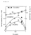
- FIG. 2 shows the way how the thermal resistivity (a reciprocal of the thermal conductivity) of the Si x Ge 1-x crystal changes according to the value of x at 20°C and 600°C, as typical examples of the lower and higher side temperatures, of respective two junctions, which comes to the maximum when x is around 0.6. This is supposed to be caused by phonon scattering.
- the addition of Ga raises the thermal resistivity slightly (the black circle and triangle in FIG. 2).
- the higher Ga concentration is, the more the thermal resistivity is expectantly.
- the specific heat increases with increase in the Si component.
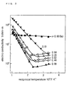
- Samples of 3 x 1 x 10 mm 3 were prepared from pulled crystals to measure the electric conductivity by means of the four-point probe method in which four probes are placed in a line on the sample and current is passed through the outer two probes and the potential developed across the inner two probes is measured.
- the change in the electric conductivity against the temperature is shown in FIG. 3.
- the electric conductivity exponentially increases with the temperature at 100 to 200°C and higher.
- the sample added with Ga shows an almost constant value of the electric conductivity up to a high temperature. It is expected that Ga addition with a higher concentration leads a higher and constant value of the electric conductivity up to a high temperature.
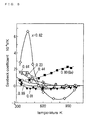
- the change in the intrinsic electric conductivity at 600°C according to the composition is shown in FIG. 4. It is seen that the richer Ge is, the higher the electric conductivity becomes. However, if impurities are added at a high concentration, a high value of the electric conductivity can be obtained even in an Si rich crystal. Further, the dependence of the bandgap against the composition is also shown.
- the pulled crystals were sliced into disk-shape samples 10 mm in diameter and 1 mm in thickness and using the samples the Seebeck coefficient was measured by means of a temperature difference method.
- the temperature difference method is to measure a thermoelectromotive force generated between both contact faces of a sample held between thermal blocks of different temperatures.
- FIG. 5 shows the change in the Seebeck coefficient against the temperature.
- the Seebeck coefficient remarkably changes from a positive value (a P-type semiconductor) to a negative value (a N-type semiconductor or an intrinsic semiconductor region) with samples of 0.6 to 0.8 in the composition, the values being high, respectively.
- the Seebeck coefficient increases monotonously with the temperature.
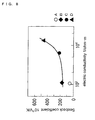
- FIG. 6 shows the dependence of the Seebeck coefficient against the composition at 600°C.
- the composition of around 0.8 a large absolute value thereof is expected.
- the composition of around 0.1 to 0.5 the difference in the mobility between electrons and holes is small in the composition of around 0.1 to 0.5 and hence a high value of the Seebeck coefficient cannot be expected.
- the thermal conductivity is low but the electric conductivity and the Seebeck coefficient are both high, but these values have been known first by the measurement of the inventors, and in view of working conditions (a temperature range) composition of Si x Ge 1-x (a value of x) and a dopant concentration may be determined in such a manner as the value of the performance index becomes as high as possible.
- the electric conductivity changes according to amounts of added dopants and increases almost in proportion to a concentration thereof.
- the Seebeck coefficient decreases with a dopant concentration and it has been known that the range of 10 18 to 10 20 (/cm 3 ) with around 10 19 /cm 3 as the center is theoretically preferred to attain a high performance index, so an SiGe crystal of a dopant concentration at this level is a preferred material from a practical viewpoint.
- Average grain diameters of the samples B and D were about 50 ⁇ m and about 200 ⁇ m, respectively and assuming that these grain shapes are spherical, the volumes thereof are about 6.5 x 10 -5 mm 3 and about 4.2 x 10 -3 mm 3 , respectively.
- Samples Crystalline state Si content (x) Dopant (Ga) concentration A single crystal 0.91 5.6 x 10 13 /cm 3 (non-doped) B polycrystal (about 50 ⁇ m in diameter) 0.80 2.0 x 10 17 /cm -3 C single crystal 0.95 1.3 x 10 19 /cm -3 D polycrystal (about 200 ⁇ m in diameter) 0.81 7.0 x 10 19 /cm -3
- the Si x Ge 1-x (0 ⁇ x ⁇ 1) crystal of the present invention there are realized great advantages that the performance index as the thermoelectric element can be improved, the crystal is excellent in machinability, and neither degradation in characteristics nor cracking occurs during use.
Landscapes
- Chemical & Material Sciences (AREA)
- Engineering & Computer Science (AREA)
- Crystallography & Structural Chemistry (AREA)
- Materials Engineering (AREA)
- Metallurgy (AREA)
- Organic Chemistry (AREA)
- Inorganic Chemistry (AREA)
- Crystals, And After-Treatments Of Crystals (AREA)
- Silicon Compounds (AREA)
- Compositions Of Oxide Ceramics (AREA)
Claims (20)
- Lingot de cristal de SixGe1-x (0 < x < 1), caractérisé en ce que les grains de cristal formant ledit lingot de cristal sont de 5 x 10⁻⁵ mm3 ou plus en volume.
- Lingot de cristal de SixGe1-x (0 < x < 1) selon la revendication 1, caractérisé en ce que ledit lingot de cristal est produit au moyen d'un procédé de tirage.
- Lingot de cristal de SixGe1-x (0 < x < 1) selon la revendication 1, caractérisé en ce que ledit lingot de cristal a une valeur absolue du coefficient de Seebeck dans la plage de 100 à 700 µV/K.
- Lingot de cristal de SixGe1-x (0 < x < 1) selon la revendication 2, caractérisé en ce que ledit lingot de cristal a une valeur absolue du coefficient de Seebeck dans la plage de 100 à 700 µV/K.
- Lingot de cristal de SixGe1-x (0 < x < 1) selon la revendication 1, caractérisé en ce que ledit lingot de cristal a une valeur de la conductivité thermique dans la plage de 1 à 20 W/m.K.
- Lingot de cristal de SixGe1-x (0 < x < 1) selon la revendication 2, caractérisé en ce que ledit lingot de cristal a une valeur de la conductivité thermique dans la plage de 1 à 20 W/m.K.
- Lingot de cristal de SixGe1-x (0 < x < 1) selon la revendication 1, caractérisé en ce que ledit lingot de cristal a une valeur de la conductivité électrique dans la plage de 101 à 105 W/Ω.m.
- Lingot de cristal de SixGe1-x (0 < x < 1) selon la revendication 2, caractérisé en ce que ledit lingot de cristal a une valeur de la conductivité électrique dans la plage de 101 à 105 W/Ω.m.
- Lingot de cristal de SixGe1-x (0 < x < 1) selon la revendication 1, caractérisé en ce que ledit lingot de cristal a une valeur absolue du coefficient de Seebeck dans la plage de 100 à 700 µV/K, une valeur de la conductivité thermique dans la plage de 1 à 20 W/m.K et une valeur de la conductivité électrique dans la plage de 101 à 105 W/Ω.m.
- Lingot de cristal de SixGe1-x (0 < x < 1) selon la revendication 2, caractérisé en ce que ledit lingot de cristal a une valeur absolue du coefficient de Seebeck dans la plage de 100 à 700 µV/K, une valeur de la conductivité thermique dans la plage de 1 à 20 W/m.K et une valeur de la conductivité électrique dans la plage de 101 à 105 W/Ω.m.
- Lingot de cristal de SixGe1-x (0 < x < 1) selon la revendication 1, caractérisé en ce que ledit lingot de cristal a une valeur de x dans la plage de 0,6 à 0,8.
- Lingot de cristal de SixGe1-x (0 < x < 1) selon la revendication 2, caractérisé en ce que ledit lingot de cristal a une valeur de x dans la plage de 0,6 à 0,8.
- Lingot de cristal de SixGe1-x (0 < x < 1) selon la revendication 1, caractérisé en ce qu'un élément sélectionné parmi B, Al ou Ga est ajouté au dit lingot de cristal.
- Lingot de cristal de SixGe1-x (0 < x < 1) selon la revendication 2, caractérisé en ce qu'un élément sélectionné parmi B, Al ou Ga est ajouté au dit lingot de cristal.
- Lingot de cristal de SixGe1-x (0 < x < 1) selon la revendication 1, caractérisé en ce qu'un élément sélectionné parmi P, As ou Sb est ajouté au dit lingot de cristal.
- Lingot de cristal de SixGe1-x (0 < x < 1) selon la revendication 2, caractérisé en ce qu'un élément sélectionné parmi P, As ou Sb est ajouté au dit lingot de cristal.
- Lingot de cristal de SixGe1-x (0 < x < 1) selon la revendication 1, caractérisé en ce que ledit lingot de cristal est un lingot monocristal.
- Lingot de cristal de SixGe1-x (0 < x < 1) selon la revendication 2, caractérisé en ce que ledit lingot de cristal est un lingot monocristal.
- Elément thermoélectrique, caractérisé par l'utilisation dudit lingot de cristal de SixGe1-x (0 < x < 1) selon la revendication 1.
- Elément thermoélectrique, caractérisé par l'utilisation dudit lingot de cristal de SixGe1-x (0 < x < 1) selon la revendication 2.
Applications Claiming Priority (3)
| Application Number | Priority Date | Filing Date | Title |
|---|---|---|---|
| JP33589498 | 1998-11-26 | ||
| JP33589498 | 1998-11-26 | ||
| PCT/JP1999/006168 WO2000030975A1 (fr) | 1998-11-26 | 1999-11-05 | CRISTAL SiGe |
Publications (3)
| Publication Number | Publication Date |
|---|---|
| EP1052222A1 EP1052222A1 (fr) | 2000-11-15 |
| EP1052222A4 EP1052222A4 (fr) | 2002-02-13 |
| EP1052222B1 true EP1052222B1 (fr) | 2004-09-29 |
Family
ID=18293571
Family Applications (1)
| Application Number | Title | Priority Date | Filing Date |
|---|---|---|---|
| EP99954399A Expired - Lifetime EP1052222B1 (fr) | 1998-11-26 | 1999-11-05 | CRISTAL SiGe |
Country Status (8)
| Country | Link |
|---|---|
| US (1) | US6498288B1 (fr) |
| EP (1) | EP1052222B1 (fr) |
| JP (1) | JP3975676B2 (fr) |
| KR (1) | KR100654486B1 (fr) |
| CN (1) | CN1130308C (fr) |
| DE (1) | DE69920662T2 (fr) |
| RU (1) | RU2206643C2 (fr) |
| WO (1) | WO2000030975A1 (fr) |
Families Citing this family (5)
| Publication number | Priority date | Publication date | Assignee | Title |
|---|---|---|---|---|
| JP2002094131A (ja) * | 2000-09-13 | 2002-03-29 | Sumitomo Special Metals Co Ltd | 熱電変換素子 |
| CN100459202C (zh) * | 2007-07-02 | 2009-02-04 | 北京科技大学 | 一种硅锗系热电材料的制备方法 |
| JP7476191B2 (ja) * | 2019-07-03 | 2024-04-30 | 住友電気工業株式会社 | 熱電変換材料、熱電変換素子、熱電変換モジュールおよび光センサ |
| RU2739887C1 (ru) * | 2020-05-06 | 2020-12-29 | Федеральное государственное автономное образовательное учреждение высшего образования "Национальный исследовательский Нижегородский государственный университет им. Н.И. Лобачевского" | СПОСОБ ПОЛУЧЕНИЯ ТЕРМОЭЛЕКТРИЧЕСКОГО МАТЕРИАЛА n-ТИПА ПРОВОДИМОСТИ НА ОСНОВЕ ТВЕРДОГО РАСТВОРА Gex-δSi1-xSbδ ПРИ х=0,26-0,36, δ=0,008-0,01 |
| CN113921690B (zh) * | 2021-08-30 | 2026-01-09 | 桂林电子科技大学 | 一种硼、铝双掺的硅锗基热电材料及其制备方法 |
Family Cites Families (6)
| Publication number | Priority date | Publication date | Assignee | Title |
|---|---|---|---|---|
| BE537841A (fr) * | 1954-05-03 | 1900-01-01 | ||
| GB8431071D0 (en) * | 1984-12-08 | 1985-01-16 | Univ Glasgow | Alloys |
| JP2686928B2 (ja) * | 1985-08-26 | 1997-12-08 | アンリツ株式会社 | シリコン・ゲルマニウム混晶薄膜導電体 |
| JPH04285096A (ja) * | 1991-03-12 | 1992-10-09 | Nec Corp | Si−Ge単結晶育成法 |
| JP3313412B2 (ja) * | 1992-07-07 | 2002-08-12 | 徳三 助川 | 半導体結晶の製造方法および装置 |
| JPH07321323A (ja) * | 1994-05-24 | 1995-12-08 | Matsushita Electric Ind Co Ltd | 薄膜トランジスタおよびその製造方法 |
-
1999
- 1999-11-05 RU RU2000122450/12A patent/RU2206643C2/ru not_active IP Right Cessation
- 1999-11-05 DE DE69920662T patent/DE69920662T2/de not_active Expired - Fee Related
- 1999-11-05 CN CN99802262A patent/CN1130308C/zh not_active Expired - Fee Related
- 1999-11-05 KR KR1020007007308A patent/KR100654486B1/ko not_active Expired - Fee Related
- 1999-11-05 EP EP99954399A patent/EP1052222B1/fr not_active Expired - Lifetime
- 1999-11-05 US US09/582,237 patent/US6498288B1/en not_active Expired - Fee Related
- 1999-11-05 JP JP2000583811A patent/JP3975676B2/ja not_active Expired - Lifetime
- 1999-11-05 WO PCT/JP1999/006168 patent/WO2000030975A1/fr not_active Ceased
Also Published As
| Publication number | Publication date |
|---|---|
| EP1052222A1 (fr) | 2000-11-15 |
| JP3975676B2 (ja) | 2007-09-12 |
| RU2206643C2 (ru) | 2003-06-20 |
| CN1130308C (zh) | 2003-12-10 |
| KR100654486B1 (ko) | 2006-12-05 |
| DE69920662T2 (de) | 2005-02-10 |
| CN1288443A (zh) | 2001-03-21 |
| US6498288B1 (en) | 2002-12-24 |
| DE69920662D1 (de) | 2004-11-04 |
| EP1052222A4 (fr) | 2002-02-13 |
| KR20010033781A (ko) | 2001-04-25 |
| WO2000030975A1 (fr) | 2000-06-02 |
Similar Documents
| Publication | Publication Date | Title |
|---|---|---|
| Yim et al. | Thermoelectric properties of Bi2Te3-Sb2Te3-Sb2Se3 pseudo-ternary alloys in the temperature range 77 to 300 K | |
| Jeon et al. | Electrical and thermoelectrical properties of undoped Bi2Te3-Sb2Te3 and Bi2Te3-Sb2Te3-Sb2Se3 single crystals | |
| Yamashita et al. | High-performance bismuth-telluride compounds with highly stable thermoelectric figure of merit | |
| Yonenaga et al. | Thermal and electrical properties of Czochralski grown GeSi single crystals | |
| Yamashita et al. | Effect of annealing on thermoelectric properties of bismuth telluride compounds | |
| US6319744B1 (en) | Method for manufacturing a thermoelectric semiconductor material or element and method for manufacturing a thermoelectric module | |
| EP3246959B1 (fr) | Matériau thermoélectrique à semi-conducteurs composés et procédé de fabrication correspondant | |
| Perrin et al. | Study of the n-type Bi2Te2. 7Se0. 3 doped with bromine impurity | |
| US20030168094A1 (en) | Thermoelectric material and process for manufacturing the same | |
| EP1052222B1 (fr) | CRISTAL SiGe | |
| Su | Thermal stability of melt grown Tl-doped PbTeSe material for thermoelectric applications | |
| Kavei et al. | Fabrication and characterization of the p-type (Bi 2 Te 3) x (Sb 2 Te 3) 1-x thermoelectric crystals prepared via zone melting. | |
| Ettenberg et al. | A new n-type and improved p-type pseudo-ternary (Bi 2 Te 3)(Sb 2 Te 3)(Sb 2 Se 3) alloy for Peltier cooling | |
| Vandersande et al. | Effect of high temperature annealing on the thermoelectric properties of GaP doped SiGe | |
| Crocker et al. | Some physical properties of the PbTe-MgTe alloy system | |
| JPH0832588B2 (ja) | 熱電半導体材料およびその製造方法 | |
| JPWO2000030975A1 (ja) | SiGe結晶 | |
| Harman et al. | PbTe-based quantum-dot thermoelectric materials with high ZT | |
| JP3952354B2 (ja) | SiGe結晶およびその製造方法 | |
| Yamashita et al. | Influence of annealing on the distribution of thermoelectric figure of merit in bismuth-telluride ingots | |
| Satou et al. | Influence of annealing on the spatial distribution of thermoelectric properties in bismuth-telluride specimens | |
| Bhatta et al. | Properties of p-and n-Type PbTe microwires for thermoelectric devices | |
| KR102938414B1 (ko) | BiTe계 n형-열전재료 제조용 분말, 이를 이용하여 제조된 BiTe계 n형- 열전재료 및 이의 제조방법 | |
| Pickering et al. | Variation of carrier concentration in Pb0. 8Sn0. 2Te with annealing and growth temperature | |
| Yonenaga et al. | Thermal and electrical properties of Czochralski grown GeSi alloys |
Legal Events
| Date | Code | Title | Description |
|---|---|---|---|
| PUAI | Public reference made under article 153(3) epc to a published international application that has entered the european phase |
Free format text: ORIGINAL CODE: 0009012 |
|
| 17P | Request for examination filed |
Effective date: 20000811 |
|
| AK | Designated contracting states |
Kind code of ref document: A1 Designated state(s): AT BE CH CY DE DK ES FI FR GB GR IE IT LI LU MC NL PT SE |
|
| A4 | Supplementary search report drawn up and despatched |
Effective date: 20020103 |
|
| AK | Designated contracting states |
Kind code of ref document: A4 Designated state(s): AT BE CH CY DE DK ES FI FR GB GR IE IT LI LU MC NL PT SE |
|
| 17Q | First examination report despatched |
Effective date: 20030331 |
|
| GRAP | Despatch of communication of intention to grant a patent |
Free format text: ORIGINAL CODE: EPIDOSNIGR1 |
|
| RBV | Designated contracting states (corrected) |
Designated state(s): DE FR GB IT |
|
| GRAS | Grant fee paid |
Free format text: ORIGINAL CODE: EPIDOSNIGR3 |
|
| GRAA | (expected) grant |
Free format text: ORIGINAL CODE: 0009210 |
|
| AK | Designated contracting states |
Kind code of ref document: B1 Designated state(s): DE FR GB IT |
|
| PG25 | Lapsed in a contracting state [announced via postgrant information from national office to epo] |
Ref country code: IT Free format text: LAPSE BECAUSE OF FAILURE TO SUBMIT A TRANSLATION OF THE DESCRIPTION OR TO PAY THE FEE WITHIN THE PRESCRIBED TIME-LIMIT;WARNING: LAPSES OF ITALIAN PATENTS WITH EFFECTIVE DATE BEFORE 2007 MAY HAVE OCCURRED AT ANY TIME BEFORE 2007. THE CORRECT EFFECTIVE DATE MAY BE DIFFERENT FROM THE ONE RECORDED. Effective date: 20040929 Ref country code: FR Free format text: LAPSE BECAUSE OF FAILURE TO SUBMIT A TRANSLATION OF THE DESCRIPTION OR TO PAY THE FEE WITHIN THE PRESCRIBED TIME-LIMIT Effective date: 20040929 |
|
| REG | Reference to a national code |
Ref country code: GB Ref legal event code: FG4D |
|
| REG | Reference to a national code |
Ref country code: IE Ref legal event code: FG4D |
|
| REF | Corresponds to: |
Ref document number: 69920662 Country of ref document: DE Date of ref document: 20041104 Kind code of ref document: P |
|
| PG25 | Lapsed in a contracting state [announced via postgrant information from national office to epo] |
Ref country code: GB Free format text: LAPSE BECAUSE OF NON-PAYMENT OF DUE FEES Effective date: 20041229 |
|
| PLBE | No opposition filed within time limit |
Free format text: ORIGINAL CODE: 0009261 |
|
| STAA | Information on the status of an ep patent application or granted ep patent |
Free format text: STATUS: NO OPPOSITION FILED WITHIN TIME LIMIT |
|
| GBPC | Gb: european patent ceased through non-payment of renewal fee |
Effective date: 20041229 |
|
| 26N | No opposition filed |
Effective date: 20050630 |
|
| EN | Fr: translation not filed | ||
| PGFP | Annual fee paid to national office [announced via postgrant information from national office to epo] |
Ref country code: DE Payment date: 20081103 Year of fee payment: 10 |
|
| PG25 | Lapsed in a contracting state [announced via postgrant information from national office to epo] |
Ref country code: DE Free format text: LAPSE BECAUSE OF NON-PAYMENT OF DUE FEES Effective date: 20100601 |