EP1052690A2 - Procédé de fabrication de dispositifs à grille MOS avec des tranchées auto-alignées - Google Patents
Procédé de fabrication de dispositifs à grille MOS avec des tranchées auto-alignées Download PDFInfo
- Publication number
- EP1052690A2 EP1052690A2 EP00108965A EP00108965A EP1052690A2 EP 1052690 A2 EP1052690 A2 EP 1052690A2 EP 00108965 A EP00108965 A EP 00108965A EP 00108965 A EP00108965 A EP 00108965A EP 1052690 A2 EP1052690 A2 EP 1052690A2
- Authority
- EP
- European Patent Office
- Prior art keywords
- layer
- well
- mask
- source
- semiconductor
- Prior art date
- Legal status (The legal status is an assumption and is not a legal conclusion. Google has not performed a legal analysis and makes no representation as to the accuracy of the status listed.)
- Withdrawn
Links
Images


Classifications
-
- H—ELECTRICITY
- H10—SEMICONDUCTOR DEVICES; ELECTRIC SOLID-STATE DEVICES NOT OTHERWISE PROVIDED FOR
- H10D—INORGANIC ELECTRIC SEMICONDUCTOR DEVICES
- H10D30/00—Field-effect transistors [FET]
- H10D30/60—Insulated-gate field-effect transistors [IGFET]
- H10D30/64—Double-diffused metal-oxide semiconductor [DMOS] FETs
- H10D30/66—Vertical DMOS [VDMOS] FETs
-
- H—ELECTRICITY
- H10—SEMICONDUCTOR DEVICES; ELECTRIC SOLID-STATE DEVICES NOT OTHERWISE PROVIDED FOR
- H10D—INORGANIC ELECTRIC SEMICONDUCTOR DEVICES
- H10D30/00—Field-effect transistors [FET]
- H10D30/01—Manufacture or treatment
- H10D30/021—Manufacture or treatment of FETs having insulated gates [IGFET]
- H10D30/028—Manufacture or treatment of FETs having insulated gates [IGFET] of double-diffused metal oxide semiconductor [DMOS] FETs
- H10D30/0291—Manufacture or treatment of FETs having insulated gates [IGFET] of double-diffused metal oxide semiconductor [DMOS] FETs of vertical DMOS [VDMOS] FETs
- H10D30/0297—Manufacture or treatment of FETs having insulated gates [IGFET] of double-diffused metal oxide semiconductor [DMOS] FETs of vertical DMOS [VDMOS] FETs using recessing of the gate electrodes, e.g. to form trench gate electrodes
-
- H—ELECTRICITY
- H10—SEMICONDUCTOR DEVICES; ELECTRIC SOLID-STATE DEVICES NOT OTHERWISE PROVIDED FOR
- H10D—INORGANIC ELECTRIC SEMICONDUCTOR DEVICES
- H10D30/00—Field-effect transistors [FET]
- H10D30/60—Insulated-gate field-effect transistors [IGFET]
- H10D30/64—Double-diffused metal-oxide semiconductor [DMOS] FETs
- H10D30/66—Vertical DMOS [VDMOS] FETs
- H10D30/668—Vertical DMOS [VDMOS] FETs having trench gate electrodes, e.g. UMOS transistors
-
- H—ELECTRICITY
- H10—SEMICONDUCTOR DEVICES; ELECTRIC SOLID-STATE DEVICES NOT OTHERWISE PROVIDED FOR
- H10D—INORGANIC ELECTRIC SEMICONDUCTOR DEVICES
- H10D30/00—Field-effect transistors [FET]
- H10D30/01—Manufacture or treatment
- H10D30/021—Manufacture or treatment of FETs having insulated gates [IGFET]
- H10D30/028—Manufacture or treatment of FETs having insulated gates [IGFET] of double-diffused metal oxide semiconductor [DMOS] FETs
- H10D30/0291—Manufacture or treatment of FETs having insulated gates [IGFET] of double-diffused metal oxide semiconductor [DMOS] FETs of vertical DMOS [VDMOS] FETs
- H10D30/0295—Manufacture or treatment of FETs having insulated gates [IGFET] of double-diffused metal oxide semiconductor [DMOS] FETs of vertical DMOS [VDMOS] FETs using recessing of the source electrodes
-
- H—ELECTRICITY
- H10—SEMICONDUCTOR DEVICES; ELECTRIC SOLID-STATE DEVICES NOT OTHERWISE PROVIDED FOR
- H10D—INORGANIC ELECTRIC SEMICONDUCTOR DEVICES
- H10D64/00—Electrodes of devices having potential barriers
- H10D64/20—Electrodes characterised by their shapes, relative sizes or dispositions
- H10D64/23—Electrodes carrying the current to be rectified, amplified, oscillated or switched, e.g. sources, drains, anodes or cathodes
- H10D64/251—Source or drain electrodes for field-effect devices
- H10D64/252—Source or drain electrodes for field-effect devices for vertical or pseudo-vertical devices
- H10D64/2527—Source or drain electrodes for field-effect devices for vertical or pseudo-vertical devices for vertical devices wherein the source or drain electrodes are recessed in semiconductor bodies
-
- H—ELECTRICITY
- H10—SEMICONDUCTOR DEVICES; ELECTRIC SOLID-STATE DEVICES NOT OTHERWISE PROVIDED FOR
- H10D—INORGANIC ELECTRIC SEMICONDUCTOR DEVICES
- H10D64/00—Electrodes of devices having potential barriers
- H10D64/20—Electrodes characterised by their shapes, relative sizes or dispositions
- H10D64/23—Electrodes carrying the current to be rectified, amplified, oscillated or switched, e.g. sources, drains, anodes or cathodes
- H10D64/251—Source or drain electrodes for field-effect devices
- H10D64/256—Source or drain electrodes for field-effect devices for lateral devices wherein the source or drain electrodes are recessed in semiconductor bodies
Definitions
- the present invention relates to semiconductor devices and, more particularly, to process for forming MOS-gated devices having sell-aligned trenches.
- An MOS transistor that includes a trench gate structure offers important advantages over a planar transistor for high current, low voltage switching applications. In the latter configuration, constriction occurs at high current flows, an effect that places substantial constraints on the design of a transistor intended for operation under such conditions.
- a trench gate of a DMOS device typically includes a trench extending from the source to the drain and having sidewalls and a floor that are each lined with a layer of thermally grown silicon dioxide.
- the lined trench is filled with doped polysilicon.
- the structure of the trench gate allows less constricted current flow and, consequently, provides lower values of specific on-resistance.
- the trench gate makes possible a decreased cell pitch in an MOS channel extending along the vertical sidewalls of the trench from the bottom of the source across the body of the transistor to the drain below. Channel density is thereby increased, which reduces the contribution of the channel to on-resistance.
- trench DMOS transistors The structure and performance of trench DMOS transistors are disclosed in Bulucea and Rossen, "Trench DMOS Transistor Technology for High-Current (100 A Range) Switching," in Solid-State Electronics, 1991, Vol. 34, No. 5, pp 493-507.
- trench gates are also advantageously employed in insulated gate bipolar transistors (IGBTs), MOS-controlled thyristors (MCTs), and other MOS-gated devices.
- U.S. Patent No. 5,393,704 discloses a method of forming in and on a substrate a self-aligned trench contact for a device region that includes gate electrodes on the semiconductor substrate, source/drain regions within the substrate, and spacers on the gate electrode sidewalls.
- the sidewall spacers are used as a mask to provide an opening to the substrate where the trench contact is to be formed.
- U.S. Patent No. 5,716,886 discloses a method of fabricating a high-voltage MOS device in which a silicon nitride layer is used as a mask to form trench type source/drain regions in a substrate.
- the trench source/drain regions contain two conductive layers; portions of the same two conductive layers are included in a gate on the substrate surface.
- U.S. Patent No. 5,665,619 discloses a method of fabricating a DMOS transistor having self-aligned contact trenches that are etched through a masked oxide/nitride/oxide (ONO) sandwich on a silicon substrate.
- Gate polysilicon is deposited in the trenches and planarized with the nitride layer.
- the planarized polysilicon is covered with oxide; doping and four additional photolithographic masking steps are employed to form N+ source regions adjacent to the trenches and a P+ body ohmic content region between the source regions.
- the present invention includes a process for forming an MOS-gated device having self-aligned trenches, said process comprising:
- the invention also includes a process for forming a sell-aligned gate trench in a vertical MOS device, said process comprising:
- the present invention is directed to a process for forming an MOS-gated device having self-aligned trenches.
- a screen oxide layer is formed on an upper layer of a semiconductor substrate, and a nitride layer is formed on the screen oxide layer.
- the nitride layer is patterned and etched to define a well region in the upper layer, and ions of a first conduction type are diffused into the masked upper layer to form the well region.
- Ions of a second, opposite conduction type are implanted into the well region of the masked upper layer to form a source region extending to a selected depth that defines a source-well junction.
- the well mask is removed, exposing the portion of the nitride layer previously underlying the mask.
- An oxide insulating layer providing a hard mask is formed overlying the well and source regions in the upper layer. The remaining portions of the nitride layer and the screen oxide layer underlying it, which had been protected by the well mask, are removed, thereby exposing the portion of the substrate not masked by the oxide insulating layer.
- the portion of the substrate thus exposed is etched to form a gate trench extending through the substrate to a selected depth beneath the well region.
- Sidewalls and a floor of an insulator are formed in the gate trench, which is filled with a semiconductor.
- the semiconductor in the trench is planarized to be substantially coplanar with the upper surface of the oxide insulating layer.
- An interlevel dielectric layer is formed on the planarized gate trench semiconductor and the upper surface of the oxide insulating layer. Following formation of a contact window mask on the interlevel dielectric layer, it and the underlying oxide insulating layer are etched to form contact openings to gate semiconductor and the source region.
- the gate semiconductor and the source region are simultaneously etched through the contact openings, the source region being etched to a depth substantially corresponding to the depth of the source-well junction. Ions of the first conduction type are implanted through the contact openings into the gate semiconductor and the source region.
- the contact window mask is removed, and metal is deposited on the interlevel dielectric layer and in the contact openings, then patterned to form discrete source and gate connectors.
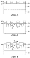
- a semiconductor substrate 101 has an upper layer 102, on which is formed a thin screen oxide layer 103.
- a nitride layer 104 is deposited on layer 103 and patterned by a photoresist well mask WM.
- Semiconductor substrate 101 preferably comprises monocrystalline silicon, upper layer 102 comprises epitaxially grown silicon, and screen layer 103 comprises silicon dioxide.
- the deposition of nitride layer 104 can be carried out by chemical vapor deposition (CVD) or low pressure chemical vapor deposition (LPCVD).
- well regions 105 are formed by implantation and diffusion by ions of a first conduction type, following which source regions 106 are formed by implantation and diffusion of ions of a second, opposite conduction type to a selected depth that defines a source-well junction 107.
- well mask WM is stripped from screen layer 103.
- the first conduction type is represented as P, producing P-well regions 105, and the second conduction type is N, resulting in N+ source regions 106. It is understood that these conduction types can each be reversed to the opposite type. Boron is a preferred P dopant; arsenic and phosphorus are useful N dopants.
- an oxide insulating layer 108 silicon dioxide is formed over source regions 106 and well regions 105.
- Nitride layer 104 is then removed by selective etching, leaving the structure depicted in FIG. 1-4.
- Oxide insulating layer 108 which has substantially vertical sidewalls 110, provides a hard mask for the etching of trenches 111, which extend substantially to a selected depth 112 below that of well regions 105, as shown in FIG. 1-5.
- Insulating sidewalls 112 and floor 113 preferably comprising silicon dioxide, are formed in trenches 111, as depicted in FIG. 1-6.
- Trenches 111 are filled with a semiconductor 114, comprising polysilicon.
- the semiconductor 114 is planarized by etching or mechanical processing to provide a surface 115 that is substantially coplanar with surface 109 of oxide insulating layer 108.
- an interlevel dielectric layer 116 is deposited on surfaces 109 and 115 and patterned and etched using a contact window mask (not shown) to provide trench contact openings 117 and source contact openings 118.
- the interlevel dielectric layer 116 can be formed from, for example borophosphosilicate glass (BPSG). Silicon dimple etching using the patterned interlevel dielectric layer 116 as a hard mask is employed to extend trench contact openings 117 to depth 119 and source contact openings 118 through source regions 106 substantially to source-well junctions 107. Implantation and diffusion of ions of the first conduction type through contact openings 117 and 118 produces P+ regions 120 in gate semiconductor 114 and P+ emitter regions 121 adjacent to source regions 106.
- BPSG borophosphosilicate glass
- a metal such as aluminum is deposited and patterned, as shown in FIG. 1-9, to provide gate connectors 122 and source/ emitter connectors 123, thereby completing the fabrication of device 100 in accordance with the present invention.
- oxide insulating layer 108 and interlevel dielectric layer 116 as hard masks and requires only three photolithographic masks (well, contact window, and metal), is significantly simpler and more convenient than typical known device fabrication processes.
- a screen oxide layer is formed on an upper layer of a semiconductor substrate, and a nitride layer is formed on the screen oxide layer.
- the nitride layer is patterned and etched to define a well region in the upper layer, and ions of a first conduction type are diffused into the masked upper layer to form the well region.
- Ions of a second, opposite conduction type are implanted into the well region of the masked upper layer to form a source region extending to a selected depth that defines a source-well junction.
- the well mask is removed, exposing the portion of the nitride layer previously underlying the mask.
- An oxide insulating layer providing a hard mask is formed overlying the well and source regions in the upper layer. The remaining portions of the nitride layer and the screen oxide layer underlying it, which had been protected by the well mask, are removed, thereby exposing the portion of the substrate not masked by the oxide insulating layer.
- the portion of the substrate thus exposed is etched to form a gate trench extending through the substrate to a selected depth beneath the well region.
- Sidewalls and a floor of an insulator are formed in the gate trench, which is filled with a semiconductor.
- the semiconductor in the trench is planarized to be substantially coplanar with the upper surface of the oxide insulating layer.
- An interlevel dielectric layer is formed on the planarized gate trench semiconductor and the upper surface of the oxide insulating layer.
Landscapes
- Thyristors (AREA)
- Insulated Gate Type Field-Effect Transistor (AREA)
- Metal-Oxide And Bipolar Metal-Oxide Semiconductor Integrated Circuits (AREA)
Applications Claiming Priority (2)
| Application Number | Priority Date | Filing Date | Title |
|---|---|---|---|
| US09/307,879 US6238981B1 (en) | 1999-05-10 | 1999-05-10 | Process for forming MOS-gated devices having self-aligned trenches |
| US307879 | 1999-05-10 |
Publications (2)
| Publication Number | Publication Date |
|---|---|
| EP1052690A2 true EP1052690A2 (fr) | 2000-11-15 |
| EP1052690A3 EP1052690A3 (fr) | 2003-12-03 |
Family
ID=23191551
Family Applications (1)
| Application Number | Title | Priority Date | Filing Date |
|---|---|---|---|
| EP00108965A Withdrawn EP1052690A3 (fr) | 1999-05-10 | 2000-04-27 | Procédé de fabrication de dispositifs à grille MOS avec des tranchées auto-alignées |
Country Status (4)
| Country | Link |
|---|---|
| US (1) | US6238981B1 (fr) |
| EP (1) | EP1052690A3 (fr) |
| JP (1) | JP4711486B2 (fr) |
| KR (1) | KR100727452B1 (fr) |
Cited By (5)
| Publication number | Priority date | Publication date | Assignee | Title |
|---|---|---|---|---|
| US6251746B1 (en) * | 1998-10-09 | 2001-06-26 | Samsung Electronics Co., Ltd. | Methods of forming trench isolation regions having stress-reducing nitride layers therein |
| US6465866B2 (en) | 1999-10-12 | 2002-10-15 | Samsung Electronics Co., Ltd. | Trench isolation regions having trench liners with recessed ends |
| CN103187291A (zh) * | 2011-12-29 | 2013-07-03 | 立新半导体有限公司 | 一种制备沟槽半导体功率分立器件的方法 |
| CN103824774A (zh) * | 2012-11-16 | 2014-05-28 | 竹懋科技股份有限公司 | 沟渠式mos整流器及其制造方法 |
| CN115084247A (zh) * | 2022-08-22 | 2022-09-20 | 泰科天润半导体科技(北京)有限公司 | 一种双沟槽型碳化硅mosfet的制造方法 |
Families Citing this family (27)
| Publication number | Priority date | Publication date | Assignee | Title |
|---|---|---|---|---|
| JP2000196075A (ja) * | 1998-12-25 | 2000-07-14 | Hitachi Ltd | 半導体装置及びその製造方法 |
| US7098506B2 (en) | 2000-06-28 | 2006-08-29 | Renesas Technology Corp. | Semiconductor device and method for fabricating the same |
| EP1089343A3 (fr) | 1999-09-30 | 2003-12-17 | Kabushiki Kaisha Toshiba | Dispositif semi-conducteur à grille enterrée |
| JP3356162B2 (ja) * | 1999-10-19 | 2002-12-09 | 株式会社デンソー | 半導体装置及びその製造方法 |
| KR100400079B1 (ko) * | 2001-10-10 | 2003-09-29 | 한국전자통신연구원 | 트랜치 게이트 구조를 갖는 전력용 반도체 소자의 제조 방법 |
| JP3715971B2 (ja) * | 2003-04-02 | 2005-11-16 | ローム株式会社 | 半導体装置 |
| TWI223448B (en) * | 2003-04-29 | 2004-11-01 | Mosel Vitelic Inc | DMOS device having a trenched bus structure |
| US20070157516A1 (en) * | 2006-01-09 | 2007-07-12 | Fischer Bernhard A | Staged modular hydrocarbon reformer with internal temperature management |
| US9437729B2 (en) * | 2007-01-08 | 2016-09-06 | Vishay-Siliconix | High-density power MOSFET with planarized metalization |
| US9947770B2 (en) * | 2007-04-03 | 2018-04-17 | Vishay-Siliconix | Self-aligned trench MOSFET and method of manufacture |
| US9484451B2 (en) * | 2007-10-05 | 2016-11-01 | Vishay-Siliconix | MOSFET active area and edge termination area charge balance |
| US9443974B2 (en) | 2009-08-27 | 2016-09-13 | Vishay-Siliconix | Super junction trench power MOSFET device fabrication |
| US9431530B2 (en) * | 2009-10-20 | 2016-08-30 | Vishay-Siliconix | Super-high density trench MOSFET |
| KR101131892B1 (ko) * | 2010-03-31 | 2012-04-03 | 주식회사 하이닉스반도체 | 매립 게이트를 갖는 반도체 장치 및 그의 제조 방법 |
| CN103187287B (zh) * | 2011-12-29 | 2016-08-10 | 立新半导体有限公司 | 一种沟槽半导体分立器件的制备方法 |
| US9614043B2 (en) | 2012-02-09 | 2017-04-04 | Vishay-Siliconix | MOSFET termination trench |
| US9842911B2 (en) | 2012-05-30 | 2017-12-12 | Vishay-Siliconix | Adaptive charge balanced edge termination |
| US9887259B2 (en) | 2014-06-23 | 2018-02-06 | Vishay-Siliconix | Modulated super junction power MOSFET devices |
| CN115483211A (zh) | 2014-08-19 | 2022-12-16 | 维西埃-硅化物公司 | 电子电路 |
| CN106575666B (zh) | 2014-08-19 | 2021-08-06 | 维西埃-硅化物公司 | 超结金属氧化物半导体场效应晶体管 |
| US9396958B2 (en) * | 2014-10-14 | 2016-07-19 | Tokyo Electron Limited | Self-aligned patterning using directed self-assembly of block copolymers |
| CN110770299B (zh) | 2017-06-28 | 2022-06-07 | 旭化成株式会社 | 树脂组合物、树脂组合物的制造方法和成型体 |
| JP2019046991A (ja) * | 2017-09-04 | 2019-03-22 | ルネサスエレクトロニクス株式会社 | 半導体装置およびその製造方法 |
| US10770302B2 (en) * | 2018-09-27 | 2020-09-08 | Taiwan Semiconductor Manufacturing Company, Ltd. | Semiconductor FinFET device and method |
| DE102019104629B4 (de) | 2018-09-27 | 2022-10-20 | Taiwan Semiconductor Manufacturing Co., Ltd. | FinFET-Halbleiter-Bauelement und Verfahren |
| CN116759451A (zh) * | 2021-11-25 | 2023-09-15 | 成都森未科技有限公司 | 一种自对准沟槽栅结构igbt |
| CN117637607A (zh) * | 2024-01-24 | 2024-03-01 | 北京智芯微电子科技有限公司 | 超结半导体的自对准接触槽形成方法及超结半导体结构 |
Family Cites Families (20)
| Publication number | Priority date | Publication date | Assignee | Title |
|---|---|---|---|---|
| US583023A (en) * | 1897-05-25 | Hungary | ||
| JPS6040717B2 (ja) * | 1977-06-10 | 1985-09-12 | ソニー株式会社 | 半導体装置 |
| JPS5718365A (en) * | 1980-07-08 | 1982-01-30 | Matsushita Electronics Corp | Semiconductor device and manufacture thereof |
| US4983535A (en) * | 1981-10-15 | 1991-01-08 | Siliconix Incorporated | Vertical DMOS transistor fabrication process |
| US4767722A (en) * | 1986-03-24 | 1988-08-30 | Siliconix Incorporated | Method for making planar vertical channel DMOS structures |
| US5082795A (en) * | 1986-12-05 | 1992-01-21 | General Electric Company | Method of fabricating a field effect semiconductor device having a self-aligned structure |
| US5100823A (en) * | 1988-02-29 | 1992-03-31 | Motorola, Inc. | Method of making buried stacked transistor-capacitor |
| US5726463A (en) * | 1992-08-07 | 1998-03-10 | General Electric Company | Silicon carbide MOSFET having self-aligned gate structure |
| US5316959A (en) * | 1992-08-12 | 1994-05-31 | Siliconix, Incorporated | Trenched DMOS transistor fabrication using six masks |
| JP2912508B2 (ja) * | 1992-11-13 | 1999-06-28 | シャープ株式会社 | 縦型mosトランジスタの製造方法 |
| US5393704A (en) | 1993-12-13 | 1995-02-28 | United Microelectronics Corporation | Self-aligned trenched contact (satc) process |
| US5567634A (en) * | 1995-05-01 | 1996-10-22 | National Semiconductor Corporation | Method of fabricating self-aligned contact trench DMOS transistors |
| KR0143459B1 (ko) * | 1995-05-22 | 1998-07-01 | 한민구 | 모오스 게이트형 전력 트랜지스터 |
| US5684319A (en) * | 1995-08-24 | 1997-11-04 | National Semiconductor Corporation | Self-aligned source and body contact structure for high performance DMOS transistors and method of fabricating same |
| US5721148A (en) * | 1995-12-07 | 1998-02-24 | Fuji Electric Co. | Method for manufacturing MOS type semiconductor device |
| JP4077529B2 (ja) * | 1996-05-22 | 2008-04-16 | フェアチャイルドコリア半導体株式会社 | トレンチ拡散mosトランジスタの製造方法 |
| JPH09331062A (ja) * | 1996-06-11 | 1997-12-22 | Mitsubishi Electric Corp | 半導体装置およびその製造方法 |
| TW328619B (en) | 1996-09-21 | 1998-03-21 | United Microelectronics Corp | The high-pressure MOS and its manufacturing method |
| US5940689A (en) * | 1997-06-30 | 1999-08-17 | Harris Corporation | Method of fabricating UMOS semiconductor devices using a self-aligned, reduced mask process |
| JP3326366B2 (ja) * | 1997-08-08 | 2002-09-24 | 三洋電機株式会社 | 半導体装置及びその製造方法 |
-
1999
- 1999-05-10 US US09/307,879 patent/US6238981B1/en not_active Expired - Fee Related
-
2000
- 2000-04-27 EP EP00108965A patent/EP1052690A3/fr not_active Withdrawn
- 2000-05-04 KR KR1020000023854A patent/KR100727452B1/ko not_active Expired - Fee Related
- 2000-05-09 JP JP2000136015A patent/JP4711486B2/ja not_active Expired - Fee Related
Cited By (7)
| Publication number | Priority date | Publication date | Assignee | Title |
|---|---|---|---|---|
| US6251746B1 (en) * | 1998-10-09 | 2001-06-26 | Samsung Electronics Co., Ltd. | Methods of forming trench isolation regions having stress-reducing nitride layers therein |
| US6465866B2 (en) | 1999-10-12 | 2002-10-15 | Samsung Electronics Co., Ltd. | Trench isolation regions having trench liners with recessed ends |
| CN103187291A (zh) * | 2011-12-29 | 2013-07-03 | 立新半导体有限公司 | 一种制备沟槽半导体功率分立器件的方法 |
| CN103187291B (zh) * | 2011-12-29 | 2016-02-10 | 立新半导体有限公司 | 一种制备沟槽半导体功率分立器件的方法 |
| CN103824774A (zh) * | 2012-11-16 | 2014-05-28 | 竹懋科技股份有限公司 | 沟渠式mos整流器及其制造方法 |
| CN103824774B (zh) * | 2012-11-16 | 2017-04-12 | 竹懋科技股份有限公司 | 沟渠式mos整流器及其制造方法 |
| CN115084247A (zh) * | 2022-08-22 | 2022-09-20 | 泰科天润半导体科技(北京)有限公司 | 一种双沟槽型碳化硅mosfet的制造方法 |
Also Published As
| Publication number | Publication date |
|---|---|
| KR20000077153A (ko) | 2000-12-26 |
| JP2000332246A (ja) | 2000-11-30 |
| KR100727452B1 (ko) | 2007-06-13 |
| EP1052690A3 (fr) | 2003-12-03 |
| US6238981B1 (en) | 2001-05-29 |
| JP4711486B2 (ja) | 2011-06-29 |
Similar Documents
| Publication | Publication Date | Title |
|---|---|---|
| US6238981B1 (en) | Process for forming MOS-gated devices having self-aligned trenches | |
| US6602768B2 (en) | MOS-gated power device with doped polysilicon body and process for forming same | |
| US5578508A (en) | Vertical power MOSFET and process of fabricating the same | |
| US6812526B2 (en) | Trench DMOS transistor structure having a low resistance path to a drain contact located on an upper surface | |
| US4683643A (en) | Method of manufacturing a vertical MOSFET with single surface electrodes | |
| US5929481A (en) | High density trench DMOS transistor with trench bottom implant | |
| US6916712B2 (en) | MOS-gated device having a buried gate and process for forming same | |
| US5689128A (en) | High density trenched DMOS transistor | |
| KR100476816B1 (ko) | 트랜치 소스 콘택트를 갖는 측방 확산 mos 트랜지스터 | |
| US6489204B1 (en) | Save MOS device | |
| US6274437B1 (en) | Trench gated power device fabrication by doping side walls of partially filled trench | |
| US4774198A (en) | Self-aligned process for fabricating small DMOS cells | |
| US6144065A (en) | MOS gated device with self aligned cells | |
| EP1085577A2 (fr) | Transistor à effet de champ, de puissance, à grille en tranchée, et sa méthode de fabrication | |
| US4786953A (en) | Vertical MOSFET and method of manufacturing the same | |
| JP2005514786A (ja) | 迅速な拡散によって形成されるドープカラムを含む電圧維持領域を有する高電圧電力mosfetを製造する方法 | |
| US6087224A (en) | Manufacture of trench-gate semiconductor devices | |
| US20020022324A1 (en) | Manufacture of trench-gate semiconductor devices | |
| US6521498B2 (en) | Manufacture or trench-gate semiconductor devices | |
| JP3965027B2 (ja) | トレンチ底部に厚いポリシリコン絶縁層を有するトレンチゲート型misデバイスの製造方法 | |
| CN113964038B (zh) | 沟槽栅mosfet器件的制造方法 | |
| KR100272051B1 (ko) | 접점윈도우를통해베이스주입한p-채널mos게이트소자제조공정 | |
| US7494876B1 (en) | Trench-gated MIS device having thick polysilicon insulation layer at trench bottom and method of fabricating the same | |
| CN211700291U (zh) | 自对准的沟槽式场效应晶体管 | |
| JPH1197685A (ja) | 縦型電界効果トランジスタ及びその製造方法 |
Legal Events
| Date | Code | Title | Description |
|---|---|---|---|
| PUAI | Public reference made under article 153(3) epc to a published international application that has entered the european phase |
Free format text: ORIGINAL CODE: 0009012 |
|
| AK | Designated contracting states |
Kind code of ref document: A2 Designated state(s): AT BE CH CY DE DK ES FI FR GB GR IE IT LI LU MC NL PT SE |
|
| AX | Request for extension of the european patent |
Free format text: AL;LT;LV;MK;RO;SI |
|
| PUAL | Search report despatched |
Free format text: ORIGINAL CODE: 0009013 |
|
| AK | Designated contracting states |
Kind code of ref document: A3 Designated state(s): AT BE CH CY DE DK ES FI FR GB GR IE IT LI LU MC NL PT SE |
|
| AX | Request for extension of the european patent |
Extension state: AL LT LV MK RO SI |
|
| STAA | Information on the status of an ep patent application or granted ep patent |
Free format text: STATUS: THE APPLICATION IS DEEMED TO BE WITHDRAWN |
|
| 18D | Application deemed to be withdrawn |
Effective date: 20031101 |