EP1052723A2 - Structure d'antenne - Google Patents
Structure d'antenne Download PDFInfo
- Publication number
- EP1052723A2 EP1052723A2 EP00660084A EP00660084A EP1052723A2 EP 1052723 A2 EP1052723 A2 EP 1052723A2 EP 00660084 A EP00660084 A EP 00660084A EP 00660084 A EP00660084 A EP 00660084A EP 1052723 A2 EP1052723 A2 EP 1052723A2
- Authority
- EP
- European Patent Office
- Prior art keywords
- matching element
- ground plane
- radiator
- antenna
- antenna construction
- Prior art date
- Legal status (The legal status is an assumption and is not a legal conclusion. Google has not performed a legal analysis and makes no representation as to the accuracy of the status listed.)
- Granted
Links
Images


Classifications
-
- H—ELECTRICITY
- H01—ELECTRIC ELEMENTS
- H01Q—ANTENNAS, i.e. RADIO AERIALS
- H01Q1/00—Details of, or arrangements associated with, antennas
- H01Q1/48—Earthing means; Earth screens; Counterpoises
-
- H—ELECTRICITY
- H01—ELECTRIC ELEMENTS
- H01Q—ANTENNAS, i.e. RADIO AERIALS
- H01Q1/00—Details of, or arrangements associated with, antennas
- H01Q1/12—Supports; Mounting means
- H01Q1/22—Supports; Mounting means by structural association with other equipment or articles
- H01Q1/24—Supports; Mounting means by structural association with other equipment or articles with receiving set
- H01Q1/241—Supports; Mounting means by structural association with other equipment or articles with receiving set used in mobile communications, e.g. GSM
- H01Q1/242—Supports; Mounting means by structural association with other equipment or articles with receiving set used in mobile communications, e.g. GSM specially adapted for hand-held use
- H01Q1/243—Supports; Mounting means by structural association with other equipment or articles with receiving set used in mobile communications, e.g. GSM specially adapted for hand-held use with built-in antennas
-
- H—ELECTRICITY
- H01—ELECTRIC ELEMENTS
- H01Q—ANTENNAS, i.e. RADIO AERIALS
- H01Q1/00—Details of, or arrangements associated with, antennas
- H01Q1/44—Details of, or arrangements associated with, antennas using equipment having another main function to serve additionally as an antenna, e.g. means for giving an antenna an aesthetic aspect
-
- H—ELECTRICITY
- H01—ELECTRIC ELEMENTS
- H01Q—ANTENNAS, i.e. RADIO AERIALS
- H01Q9/00—Electrically-short antennas having dimensions not more than twice the operating wavelength and consisting of conductive active radiating elements
- H01Q9/04—Resonant antennas
- H01Q9/0407—Substantially flat resonant element parallel to ground plane, e.g. patch antenna
- H01Q9/0421—Substantially flat resonant element parallel to ground plane, e.g. patch antenna with a shorting wall or a shorting pin at one end of the element
-
- H—ELECTRICITY
- H01—ELECTRIC ELEMENTS
- H01Q—ANTENNAS, i.e. RADIO AERIALS
- H01Q9/00—Electrically-short antennas having dimensions not more than twice the operating wavelength and consisting of conductive active radiating elements
- H01Q9/04—Resonant antennas
- H01Q9/0407—Substantially flat resonant element parallel to ground plane, e.g. patch antenna
- H01Q9/0442—Substantially flat resonant element parallel to ground plane, e.g. patch antenna with particular tuning means
-
- H—ELECTRICITY
- H01—ELECTRIC ELEMENTS
- H01Q—ANTENNAS, i.e. RADIO AERIALS
- H01Q9/00—Electrically-short antennas having dimensions not more than twice the operating wavelength and consisting of conductive active radiating elements
- H01Q9/04—Resonant antennas
- H01Q9/0407—Substantially flat resonant element parallel to ground plane, e.g. patch antenna
- H01Q9/0471—Non-planar, stepped or wedge-shaped patch
Definitions
- the invention relates to compact antenna systems, in particular to antenna constructions operating on a plurality of frequency bands.
- the invention is directed to an antenna construction according to the preamble of claim 1.
- a conventional microstrip antenna comprises a ground plane and a radiator isolated therefrom by a dielectric layer.
- the resonance frequency of the microstrip antenna depends on the dimensions of the radiator and on the distances between the radiator and ground plane.
- Microstrip antenna constructions are described in general e.g. in the "Handbook of Microstrip Antennas” by J.R. James and P.S. Hall (Eds.), Vol 1, Peter Peregrinus Ltd, London 1989 and in "Analysis, Design, and Measurement of Small and Low-Profile Antennas” by K. Hirasawa and M. Haneishi, Artech House, Boston 1992.
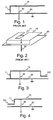
- Fig. 1 illustrates such a microstrip antenna in cross section.
- Fig. 1 shows a ground plane 20, radiator 10 and a feed line 30.
- the radiator 10 is short-circuited at its first end to the ground plane 20 through a short-circuiting part 11.
- the second end of the radiator is open.
- Fig. 1 does not specifically show the dielectric medium which may be air, for example.
- Microstrip antennas are often implemented on printed circuit boards, in which case there is the usual dielectric pcb material between the radiator 10 and ground plane 20.
- a typical problem with planar antenna constructions according to the prior art is their thickness and narrow band.
- Antennas used in personal mobile communications devices must be small in size.
- making the microstrip antenna thinner makes the usable frequency band of the antenna narrower.
- Many mobile communications systems require a relatively wide frequency band, e.g. the DCS-1800 system requires a 10% frequency band, approximately, relative to the center frequency.
- the transmit and receive bands are spaced at 45 MHz from each other, the transmit band being 890-915 MHz and the receive band 935-960 MHz.
- the frequency band should be considerably wide, at least 890-960 MHz in the case of GSM. Because of manufacturing tolerances and objects near the antenna, such as e.g. the hand of the user, which affect the resonance frequency, the bandwidth must be even wider than in the ideal case.
- a second approach is to realize an antenna with two frequency bands such that the first frequency band corresponds to the transmit band and the second frequency band corresponds to the receive band.
- the frequency bands of the antenna need not be as wide as those of a single-band antenna.
- Such dual-band antennas may comprise e.g. two helix antennas tuned to different frequencies or a combination of a rod antenna and a helix, where the rod and helix are tuned to different frequency ranges.
- Such constructions are described e.g. in Finnish patent application no. 952780.
- Such helix antenna constructions are difficult to realize inside the housing of a mobile communications device.
- these arrangements only operate on two frequency bands.
- future multimode mobile communications devices operating in more than one mobile communications system require antenna constructions operating in more than two separate frequency bands.
- Microstrip constructions can be used to realize many different antenna solutions, say, constructions with more than one operating band.
- Fig. 2 shows an example of such a construction.
- Fig. 2 shows a ground plane 20, radiator 10 and a feed line 30.
- a gap 15 divides the radiator 10 in two parts having different resonance frequencies.
- the radiator may also have more gaps and more parts in which case there are several resonance frequencies as well.
- Planar dual-band antenna constructions are disclosed e.g. in US patent publication no. 5,124,733.
- Said patent publication discloses a microstrip antenna construction which has in addition to a ground plane one active radiating element and a second passive element.
- the elements are quarter-wave elements short-circuited to the ground plane through one edge.
- the elements have differing resonance frequencies so that the antenna construction has two separate operating frequency bands.
- a disadvantage of such a solution is the thickness of the two stacked antenna elements. Furthermore, this solution, too, allows for operation on two frequency bands only.
- Fig. 2 shows only one feed line 30. It is also known to use more than one feed point and feed line so that the properties of the antenna, such as the resonance frequency, directivity and diversity characteristics, for instance, can be influenced by choosing the feed point used.
- the characteristics of the antenna construction can also be influenced by the shape and size of the radiator in the antenna construction and by the size difference and distance between the radiator and ground plane, for example.
- An object of the invention is to provide an antenna construction which is adaptable and modifiable in many ways. Another object of the invention is provide said antenna construction which is also simple to manufacture. A further object of the invention is to provide an antenna construction the characteristics of which can be electronically controlled during operation.
- the objects of the invention are achieved by realizing a microstrip antenna construction having a matching element capacitively coupled to the ground plane.
- the characteristics of the antenna construction can be controlled in a very versatile manner by controlling the strength of the capacitive coupling of the matching element and the location of the matching element.
- the antenna construction according to the invention is characterized by what is expressed in the characterizing part of the independent claim directed to the antenna construction.
- the mobile communications device according to the invention is characterized by what is expressed in the characterizing part of the independent claim directed to the mobile communications device.
- Other preferred embodiments of the invention are disclosed in the dependent claims.
- the antenna construction according to the invention has a radiator, ground plane and at least one matching element.
- the matching element is capacitively coupled to a ground potential.
- the characteristics of the antenna construction such as the number of resonance frequencies, resonance frequencies and the radiator impedance at the feed point, can be controlled in a very versatile manner by controlling the number and location and the strength of the capacitive coupling of the matching elements.
- Fig. 3 illustrates the antenna construction according to a preferred embodiment of the invention.
- Fig. 3 shows a ground plane 20, radiator 10, short-circuiting part 11 that short-circuits the radiator to the ground plane, and a feed line 30.
- the matching element may be produced e.g. by bending a portion of the radiator 10, in this case the open end, towards the ground plane, whereby the capacitive coupling between the matching element and ground plane is stronger than in other parts of the radiator.
- the capacitive coupling between the matching element and ground plane can be adjusted e.g. by varying the distance between the matching element and ground plane and by varying the matching element area.
- the characteristics of the radiator and thus the whole antenna construction can be varied in many different ways.
- the capacitance of the matching element can be chosen e.g. through experimentation such that the resonance frequency or bandwidth or some other property of the antenna construction, such as the radiator impedance at the feed point, for example, are as desired.
- the matching element can be dimensioned such that the radiator will have a voltage maximum at the matching element whereby the matching element corresponds to an open end or edge of the radiator.
- a matching element 100 at the open end of the radiator increases the capacitance at the open end of the antenna, thus decreasing the resonance frequency of the antenna.
- the capacitance of the matching element 100 placed at the open end of the radiator strongly influences the resonance frequency of the antenna so that the resonance frequency of the antenna may be advantageously controlled using, in addition to the matching element, a capacitive element, such as e.g. a capacitance diode, coupled to the matching element, which capacitive element has a narrow capacitance adjustment range, yet achieves a considerable resonance frequency adjustment range.
- Fig. 4 illustrates a second preferred embodiment of the invention.
- Fig. 4 shows a ground plane 20, radiator 10 and a feed line 30.
- a matching element 100 is placed at the closed end of the radiator.
- the part 11 that connects the closed end of the radiator to the ground plane is connected to the ground plane through the matching element 100.
- the matching element 100 facilitates a tapping-like coupling to the ground plane, i.e. a current maximum can be created at the matching element.
- a matching element 100 placed at the closed end of the radiator increases the inductiveness of the radiator so that the radiator will resonate at 1 ⁇ 4 wavelength instead of 1 ⁇ 2 wavelength.
- the antenna construction may have more than one matching element 100.
- Matching elements may be located at all sides of the radiator. A given side may also have more than one matching element.
- Fig. 5a illustrates a preferred embodiment of the invention in which a radiator 10 is coupled through a matching element to a separate conductive patch 25 which is capacitively coupled to the ground plane 20 proper.
- the coupling of the separate conductive patch to the ground plane can be realized using a fixed capacitance element or variable capacitance element 26 such as a varactor.
- the capacitance element 26 may also be realized by means of a combination of one or more fixed and one or more variable capacitive elements, such as e.g. a fixed capacitor and a varactor.
- the separate conductive patch may be realized e.g. as an electrically conductive pattern on a printed circuit board. Such a separate conductive patch makes it possible to control the coupling of the matching element to the ground plane in a versatile manner.
- Fig. 5a also shows a feed line 30.
- ground plane 20 and the separate conductive patch 25 may be coupled to each other by means of a switching element, such as e.g. a PIN diode or FET transistor, in addition to or instead of capacitance elements.
- a switching element such as e.g. a PIN diode or FET transistor
- Fig. 5b illustrates a preferred embodiment of the invention in which a radiator 10 is coupled through a matching element 100 to both the ground plane 20 and separate conductive patch 25, which in turn is capacitively coupled to the ground plane 20 through a capacitance element 26.
- One and the same matching element may thus be coupled to both the ground plane and the separate conductive patch.
- one and the same matching element may be coupled to more than one separate conductive patch.
- Fig. 5b also shows a feed line 30.
- Fig. 6 shows a preferred embodiment of the invention that utilizes matching lines 120.
- matching lines 120 are used to galvanically connect a matching element 100 to a separate conductive patch 25 which in turn is connected through a capacitive element 26 to the ground plane.
- the matching element 100 also extends in between the radiator 10 and ground plane 20 whereby the matching element 100 is coupled to the ground plane 20 twice: capacitively directly from the matching element to the ground plane and via the matching lines 120, separate conductive patch 25 and capacitive element 26.
- the characteristics of the antenna construction are influenced e.g. by the dimensions of the matching lines 120 and capacitive element 26 as well as by the distance between the matching element 100 and ground plane.
- Fig. 6 also shows a feed line 30.
- Fig. 7 shows a second example of a preferred embodiment of the invention that utilizes matching lines 120.
- the matching lines 120 galvanically connect a matching element 100 to a separate conductive patch 25 which in turn is connected through a capacitive element 26 to the ground plane.
- the matching element 100 is coupled to the ground plane 20 twice: via the matching lines 120, separate conductive patch 25 and capacitive element 26 as well as via a second separate conductive patch 25b and capacitive element 26b.
- the characteristics of the antenna construction are influenced e.g. by the dimensions of the matching lines 120 and capacitive elements 26, 26b as well as by the distance between the matching element 100 and the second separate conductive patch 25b.
- Fig. 7 also shows a feed line 30 and radiator 10. As illustrated by the example of Fig. 7, different embodiments of the invention may use more than one separate conductive patch 25, 25b, say, two or more separate conductive patches.
- the matching element 100 may also comprise a plurality of parts.
- Fig. 8 illustrates such an embodiment.
- the matching element 100, 100b is comprised of two parts connected by a switching element 130.
- the coupling between the matching element parts 100, 100b may also be realized e.g. by means of a spring, friction or crimp coupling instead of a separate switching element 130.
- Matching element part 100b, which is separate from the antenna 100, 10 proper, may be placed in various locations at the mobile communications device, say, on the body, printed circuit board or battery module of the mobile communications device.
- Such an embodiment allows for various structural solutions as the different parts of the antenna construction may be attached to different structural entities.
- a matching element may also comprise more than two parts connected to each other through a switching element.
- the strength of the capacitive coupling between the matching element and ground plane is also influenced by the quantity of matching element parts connected together at any one time.
- Such an embodiment advantageously uses an electronic switching element, such as a FET transistor, for example, as the switching element 130, whereby the characteristics of the antenna construction can be controlled by software, say, by the control unit of the mobile communications device.
- Fig. 9 illustrates the structure of a matching element 100 according to a preferred embodiment of the invention.
- the matching element 100 faces the separate conductive patch 25 only at a certain point so that the capacitive coupling between the matching element and conductive patch 25 is realized only at that point.
- the matching element may also be above the ground plane 20 at a certain point.
- Fig. 9 also illustrates a design of the matching element 100 parallel to the ground plane and a design perpendicular to the ground plane.
- Fig. 9 also shows a radiator 10, ground plane 20, feed line 30 and a capacitive element 26 that couples the separate conductive patch to the ground plane.
- the matching element 100 may also be designed in many other ways than those described in the examples above.
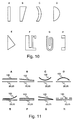
- Fig. 10 illustrates examples of matching element shapes according to various embodiments of the invention.
- the matching element may be e.g. rectangular or square, as in examples A and B in Fig. 10, or curved or semicircular as in examples C and D.
- the matching element may also be triangular as in example E. Also more complex combinations of differently shaped strips, rectangles and curves are advantageous, as shown in examples F, G and H in Fig. 10.
- Example F in Fig. 10 is well suited e.g. to an embodiment in which one and the same matching element is used for coupling to two different targets such as e.g. two separate conductive patches or ground plane and a separate conductive patch.
- Some examples of Fig. 10 show in broken lines sides of the matching element that are particularly suitable for attaching the matching element to the radiator.
- Fig. 11 illustrates, perpendicular to the ground plane, cross sections of matching elements according to preferred embodiments of the invention.
- the matching element 100 may be parallel to the ground plane 20 or separate conductive patch 25 according to example A in Fig. 11, or divergent, as in example B.
- the matching element 100 may also be designed curved, the convex side facing the ground plane 20 or separate conductive patch 25 as in example C, or the concave side facing the ground plane 20 or separate conductive patch 25 as in example D. Combinations of the basic shapes are also possible, as illustrated by example E.
- Examples F and G in Fig. 11 illustrate a situation where the matching element is galvanically connected to the ground plane 20 or separate conductive patch 25.
- connection may be realized using a matching line, as depicted by example F, or the matching element 100 may extend without a separate matching line to the ground plane 20 or separate conductive patch 25, as illustrated by example G.
- the matching element 100 may also be comprised of several parts in accordance with example H.
- the antenna construction according to the invention finds particular utility in mobile communications devices.
- the antenna construction can be placed in a mobile communications device in many different ways. Below are described some examples of the placement of the antenna construction according to the invention in a mobile communications device. It should be noted that these embodiments are just illustrative examples and do not in any way limit the different implementations of the antenna construction according to the invention.
- a problem with mobile communications devices is the lack of space available. This affects particularly the design of antenna constructions in mobile communications devices.
- the antenna of a mobile communications device is typically placed at the rear of the device, away from the user.
- the battery of the mobile communications device is also placed at the rear side of the device because the front side is needed to realize a user interface, i.e. a keypad and a display.
- the battery is typically realized as a removable battery module so that the user can easily replace the battery.
- the battery module limits the rear area available to the antenna of the mobile communications device.
- at least part of the antenna construction of the mobile communications device is placed in the battery module of the mobile communications device. Such an embodiment makes possible better optimization of the space usage.
- the embodiment is particularly advantageous in connection with antenna constructions according to the invention for in many different embodiments of the invention the matching elements add to the area required by the antenna construction.
- Fig. 12a illustrates the structure of a battery module 350 according to a preferred embodiment of the invention.
- the battery module comprises battery cells 360 and components, such as electronic control elements and connectors 355, related to the battery module functions.
- the battery module also comprises a radiator 10 and matching element 100.
- the placement of the parts of the antenna construction in the battery module makes it possible to utilize the optimization possibilities achieved by means of changes in the internal structure of the battery module.
- the battery cells are relatively large components so that space is easily left between the antenna construction and a battery cell, which space can be utilized for the placement of other components 355 in the battery module.
- the internal structure of the battery module thus facilitates many different modifications.
- the structure of Fig. 12a is just one example of a possible structure and does not limit the different implementations of the invention in any way.
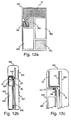
- Fig. 12b illustrates a second preferred embodiment of the invention where part of the antenna construction is in the battery module.
- Fig. 12b shows a mobile communications device 300 comprising a user interface, in this example a display 306 and keypad 307, on the front side of the mobile communications device.
- the mobile communications device also comprises a printed circuit board 330 which has a ground plane 20 and a separate conductive patch 25 realized by means of electrically conductive patterns.
- the mobile communications device comprises other components as well, but for simplicity these are not shown in Fig. 12b.
- the mobile communications device includes a battery module 350 which in this example comprises a battery cell 360, radiator 10 and a matching element 100 attached to the radiator.
- Antenna feed is realized through a connector 351 from the mobile communications device to the battery module and further to the radiator.
- the ground plane 20 of the antenna construction is located at the mobile communications device side, on its printed circuit board 330.
- the matching element 100 is realized in such a manner that its distance from the separate conductive patch 25 is smaller than the distance between the radiator 10 and ground plane 20, whereby the capacitive coupling between the matching element and separate conductive patch is weaker than that between the radiator and ground plane.
- Fig. 12c illustrates a third preferred embodiment of the invention where part of the antenna construction is located in the battery module 350.
- the ground plane 20, radiator 10 and separate conductive patch 25 of the antenna construction are located on the side of the mobile communications device and the matching element 100 on the side of the battery module 350.
- the radiator 10 and matching element are galvanically connected to each other through contact 101.
- Fig. 12c also shows a printed circuit board 330 and battery cell 360 in the mobile communications device.
- the antenna construction according to the invention finds utility in mobile stations of many different cellular systems and in small base stations.
- the antenna construction according to the invention is applicable in mobile communications devices of the GSM and UMTS systems.
- the antenna construction according to the invention finds particular utility in applications where the mobile communications device must be able to monitor more than one frequency range, such as e.g. mobile communications devices operating in both the GSM 900 and GSM 1800 systems.
- the antenna construction according to the invention is also applicable to other compact radio apparatus, such as base stations of wireless intercom systems and mobile communication systems based on micro- and picocell networks.
- the controllability of the antenna construction according to the invention as well as the great number of frequency range options provided by the antenna construction makes the use of the antenna construction according to the invention particularly advantageous also in forthcoming software radio systems, where the frequency ranges and radio interface functions such as modulations used, are selected by software so that the mobile station can be adapted to another mobile communication system just by changing the software at the mobile station.
- a matching element according to the invention can be used for controlling many different properties of an antenna construction.
- the matching element can be used e.g. to influence the directivity of the antenna construction or its diversity characteristics as well as its resonance frequency or frequencies and the quantity of the resonance frequencies, the bandwidth of each resonance band or e.g. the largest continuous bandwidth of the antenna construction.
- the matching element can be used to influence the impedance of the feed point.
- the matching element according to the invention can be realized in many different ways according to the application in question.
- the matching element can be implemented by having a projection of a desired shape in the radiator and bending said projection in the vicinity of the ground plane or separate conductive patch.
- the matching element may also be realized in many other ways, say, by soldering, crimping or otherwise attaching the matching element to the radiator.
- the radiator is implemented using a conductive pattern on a printed circuit board
- the matching element can be realized on the other side of the printed circuit board or by means of a conductive pattern formed on an intermediate layer of a multilayer board.
- the matching element may be connected to the radiator using conventional pcb manufacturing techniques, e.g. by means of one or more metal-plated through holes.
- the antenna construction according to the invention has many advantages.
- the antenna construction according to the invention is simple to manufacture, yet provides a wide range of control for the characteristics of the antenna construction. Matching elements placed in different locations of the radiator can be used to control a great number of properties of the antenna construction.
- the antenna construction according to the invention thus facilitates versatile control options during the manufacture of the antenna construction.
- the antenna construction according to the invention makes it possible to control the characteristics of the antenna construction also during the use of the antenna construction, e.g. by using a varactor to vary the strength of the capacitive coupling between the matching element and ground plane. This way, a mobile communications device can control e.g. the resonance frequency of the antenna in accordance with the communications frequency used.
- the antenna construction according to the invention has the advantage of being applicable to reduce the effect of external lossy materials, such as other parts of the mobile communications device or materials outside the mobile communications device such as the hand of the user, on the resonance frequency of the antenna construction.
- the resonance frequency of the antenna decreases as a lossy material affects the radiator and antenna ground plane at the same time.
- the matching element 100 or matching elements 100 of the antenna construction according to the invention strengthen the coupling between the radiator and ground plane, whereby the coupling between the mobile communications device body or materials outside the body and the antenna construction becomes relatively weaker.
- the effect of the mobile communications device body or materials outside the body on the resonance frequency of the antenna construction is smaller than in antenna constructions according to the prior art.
Landscapes
- Engineering & Computer Science (AREA)
- Computer Networks & Wireless Communication (AREA)
- Waveguide Aerials (AREA)
- Support Of Aerials (AREA)
Applications Claiming Priority (2)
| Application Number | Priority Date | Filing Date | Title |
|---|---|---|---|
| FI991068 | 1999-05-10 | ||
| FI991068A FI113588B (fi) | 1999-05-10 | 1999-05-10 | Antennirakenne |
Publications (3)
| Publication Number | Publication Date |
|---|---|
| EP1052723A2 true EP1052723A2 (fr) | 2000-11-15 |
| EP1052723A3 EP1052723A3 (fr) | 2002-03-27 |
| EP1052723B1 EP1052723B1 (fr) | 2005-10-12 |
Family
ID=8554633
Family Applications (1)
| Application Number | Title | Priority Date | Filing Date |
|---|---|---|---|
| EP00660084A Expired - Lifetime EP1052723B1 (fr) | 1999-05-10 | 2000-05-08 | Structure d'antenne |
Country Status (4)
| Country | Link |
|---|---|
| US (1) | US6297776B1 (fr) |
| EP (1) | EP1052723B1 (fr) |
| DE (1) | DE60023062T2 (fr) |
| FI (1) | FI113588B (fr) |
Cited By (42)
| Publication number | Priority date | Publication date | Assignee | Title |
|---|---|---|---|---|
| WO2001089031A1 (fr) * | 2000-05-15 | 2001-11-22 | Avantego Ab | Dispositif d'antenne |
| GB2367189A (en) * | 2000-08-17 | 2002-03-27 | Nec Corp | Portable communication unit and internal antenna therefor |
| WO2002054534A1 (fr) * | 2000-12-29 | 2002-07-11 | Allgon Mobile Communications Ab | Ensemble antenne |
| EP1209760A3 (fr) * | 2000-11-22 | 2003-02-26 | Matsushita Electric Industrial Co., Ltd. | Antenne incorporée pour un appareil de radiotéléphonie |
| WO2003069728A1 (fr) * | 2002-02-14 | 2003-08-21 | Ericsson, Inc. | Antennes comportant de multiples bandes de frequences de resonance et terminaux sans fil incorporant de telles antennes |
| EP1263083A3 (fr) * | 2001-06-01 | 2004-01-21 | Matsushita Electric Industrial Co., Ltd. | Antenne en F inversée et appareil portable de communication incorporant une telle antenne |
| EP1211750A3 (fr) * | 2000-11-30 | 2004-02-04 | Kabushiki Kaisha Toshiba | Dispositif radio à une antenne |
| EP1396906A1 (fr) * | 2002-08-30 | 2004-03-10 | Filtronic LK Oy | Antenne planaire multibandes accordable |
| WO2004062032A1 (fr) * | 2002-12-17 | 2004-07-22 | Sony Ericsson Mobile Communications Ab | Antennes planes a frequences de resonance multiples |
| EP1116299A4 (fr) * | 1999-07-21 | 2004-09-29 | Rangestar Wireless Inc | Structure d'antenne large bande a accord capacitif |
| EP1469549A1 (fr) * | 2003-04-15 | 2004-10-20 | Filtronic LK Oy | Antenne multibande ajustable de type PIFA |
| EP1490925A4 (fr) * | 2002-03-05 | 2005-06-01 | Prec Dynamics Corp | Antenne microruban pour element d'identification |
| EP1542313A1 (fr) * | 2003-12-11 | 2005-06-15 | Nec Corporation | Dispositif d'antenne comportant un circuit d'adaption d'impédance variable et appareil de radiocommunication portatif utilisant cette antenne |
| EP1544943A1 (fr) * | 2003-12-15 | 2005-06-22 | Filtronic LK Oy | Antenne planaire multibandes accordable |
| US6980154B2 (en) | 2003-10-23 | 2005-12-27 | Sony Ericsson Mobile Communications Ab | Planar inverted F antennas including current nulls between feed and ground couplings and related communications devices |
| EP1619751A1 (fr) * | 2004-07-23 | 2006-01-25 | EADS Deutschland GmbH | Antenne à large bande et à profil bas |
| WO2006042562A1 (fr) * | 2004-10-23 | 2006-04-27 | Electronics Research Institute | Antenne quadband compacte a alimentation unique destinee a des systemes de communication sans fil |
| EP1209759B1 (fr) * | 2000-11-22 | 2006-05-31 | Matsushita Electric Industrial Co., Ltd. | Antenne et dispositif sans fil avec une telle antenne |
| EP1662606A1 (fr) * | 2004-11-24 | 2006-05-31 | Samsung Electronics Co., Ltd. | Antenne intégrée pour appareil radio portable |
| EP1624588A4 (fr) * | 2003-05-14 | 2006-07-05 | Mitsubishi Electric Corp | Radio portable |
| WO2007012697A1 (fr) * | 2005-07-25 | 2007-02-01 | Pulse Finland Oy | Antenne multibande reglable |
| WO2007019855A1 (fr) * | 2005-08-12 | 2007-02-22 | Gn Netcom A/S | Unité de communication avec antenne intégrée |
| WO2007040638A1 (fr) * | 2005-09-29 | 2007-04-12 | Sony Ericsson Mobile Communications Ab | Antenne monopôle courbe multibande |
| EP1816703A4 (fr) * | 2004-11-29 | 2007-11-28 | Matsushita Electric Industrial Co Ltd | Dispositif d'antenne |
| WO2008084273A3 (fr) * | 2006-12-21 | 2008-12-04 | Nokia Corp | Dispositif d'antenne |
| WO2009037353A1 (fr) * | 2007-09-20 | 2009-03-26 | Nokia Corporation | Système d'antenne, procédé de production d'un système d'antenne et carte imprimée destinée à être utilisée dans un système d'antenne |
| EP2120287A1 (fr) * | 2008-05-16 | 2009-11-18 | Laird Technologies AB | Dispositif d'antenne |
| WO2010006819A1 (fr) * | 2008-07-18 | 2010-01-21 | Sony Ericsson Mobile Communications Ab | Agencement d'antenne |
| US7679565B2 (en) | 2004-06-28 | 2010-03-16 | Pulse Finland Oy | Chip antenna apparatus and methods |
| WO2010029306A1 (fr) * | 2008-09-12 | 2010-03-18 | The University Of Birmingham | Antenne multifonctionnelle |
| US7786938B2 (en) | 2004-06-28 | 2010-08-31 | Pulse Finland Oy | Antenna, component and methods |
| US7821470B2 (en) | 2008-07-18 | 2010-10-26 | Sony Ericsson Mobile Communications Ab | Antenna arrangement |
| US7903035B2 (en) | 2005-10-10 | 2011-03-08 | Pulse Finland Oy | Internal antenna and methods |
| CN102084541A (zh) * | 2008-05-02 | 2011-06-01 | 北方电讯网络有限公司 | 低轮廓、宽带宽射频天线 |
| US8108021B2 (en) | 2010-05-27 | 2012-01-31 | Sony Ericsson Mobile Communications Ab | Communications structures including antennas with filters between antenna elements and ground sheets |
| EP2169839A3 (fr) * | 2008-09-29 | 2012-10-10 | TDK Corporation | Transmetteur radio |
| US8456366B2 (en) | 2010-04-26 | 2013-06-04 | Sony Corporation | Communications structures including antennas with separate antenna branches coupled to feed and ground conductors |
| EP2846398A3 (fr) * | 2013-08-13 | 2015-07-01 | Fujitsu Limited | Appareil d'antenne |
| US9673507B2 (en) | 2011-02-11 | 2017-06-06 | Pulse Finland Oy | Chassis-excited antenna apparatus and methods |
| US9917346B2 (en) | 2011-02-11 | 2018-03-13 | Pulse Finland Oy | Chassis-excited antenna apparatus and methods |
| US10211538B2 (en) | 2006-12-28 | 2019-02-19 | Pulse Finland Oy | Directional antenna apparatus and methods |
| EP2688141B1 (fr) * | 2012-07-19 | 2020-01-01 | BlackBerry Limited | Procédé et appareil de formation de faisceau et d'accord d'antenne dans un dispositif de communication |
Families Citing this family (69)
| Publication number | Priority date | Publication date | Assignee | Title |
|---|---|---|---|---|
| FI113911B (fi) * | 1999-12-30 | 2004-06-30 | Nokia Corp | Menetelmä signaalin kytkemiseksi ja antennirakenne |
| GB0013156D0 (en) * | 2000-06-01 | 2000-07-19 | Koninkl Philips Electronics Nv | Dual band patch antenna |
| AU8007601A (en) * | 2000-08-28 | 2002-03-13 | In4Tel Ltd | Apparatus and method for enhancing low-frequency operation of mobile communication antennas |
| WO2002039538A2 (fr) * | 2000-10-20 | 2002-05-16 | Rangestar Wireless, Inc. | Antenne compacte a polarisations multiples |
| GB0105441D0 (en) * | 2001-03-03 | 2001-04-25 | Koninkl Philips Electronics Nv | Antenna arrangement |
| TW579077U (en) * | 2001-04-11 | 2004-03-01 | Wistron Neweb Corp | Tunable antenna for radio transceiver device |
| JP2002353731A (ja) * | 2001-05-15 | 2002-12-06 | Z-Com Inc | 逆fアンテナとその製造方法 |
| EP1942551A1 (fr) * | 2001-10-16 | 2008-07-09 | Fractus, S.A. | Antenne multibande |
| US7050004B2 (en) * | 2002-03-28 | 2006-05-23 | University Of Manitoba | Multiple frequency antenna |
| US6714162B1 (en) * | 2002-10-10 | 2004-03-30 | Centurion Wireless Technologies, Inc. | Narrow width dual/tri ISM band PIFA for wireless applications |
| KR100960570B1 (ko) * | 2003-01-06 | 2010-06-03 | 삼성전자주식회사 | 휴대용 컴퓨터 |
| TW558084U (en) * | 2003-03-07 | 2003-10-11 | Hon Hai Prec Ind Co Ltd | Multi-band antenna |
| TW562258U (en) * | 2003-04-04 | 2003-11-11 | Z Com Inc | Structure of 3D inverted F-antenna |
| US6819290B2 (en) * | 2003-04-08 | 2004-11-16 | Motorola Inc. | Variable multi-band planar antenna assembly |
| US6850200B2 (en) * | 2003-06-13 | 2005-02-01 | Motorola, Inc. | Compact PIFA antenna for automated manufacturing |
| FR2869727B1 (fr) * | 2004-04-30 | 2007-04-06 | Get Enst Bretagne Etablissemen | Antenne planaire a plots conducteurs s'etendant a partir du plan de masse et/ou d'au moins un element rayonnant, et procede de fabrication correspondant |
| US7345634B2 (en) * | 2004-08-20 | 2008-03-18 | Kyocera Corporation | Planar inverted “F” antenna and method of tuning same |
| JP4306580B2 (ja) * | 2004-10-13 | 2009-08-05 | 日立電線株式会社 | 2周波共用フィルムアンテナ |
| FI119009B (fi) | 2005-10-03 | 2008-06-13 | Pulse Finland Oy | Monikaistainen antennijärjestelmä |
| FI118782B (fi) | 2005-10-14 | 2008-03-14 | Pulse Finland Oy | Säädettävä antenni |
| US7479927B2 (en) * | 2005-12-30 | 2009-01-20 | Motorola, Inc. | Radio frequency antenna system |
| US7633446B2 (en) * | 2006-02-22 | 2009-12-15 | Mediatek Inc. | Antenna apparatus and mobile communication device using the same |
| US8618990B2 (en) | 2011-04-13 | 2013-12-31 | Pulse Finland Oy | Wideband antenna and methods |
| US7492318B2 (en) * | 2007-02-15 | 2009-02-17 | Laird Technologies, Inc. | Mobile wideband antennas |
| FI20075269A0 (fi) | 2007-04-19 | 2007-04-19 | Pulse Finland Oy | Menetelmä ja järjestely antennin sovittamiseksi |
| FI120427B (fi) | 2007-08-30 | 2009-10-15 | Pulse Finland Oy | Säädettävä monikaista-antenni |
| US8446322B2 (en) * | 2007-11-29 | 2013-05-21 | Topcon Gps, Llc | Patch antenna with capacitive elements |
| JP4387441B1 (ja) * | 2008-07-29 | 2009-12-16 | 株式会社東芝 | アンテナ装置および電子機器 |
| US20100194654A1 (en) * | 2009-02-03 | 2010-08-05 | Chi-Ming Chiang | Antenna structure with an effect of capacitance in serial connecting |
| FI20096134A0 (fi) | 2009-11-03 | 2009-11-03 | Pulse Finland Oy | Säädettävä antenni |
| TWI448006B (zh) * | 2009-11-20 | 2014-08-01 | Arcadyan Technology Corp | 具多頻帶之天線 |
| FI20096251A0 (sv) | 2009-11-27 | 2009-11-27 | Pulse Finland Oy | MIMO-antenn |
| US8847833B2 (en) | 2009-12-29 | 2014-09-30 | Pulse Finland Oy | Loop resonator apparatus and methods for enhanced field control |
| FI20105158L (fi) | 2010-02-18 | 2011-08-19 | Pulse Finland Oy | Kuorisäteilijällä varustettu antenni |
| US8390520B2 (en) * | 2010-03-11 | 2013-03-05 | Raytheon Company | Dual-patch antenna and array |
| US9406998B2 (en) | 2010-04-21 | 2016-08-02 | Pulse Finland Oy | Distributed multiband antenna and methods |
| IT1400110B1 (it) * | 2010-05-21 | 2013-05-17 | S Di G Moiraghi & C Soc Sa | Antenna planare compatta. |
| FI20115072A0 (fi) | 2011-01-25 | 2011-01-25 | Pulse Finland Oy | Moniresonanssiantenni, -antennimoduuli ja radiolaite |
| US8866689B2 (en) | 2011-07-07 | 2014-10-21 | Pulse Finland Oy | Multi-band antenna and methods for long term evolution wireless system |
| US9450291B2 (en) | 2011-07-25 | 2016-09-20 | Pulse Finland Oy | Multiband slot loop antenna apparatus and methods |
| US9123990B2 (en) | 2011-10-07 | 2015-09-01 | Pulse Finland Oy | Multi-feed antenna apparatus and methods |
| US9531058B2 (en) | 2011-12-20 | 2016-12-27 | Pulse Finland Oy | Loosely-coupled radio antenna apparatus and methods |
| US9484619B2 (en) | 2011-12-21 | 2016-11-01 | Pulse Finland Oy | Switchable diversity antenna apparatus and methods |
| US8988296B2 (en) | 2012-04-04 | 2015-03-24 | Pulse Finland Oy | Compact polarized antenna and methods |
| US9979078B2 (en) | 2012-10-25 | 2018-05-22 | Pulse Finland Oy | Modular cell antenna apparatus and methods |
| US10069209B2 (en) | 2012-11-06 | 2018-09-04 | Pulse Finland Oy | Capacitively coupled antenna apparatus and methods |
| KR101372140B1 (ko) * | 2013-01-25 | 2014-03-07 | 엘지이노텍 주식회사 | 안테나 장치 및 그의 급전 구조체 |
| US10079428B2 (en) | 2013-03-11 | 2018-09-18 | Pulse Finland Oy | Coupled antenna structure and methods |
| US9647338B2 (en) | 2013-03-11 | 2017-05-09 | Pulse Finland Oy | Coupled antenna structure and methods |
| US9634383B2 (en) | 2013-06-26 | 2017-04-25 | Pulse Finland Oy | Galvanically separated non-interacting antenna sector apparatus and methods |
| US9680212B2 (en) | 2013-11-20 | 2017-06-13 | Pulse Finland Oy | Capacitive grounding methods and apparatus for mobile devices |
| CN110085994B (zh) * | 2013-11-22 | 2021-08-20 | 华为终端有限公司 | 一种可调天线及终端 |
| US9590308B2 (en) | 2013-12-03 | 2017-03-07 | Pulse Electronics, Inc. | Reduced surface area antenna apparatus and mobile communications devices incorporating the same |
| US9350081B2 (en) | 2014-01-14 | 2016-05-24 | Pulse Finland Oy | Switchable multi-radiator high band antenna apparatus |
| US9496601B1 (en) | 2014-01-16 | 2016-11-15 | Google Inc. | Antenna assembly utilizing space between a battery and a housing |
| US9948002B2 (en) | 2014-08-26 | 2018-04-17 | Pulse Finland Oy | Antenna apparatus with an integrated proximity sensor and methods |
| US9973228B2 (en) | 2014-08-26 | 2018-05-15 | Pulse Finland Oy | Antenna apparatus with an integrated proximity sensor and methods |
| US9722308B2 (en) | 2014-08-28 | 2017-08-01 | Pulse Finland Oy | Low passive intermodulation distributed antenna system for multiple-input multiple-output systems and methods of use |
| US9906260B2 (en) | 2015-07-30 | 2018-02-27 | Pulse Finland Oy | Sensor-based closed loop antenna swapping apparatus and methods |
| US10826182B2 (en) * | 2016-10-12 | 2020-11-03 | Carrier Corporation | Through-hole inverted sheet metal antenna |
| US20180175493A1 (en) * | 2016-12-15 | 2018-06-21 | Nanning Fugui Precision Industrial Co., Ltd. | Antenna device and electronic device using the same |
| JP6842040B2 (ja) * | 2017-03-15 | 2021-03-17 | ミツミ電機株式会社 | アンテナ装置及びその製造方法 |
| WO2020173292A1 (fr) | 2019-02-27 | 2020-09-03 | 华为技术有限公司 | Appareil d'antenne et dispositif électronique |
| CN111628274B (zh) * | 2019-02-27 | 2022-10-04 | 华为技术有限公司 | 天线装置及电子设备 |
| US10992025B2 (en) | 2019-04-12 | 2021-04-27 | Verily Life Sciences Llc | Antenna with extended range |
| JP7298505B2 (ja) * | 2020-02-19 | 2023-06-27 | 株式会社デンソー | アンテナ装置 |
| TWI732691B (zh) * | 2020-09-30 | 2021-07-01 | 華碩電腦股份有限公司 | 立體電子構件及電子裝置 |
| EP4002589B1 (fr) | 2020-11-24 | 2026-02-25 | Nokia Solutions and Networks Oy | Système d'antenne |
| CN117810674A (zh) * | 2022-09-30 | 2024-04-02 | Oppo广东移动通信有限公司 | 天线组件及电子设备 |
Family Cites Families (9)
| Publication number | Priority date | Publication date | Assignee | Title |
|---|---|---|---|---|
| JPH03263903A (ja) | 1989-04-28 | 1991-11-25 | Misao Haishi | 小形アンテナ |
| JP3326935B2 (ja) * | 1993-12-27 | 2002-09-24 | 株式会社日立製作所 | 携帯無線機用小型アンテナ |
| SE507077C2 (sv) * | 1996-05-17 | 1998-03-23 | Allgon Ab | Antennanordning för en portabel radiokommunikationsanordning |
| US5764190A (en) * | 1996-07-15 | 1998-06-09 | The Hong Kong University Of Science & Technology | Capacitively loaded PIFA |
| JP3384524B2 (ja) * | 1996-09-19 | 2003-03-10 | 株式会社エヌ・ティ・ティ・ドコモ | マイクロストリップアンテナ装置 |
| US6008762A (en) * | 1997-03-31 | 1999-12-28 | Qualcomm Incorporated | Folded quarter-wave patch antenna |
| JP3286912B2 (ja) * | 1997-12-19 | 2002-05-27 | 株式会社村田製作所 | 表面実装型アンテナおよびそれを用いた通信機 |
| FR2778500B1 (fr) * | 1998-05-05 | 2000-08-04 | Socapex Amphenol | Antenne a plaque |
| FR2791815A1 (fr) * | 1999-04-02 | 2000-10-06 | Rene Liger | Antenne compacte |
-
1999
- 1999-05-10 FI FI991068A patent/FI113588B/fi not_active IP Right Cessation
-
2000
- 2000-05-08 EP EP00660084A patent/EP1052723B1/fr not_active Expired - Lifetime
- 2000-05-08 DE DE60023062T patent/DE60023062T2/de not_active Expired - Lifetime
- 2000-05-09 US US09/567,828 patent/US6297776B1/en not_active Expired - Lifetime
Cited By (69)
| Publication number | Priority date | Publication date | Assignee | Title |
|---|---|---|---|---|
| EP1116299A4 (fr) * | 1999-07-21 | 2004-09-29 | Rangestar Wireless Inc | Structure d'antenne large bande a accord capacitif |
| WO2001089031A1 (fr) * | 2000-05-15 | 2001-11-22 | Avantego Ab | Dispositif d'antenne |
| GB2367189A (en) * | 2000-08-17 | 2002-03-27 | Nec Corp | Portable communication unit and internal antenna therefor |
| GB2367189B (en) * | 2000-08-17 | 2003-01-15 | Nec Corp | Portable communication unit and internal antenna therefor |
| US7483728B2 (en) | 2000-08-17 | 2009-01-27 | Nec Corporation | Portable communication unit and internal antenna used for same |
| US6897814B2 (en) | 2000-11-22 | 2005-05-24 | Matsushita Electric Industrial Co., Ltd. | Mobile radio |
| EP1209760A3 (fr) * | 2000-11-22 | 2003-02-26 | Matsushita Electric Industrial Co., Ltd. | Antenne incorporée pour un appareil de radiotéléphonie |
| EP1209759B1 (fr) * | 2000-11-22 | 2006-05-31 | Matsushita Electric Industrial Co., Ltd. | Antenne et dispositif sans fil avec une telle antenne |
| EP1763106A1 (fr) * | 2000-11-22 | 2007-03-14 | Matsushita Electric Industrial Co., Ltd. | Antenne incorporée pour un appareil de radiotéléphonie |
| EP1211750A3 (fr) * | 2000-11-30 | 2004-02-04 | Kabushiki Kaisha Toshiba | Dispositif radio à une antenne |
| WO2002054534A1 (fr) * | 2000-12-29 | 2002-07-11 | Allgon Mobile Communications Ab | Ensemble antenne |
| US6903688B2 (en) | 2000-12-29 | 2005-06-07 | Amc Centurion Ab | Antenna device |
| EP1263083A3 (fr) * | 2001-06-01 | 2004-01-21 | Matsushita Electric Industrial Co., Ltd. | Antenne en F inversée et appareil portable de communication incorporant une telle antenne |
| US6700540B2 (en) | 2002-02-14 | 2004-03-02 | Ericsson, Inc. | Antennas having multiple resonant frequency bands and wireless terminals incorporating the same |
| WO2003069728A1 (fr) * | 2002-02-14 | 2003-08-21 | Ericsson, Inc. | Antennes comportant de multiples bandes de frequences de resonance et terminaux sans fil incorporant de telles antennes |
| EP1490925A4 (fr) * | 2002-03-05 | 2005-06-01 | Prec Dynamics Corp | Antenne microruban pour element d'identification |
| CN100388558C (zh) * | 2002-03-05 | 2008-05-14 | 精密动力公司 | 用于识别装置的微带天线 |
| US6876329B2 (en) | 2002-08-30 | 2005-04-05 | Filtronic Lk Oy | Adjustable planar antenna |
| EP1396906A1 (fr) * | 2002-08-30 | 2004-03-10 | Filtronic LK Oy | Antenne planaire multibandes accordable |
| US6903686B2 (en) | 2002-12-17 | 2005-06-07 | Sony Ericsson Mobile Communications Ab | Multi-branch planar antennas having multiple resonant frequency bands and wireless terminals incorporating the same |
| WO2004062032A1 (fr) * | 2002-12-17 | 2004-07-22 | Sony Ericsson Mobile Communications Ab | Antennes planes a frequences de resonance multiples |
| EP1469549A1 (fr) * | 2003-04-15 | 2004-10-20 | Filtronic LK Oy | Antenne multibande ajustable de type PIFA |
| US7099690B2 (en) | 2003-04-15 | 2006-08-29 | Lk Products Oy | Adjustable multi-band antenna |
| EP1624588A4 (fr) * | 2003-05-14 | 2006-07-05 | Mitsubishi Electric Corp | Radio portable |
| US6980154B2 (en) | 2003-10-23 | 2005-12-27 | Sony Ericsson Mobile Communications Ab | Planar inverted F antennas including current nulls between feed and ground couplings and related communications devices |
| EP1542313A1 (fr) * | 2003-12-11 | 2005-06-15 | Nec Corporation | Dispositif d'antenne comportant un circuit d'adaption d'impédance variable et appareil de radiocommunication portatif utilisant cette antenne |
| US7176841B2 (en) | 2003-12-11 | 2007-02-13 | Nec Corporation | Antenna device and radio communication apparatus using the antenna device |
| CN100456559C (zh) * | 2003-12-11 | 2009-01-28 | 日本电气株式会社 | 天线设备以及使用该天线设备的无线通信装置 |
| EP1544943A1 (fr) * | 2003-12-15 | 2005-06-22 | Filtronic LK Oy | Antenne planaire multibandes accordable |
| US7468700B2 (en) | 2003-12-15 | 2008-12-23 | Pulse Finland Oy | Adjustable multi-band antenna |
| US7973720B2 (en) | 2004-06-28 | 2011-07-05 | LKP Pulse Finland OY | Chip antenna apparatus and methods |
| US7786938B2 (en) | 2004-06-28 | 2010-08-31 | Pulse Finland Oy | Antenna, component and methods |
| US7679565B2 (en) | 2004-06-28 | 2010-03-16 | Pulse Finland Oy | Chip antenna apparatus and methods |
| US7548204B2 (en) | 2004-07-23 | 2009-06-16 | Eads Deutschland Gmbh | Broadband antenna smaller structure height |
| EP1619751A1 (fr) * | 2004-07-23 | 2006-01-25 | EADS Deutschland GmbH | Antenne à large bande et à profil bas |
| WO2006042562A1 (fr) * | 2004-10-23 | 2006-04-27 | Electronics Research Institute | Antenne quadband compacte a alimentation unique destinee a des systemes de communication sans fil |
| US7433720B2 (en) | 2004-11-24 | 2008-10-07 | Samsung Electronics Co., Ltd | Built-in antenna apparatus of portable wireless terminal |
| EP1662606A1 (fr) * | 2004-11-24 | 2006-05-31 | Samsung Electronics Co., Ltd. | Antenne intégrée pour appareil radio portable |
| US7659793B2 (en) | 2004-11-29 | 2010-02-09 | Panasonic Corporation | Antenna device including a high frequency circuit, a reactance circuit and first and second ground sections |
| EP1816703A4 (fr) * | 2004-11-29 | 2007-11-28 | Matsushita Electric Industrial Co Ltd | Dispositif d'antenne |
| US8564485B2 (en) | 2005-07-25 | 2013-10-22 | Pulse Finland Oy | Adjustable multiband antenna and methods |
| WO2007012697A1 (fr) * | 2005-07-25 | 2007-02-01 | Pulse Finland Oy | Antenne multibande reglable |
| WO2007019855A1 (fr) * | 2005-08-12 | 2007-02-22 | Gn Netcom A/S | Unité de communication avec antenne intégrée |
| WO2007040638A1 (fr) * | 2005-09-29 | 2007-04-12 | Sony Ericsson Mobile Communications Ab | Antenne monopôle courbe multibande |
| US7405701B2 (en) | 2005-09-29 | 2008-07-29 | Sony Ericsson Mobile Communications Ab | Multi-band bent monopole antenna |
| US7903035B2 (en) | 2005-10-10 | 2011-03-08 | Pulse Finland Oy | Internal antenna and methods |
| US8525734B2 (en) | 2006-12-21 | 2013-09-03 | Nokia Corporation | Antenna device |
| WO2008084273A3 (fr) * | 2006-12-21 | 2008-12-04 | Nokia Corp | Dispositif d'antenne |
| US10211538B2 (en) | 2006-12-28 | 2019-02-19 | Pulse Finland Oy | Directional antenna apparatus and methods |
| WO2009037353A1 (fr) * | 2007-09-20 | 2009-03-26 | Nokia Corporation | Système d'antenne, procédé de production d'un système d'antenne et carte imprimée destinée à être utilisée dans un système d'antenne |
| US9692116B2 (en) | 2007-09-20 | 2017-06-27 | Nokia Technologies Oy | Antenna arrangement, a method for manufacturing an antenna arrangement and a printed wiring board for use in an antenna arrangement |
| EP2279541A4 (fr) * | 2008-05-02 | 2012-02-22 | Nortel Networks Ltd | Antenne radiofréquence discrète à large bande |
| CN102084541A (zh) * | 2008-05-02 | 2011-06-01 | 北方电讯网络有限公司 | 低轮廓、宽带宽射频天线 |
| US8416137B2 (en) | 2008-05-02 | 2013-04-09 | Apple Inc. | Low-profile wide-bandwidth radio frequency antenna |
| US8525733B2 (en) | 2008-05-02 | 2013-09-03 | Apple Inc. | Low-profile wide-bandwidth radio frequency antenna |
| CN102084541B (zh) * | 2008-05-02 | 2013-09-25 | 苹果公司 | 低轮廓、宽带宽射频天线 |
| WO2009139718A1 (fr) * | 2008-05-16 | 2009-11-19 | Laird Technologies Ab | Dispositif d'antenne amélioré et terminal de communication mobile |
| EP2120287A1 (fr) * | 2008-05-16 | 2009-11-18 | Laird Technologies AB | Dispositif d'antenne |
| WO2010006819A1 (fr) * | 2008-07-18 | 2010-01-21 | Sony Ericsson Mobile Communications Ab | Agencement d'antenne |
| US7821470B2 (en) | 2008-07-18 | 2010-10-26 | Sony Ericsson Mobile Communications Ab | Antenna arrangement |
| WO2010029306A1 (fr) * | 2008-09-12 | 2010-03-18 | The University Of Birmingham | Antenne multifonctionnelle |
| EP2169839A3 (fr) * | 2008-09-29 | 2012-10-10 | TDK Corporation | Transmetteur radio |
| US8456366B2 (en) | 2010-04-26 | 2013-06-04 | Sony Corporation | Communications structures including antennas with separate antenna branches coupled to feed and ground conductors |
| US8108021B2 (en) | 2010-05-27 | 2012-01-31 | Sony Ericsson Mobile Communications Ab | Communications structures including antennas with filters between antenna elements and ground sheets |
| US9673507B2 (en) | 2011-02-11 | 2017-06-06 | Pulse Finland Oy | Chassis-excited antenna apparatus and methods |
| US9917346B2 (en) | 2011-02-11 | 2018-03-13 | Pulse Finland Oy | Chassis-excited antenna apparatus and methods |
| EP2688141B1 (fr) * | 2012-07-19 | 2020-01-01 | BlackBerry Limited | Procédé et appareil de formation de faisceau et d'accord d'antenne dans un dispositif de communication |
| US9379452B2 (en) | 2013-08-13 | 2016-06-28 | Fujitsu Limited | Antenna apparatus having four inverted F antenna elements and ground plane |
| EP2846398A3 (fr) * | 2013-08-13 | 2015-07-01 | Fujitsu Limited | Appareil d'antenne |
Also Published As
| Publication number | Publication date |
|---|---|
| US6297776B1 (en) | 2001-10-02 |
| FI991068A0 (fi) | 1999-05-10 |
| DE60023062D1 (de) | 2006-02-23 |
| EP1052723B1 (fr) | 2005-10-12 |
| FI991068L (fi) | 2000-11-11 |
| FI113588B (fi) | 2004-05-14 |
| EP1052723A3 (fr) | 2002-03-27 |
| DE60023062T2 (de) | 2006-07-13 |
Similar Documents
| Publication | Publication Date | Title |
|---|---|---|
| US6297776B1 (en) | Antenna construction including a ground plane and radiator | |
| US7564413B2 (en) | Multi-band antenna and mobile communication terminal having the same | |
| US6380895B1 (en) | Trap microstrip PIFA | |
| US7990320B2 (en) | Antenna with inner spring contact | |
| US6963308B2 (en) | Multiband antenna | |
| EP1061603B1 (fr) | Structure d' antenne | |
| CN109193153B (zh) | 天线系统、方法以及移动通信装置 | |
| EP1498984B1 (fr) | Structure d'antenne à double résonance pour plusieurs gammes de fréquences | |
| EP1670093B1 (fr) | Arrangement d'antenne | |
| US20120169560A1 (en) | Omnidirectional multi-band antennas | |
| CN1653644A (zh) | 天线装置和包括有该装置的模块 | |
| WO2007017465A1 (fr) | Dispositif d'antenne à bandes multiples pour terminal de radiocommunications et terminal de radiocommunications comprenant le dispositif d'antenne à bandes multiples | |
| US7319433B2 (en) | Wideband antenna device with extended ground plane in a portable device | |
| US20020177416A1 (en) | Radio communications device | |
| US20060290575A1 (en) | Antenna integrated into a housing | |
| US6697023B1 (en) | Built-in multi-band mobile phone antenna with meandering conductive portions | |
| JPH11340726A (ja) | アンテナ装置 | |
| US6618015B2 (en) | Antenna for use with radio device | |
| US20070229387A1 (en) | Antenna Configuration | |
| US20040160366A1 (en) | Broadband combination meanderline and patch antenna | |
| JPH09232854A (ja) | 移動無線機用小型平面アンテナ装置 | |
| KR20090054814A (ko) | 이동통신단말기용 멀티밴드 칩 안테나 | |
| HK1032678A (en) | Antenna construction | |
| KR100695813B1 (ko) | 대역차단필터와 임피던스 정합 회로를 이용한 다중대역내장형 안테나 구조 | |
| KR100872685B1 (ko) | 역 에프형 안테나 |
Legal Events
| Date | Code | Title | Description |
|---|---|---|---|
| PUAI | Public reference made under article 153(3) epc to a published international application that has entered the european phase |
Free format text: ORIGINAL CODE: 0009012 |
|
| AK | Designated contracting states |
Kind code of ref document: A2 Designated state(s): DE FR GB Kind code of ref document: A2 Designated state(s): AT BE CH CY DE DK ES FI FR GB GR IE IT LI LU MC NL PT SE |
|
| AX | Request for extension of the european patent |
Free format text: AL;LT;LV;MK;RO;SI |
|
| PUAL | Search report despatched |
Free format text: ORIGINAL CODE: 0009013 |
|
| RAP1 | Party data changed (applicant data changed or rights of an application transferred) |
Owner name: NOKIA CORPORATION |
|
| AK | Designated contracting states |
Kind code of ref document: A3 Designated state(s): AT BE CH CY DE DK ES FI FR GB GR IE IT LI LU MC NL PT SE |
|
| AX | Request for extension of the european patent |
Free format text: AL;LT;LV;MK;RO;SI |
|
| 17P | Request for examination filed |
Effective date: 20020626 |
|
| 17Q | First examination report despatched |
Effective date: 20021018 |
|
| AKX | Designation fees paid |
Free format text: DE FR GB |
|
| GRAP | Despatch of communication of intention to grant a patent |
Free format text: ORIGINAL CODE: EPIDOSNIGR1 |
|
| GRAS | Grant fee paid |
Free format text: ORIGINAL CODE: EPIDOSNIGR3 |
|
| GRAA | (expected) grant |
Free format text: ORIGINAL CODE: 0009210 |
|
| AK | Designated contracting states |
Kind code of ref document: B1 Designated state(s): DE FR GB |
|
| REG | Reference to a national code |
Ref country code: GB Ref legal event code: FG4D |
|
| REF | Corresponds to: |
Ref document number: 60023062 Country of ref document: DE Date of ref document: 20060223 Kind code of ref document: P |
|
| ET | Fr: translation filed | ||
| PLBE | No opposition filed within time limit |
Free format text: ORIGINAL CODE: 0009261 |
|
| STAA | Information on the status of an ep patent application or granted ep patent |
Free format text: STATUS: NO OPPOSITION FILED WITHIN TIME LIMIT |
|
| 26N | No opposition filed |
Effective date: 20060713 |
|
| REG | Reference to a national code |
Ref country code: HK Ref legal event code: WD Ref document number: 1032678 Country of ref document: HK |
|
| REG | Reference to a national code |
Ref country code: GB Ref legal event code: 732E Free format text: REGISTERED BETWEEN 20150910 AND 20150916 |
|
| REG | Reference to a national code |
Ref country code: DE Ref legal event code: R082 Ref document number: 60023062 Country of ref document: DE Representative=s name: COHAUSZ & FLORACK PATENT- UND RECHTSANWAELTE P, DE Ref country code: DE Ref legal event code: R081 Ref document number: 60023062 Country of ref document: DE Owner name: NOKIA TECHNOLOGIES OY, FI Free format text: FORMER OWNER: NOKIA CORP., 02610 ESPOO, FI |
|
| REG | Reference to a national code |
Ref country code: FR Ref legal event code: PLFP Year of fee payment: 17 |
|
| REG | Reference to a national code |
Ref country code: FR Ref legal event code: TP Owner name: NOKIA TECHNOLOGIES OY, FI Effective date: 20170109 |
|
| REG | Reference to a national code |
Ref country code: FR Ref legal event code: PLFP Year of fee payment: 18 |
|
| REG | Reference to a national code |
Ref country code: FR Ref legal event code: PLFP Year of fee payment: 19 |
|
| PGFP | Annual fee paid to national office [announced via postgrant information from national office to epo] |
Ref country code: DE Payment date: 20180424 Year of fee payment: 19 |
|
| PGFP | Annual fee paid to national office [announced via postgrant information from national office to epo] |
Ref country code: FR Payment date: 20180411 Year of fee payment: 19 |
|
| PGFP | Annual fee paid to national office [announced via postgrant information from national office to epo] |
Ref country code: GB Payment date: 20180502 Year of fee payment: 19 |
|
| REG | Reference to a national code |
Ref country code: DE Ref legal event code: R119 Ref document number: 60023062 Country of ref document: DE |
|
| GBPC | Gb: european patent ceased through non-payment of renewal fee |
Effective date: 20190508 |
|
| PG25 | Lapsed in a contracting state [announced via postgrant information from national office to epo] |
Ref country code: GB Free format text: LAPSE BECAUSE OF NON-PAYMENT OF DUE FEES Effective date: 20190508 Ref country code: DE Free format text: LAPSE BECAUSE OF NON-PAYMENT OF DUE FEES Effective date: 20191203 |
|
| PG25 | Lapsed in a contracting state [announced via postgrant information from national office to epo] |
Ref country code: FR Free format text: LAPSE BECAUSE OF NON-PAYMENT OF DUE FEES Effective date: 20190531 |