EP1052818A1 - Recepteur - Google Patents
Recepteur Download PDFInfo
- Publication number
- EP1052818A1 EP1052818A1 EP99901146A EP99901146A EP1052818A1 EP 1052818 A1 EP1052818 A1 EP 1052818A1 EP 99901146 A EP99901146 A EP 99901146A EP 99901146 A EP99901146 A EP 99901146A EP 1052818 A1 EP1052818 A1 EP 1052818A1
- Authority
- EP
- European Patent Office
- Prior art keywords
- phase
- signal
- symbol
- received
- angle
- Prior art date
- Legal status (The legal status is an assumption and is not a legal conclusion. Google has not performed a legal analysis and makes no representation as to the accuracy of the status listed.)
- Granted
Links
- 230000001172 regenerating effect Effects 0.000 claims abstract description 40
- 230000005540 biological transmission Effects 0.000 claims description 71
- 238000010586 diagram Methods 0.000 description 11
- 238000013139 quantization Methods 0.000 description 8
- 238000013507 mapping Methods 0.000 description 6
- 238000012935 Averaging Methods 0.000 description 4
- 230000004154 complement system Effects 0.000 description 3
- 239000000284 extract Substances 0.000 description 3
- 230000014509 gene expression Effects 0.000 description 3
- 230000008859 change Effects 0.000 description 2
- 238000012937 correction Methods 0.000 description 2
- 230000003111 delayed effect Effects 0.000 description 2
- 230000002779 inactivation Effects 0.000 description 2
- 239000003973 paint Substances 0.000 description 2
- 238000005070 sampling Methods 0.000 description 2
- 230000004913 activation Effects 0.000 description 1
- 238000006243 chemical reaction Methods 0.000 description 1
- 238000001514 detection method Methods 0.000 description 1
- 230000006866 deterioration Effects 0.000 description 1
- 230000006870 function Effects 0.000 description 1
- 238000000034 method Methods 0.000 description 1
- 238000012986 modification Methods 0.000 description 1
- 230000004048 modification Effects 0.000 description 1
- 230000010355 oscillation Effects 0.000 description 1
- 230000008569 process Effects 0.000 description 1
- 238000012545 processing Methods 0.000 description 1
- 239000007787 solid Substances 0.000 description 1
- 230000001360 synchronised effect Effects 0.000 description 1
Images


Classifications
-
- H—ELECTRICITY
- H04—ELECTRIC COMMUNICATION TECHNIQUE
- H04L—TRANSMISSION OF DIGITAL INFORMATION, e.g. TELEGRAPHIC COMMUNICATION
- H04L27/00—Modulated-carrier systems
- H04L27/18—Phase-modulated carrier systems, i.e. using phase-shift keying
- H04L27/22—Demodulator circuits; Receiver circuits
- H04L27/227—Demodulator circuits; Receiver circuits using coherent demodulation
- H04L27/2271—Demodulator circuits; Receiver circuits using coherent demodulation wherein the carrier recovery circuit uses only the demodulated signals
- H04L27/2273—Demodulator circuits; Receiver circuits using coherent demodulation wherein the carrier recovery circuit uses only the demodulated signals associated with quadrature demodulation, e.g. Costas loop
-
- H—ELECTRICITY
- H04—ELECTRIC COMMUNICATION TECHNIQUE
- H04L—TRANSMISSION OF DIGITAL INFORMATION, e.g. TELEGRAPHIC COMMUNICATION
- H04L27/00—Modulated-carrier systems
- H04L27/0014—Carrier regulation
- H04L2027/0024—Carrier regulation at the receiver end
- H04L2027/0026—Correction of carrier offset
- H04L2027/0032—Correction of carrier offset at baseband and passband
-
- H—ELECTRICITY
- H04—ELECTRIC COMMUNICATION TECHNIQUE
- H04L—TRANSMISSION OF DIGITAL INFORMATION, e.g. TELEGRAPHIC COMMUNICATION
- H04L27/00—Modulated-carrier systems
- H04L27/0014—Carrier regulation
- H04L2027/0044—Control loops for carrier regulation
- H04L2027/0053—Closed loops
- H04L2027/0057—Closed loops quadrature phase
-
- H—ELECTRICITY
- H04—ELECTRIC COMMUNICATION TECHNIQUE
- H04L—TRANSMISSION OF DIGITAL INFORMATION, e.g. TELEGRAPHIC COMMUNICATION
- H04L27/00—Modulated-carrier systems
- H04L27/0014—Carrier regulation
- H04L2027/0044—Control loops for carrier regulation
- H04L2027/0053—Closed loops
- H04L2027/0061—Closed loops remodulation
-
- H—ELECTRICITY
- H04—ELECTRIC COMMUNICATION TECHNIQUE
- H04L—TRANSMISSION OF DIGITAL INFORMATION, e.g. TELEGRAPHIC COMMUNICATION
- H04L27/00—Modulated-carrier systems
- H04L27/0014—Carrier regulation
- H04L2027/0044—Control loops for carrier regulation
- H04L2027/0063—Elements of loops
- H04L2027/0067—Phase error detectors
Definitions
- the present invention relates to a receiver, particularly to a receiver for demodulating a signal to be PSK-modulated in which digital signals modulated by 2-, 4-, and 8-phase PSK modulation systems are time-multiplexed in accordance with a hierarchical transmission system or the like by using a carrier wave regenerated by carrier-wave regenerating means to output I and Q symbol-stream data.
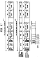
- FIG. 11(1) is an illustration showing a frame configuration of a hierarchical transmission system.
- One frame is configured by a frame-synchronizing-signal pattern comprising 32 BPSK-modulated symbols (20 latter-half symbols among 32 symbols are actually used as frame-synchronizing signal), a TMCC (Transmission and Multiplexing Configuration Control) pattern comprising 128 BPSK-modulated symbols to identify a multiple transmission configuration, a super-frame identifying signal pattern comprising 32 symbols (20 latter-half symbols among 32 symbols are actually used as super-frame identifying signal), a main signal of 203 8PSK(trellis-codec-8PSK)-modulated symbols, a burst symbol signal (BS) of four symbols in which a pseudo random noise (PN) signal is BPSK-modulated, a main signal of 202 8PSK(trellis-codec-8PSK)-modulated symbols, a burst symbol signal (BS) of four symbols in which a pseudo random noise (PN) signal is BPSK-modulated, ...,
- an intermediate-frequency signal of received signals received by a receiving circuit is demodulated by a demodulating circuit and two-series I and Q base-band signals (hereafter, I and Q base-band signals are also referred to as I and Q symbol-stream data) showing instantaneous values of I-axis and Q-axis orthogonal to each other for each symbol are obtained.
- I and Q base-band signals are also referred to as I and Q symbol-stream data
- Absolute phase generation to be fitted to a transmission-signal phase angle is performed by an absolute-phase generating circuit by acquiring a frame-synchronizing signal from the demodulated I and Q base-band signals, obtaining the present received-signal-phase rotation angle from a signal point arrangement of the acquired frame-synchronizing signal, and inversely rotating the phase of the demodulated I and Q base-band signals on the basis of the obtained received-signal phase rotation angle.
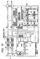
- an absolute-phase generating circuit of a receiver for receiving a wave to be PSK-modulated according to a conventional hierarchical transmission system is configured by a frame-sync detecting/regenerating circuit 2 serving as frame-synchronizing-signal acquiring means provided for the output side of a demodulating circuit 1 to acquire a frame-synchronizing signal, a remapper 7 serving as inversely-phase-rotating means comprising a ROM, and a received-signal-phase-rotation-angle detecting circuit 8 serving as received-signal-phase-rotation-angle detecting means.
- Symbol 9 denotes a transmission-configuration identifying circuit for identifying the multiple transmission configuration shown in FIG. 11(1), which outputs a two-bit modulation-system identifying signal DM.
- the demodulating circuit 1 orthogonally detects intermediate-frequency signals to obtain I and Q base-band signals.
- Symbols 60 and 61 denote multipliers for multiplying an intermediate-frequency signal IF by f c1 and f c2
- 62 and 63 denote A/D converters for A/D-converting outputs of the multipliers 60 and 61 at a sampling rate two times larger than a symbol rate
- 64 and 65 denote digital filters for applying band restriction to outputs of the A/D converters 62 and 63 through digital-signal processing
- 66 and 67 denote thinning circuits for thinning outputs of the digital filters 64 and 65 to 1/2 sampling rate and outputting two series of I and Q base-band signals (I and Q symbol-stream data) showing instantaneous values of I-axis and Q-axis for each symbol.
- the thinning circuits 66 and 67 transmit two series of I and Q base-band signals I(8) and Q(8) (a numeral in parentheses denotes the number of quantization bits which is hereafter also simply referred to as I and Q) respectively having 8 quantization bits (two's complement system).
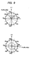
- FIG. 13(1) shows signal point arrangements on I-Q phase plane (also referred to as I-Q vector plane or I-Q signal space diagram) when using 8PSK for a modulation system.
- the 8PSK modulation system transmits a three-bit digital signal (abc) by one symbol. Combinations of bits constituting the symbol include such eight ways as (000), (001), (010), (011), (100), (101), (110), and (111). These three-bit digital signals are converted into signal point arrangements "0" to "7" on transmission-side I-Q phase plane in FIG. 12 (1) and this conversion is referred to as 8PSK mapping.
- bit string (000) is converted into signal point arrangement "0,” bit string (001) into signal point arrangement "1,” bit string (011) into signal point arrangement "2,” bit string (010) into signal point arrangement "3,” bit string (100) into signal paint arrangement "4,” bit string (101) into signal point arrangement "5,” bit string (111) into signal point arrangement "6,” and bit string (110) into signal point arrangement "7.”
- FIG. 13(2) shows signal point arrangements on I-Q phase plane at the time of using QPSK for a modulation system.
- the QPSK modulation system transmits two-bit digital signal (de) by one symbol. Combinations of bits constituting the symbol include such four ways as (00), (01), (10), and (11).
- bit string (00) is converted into signal point arrangement "1,” bit string (01) into signal point arrangement "3,” bit string (11) into signal point arrangement "5,” and bit string (10) into signal point arrangement "7.”
- FIG. 13(3) shows signal point arrangements at the time of using BPSK for a modulation system.
- the BPSK modulation system transmits one-bit digital signal (f) by one symbol.
- bit (0) is converted into signal point arrangement "0" and bit (1) into signal point arrangement "4.”
- the relation between signal point arrangement and arrangement number is the same for various modulation systems on the basis of 8BPSK.
- I-axis and Q-axis of QPSK and BPSK in a hierarchical transmission system coincide with I-axis and Q-axis of 8PSK.
- the reference carrier waves f c1 and f c2 can actually take various phase states for a carrier wave before modulated in inputs of the demodulating circuit 1, a received-signal point at the reception side has a phase position rotated by a certain angle ⁇ against the transmission side. Moreover, when a phase of a carrier wave before modulated in inputs of the demodulating circuit 1 fluctuates, e also fluctuates. When a phase of a received-signal point rotates against the transmission side at random, it is impossible to identify a received digital signal.
- ⁇ is equal to ⁇ /8
- a received-signal point of a digital signal (000) of a signal point arrangement "0" according to a transmission-side 8PSK modulation system is brought to the middle between signal point arrangements "0" and "1" at the reception side. Therefore, at the time of assuming that the digital signal (000) is received at the signal point arrangement "0,” it is judged that the signal is correctly received. However, at the time of assuming that the signal is received at the signal point arrangement "1,” it is erroneously judged that a digital signal (001) is received. Therefore, the carrier-wave regenerating circuit 10 corrects phases of the reference carrier waves f c1 and f c2 so that a received-signal point keeps a certain rotation angle against the transmission side and a digital signal is correctly identified.
- the reference carrier wave f c1 is generated by making a VCO (voltage control oscillator) 11 of the carrier-wave regenerating circuit 10 oscillate at a transmission-carrier-wave frequency and the reference carrier wave f c2 is generated by delaying a phase of an oscillation signal of the VCO 11 by 90° by a 90° phase shifter 12. Moreover, by changing a control voltage of the VCO 11, it is possible to change phases of the reference carrier waves f c1 and f c2 .
- VCO voltage control oscillator
- the carrier-wave regenerating circuit 10 is provided with phase error tables 13, 14-1 and 14-2, and 15-1 to 15-4 obtained by tabulating relations between various data sets of I and Q base-band signals I(8) and Q(8) and carrier-wave-phase-error data (hereafter also referred to as phase error data) ⁇ (8) of eight quantization bits (two's complement system) and respectively configured by a ROM for each of 8PSK, QPSK, and BPSK modulation systems (refer to FIG. 14).
- I and Q base-band signals I(8) and Q(8) are input to the phase error tables 13, 14-1 and 14-2, and 15-1 to 15-4 in parallel.
- a phase error table selectively enabled by a selector to be described later outputs phase error data ⁇ (8) corresponding to I and Q base-band signals I(8) and Q(8) input from the demodulating circuit 1.
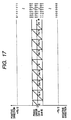
- the phase error table 13 is used for 8PSK, in which the relation between phase angle ⁇ (refer to FIG. 15) and phase error data ⁇ (8) of a received-signal point shown by I and Q base-band signals I(8) and Q(8) in symbols input from the demodulating circuit 1 on I-Q phase plane is constituted as shown in FIG. 17.
- a selector 16 enables (activates) only the phase error table 13 while the demodulating circuit 1 demodulates digital waves to be modulated according to the BPSK modulation system (designated by a modulation-system identifying signal DM output from a transmission-configuration identifying circuit 9 to be described later) in accordance with a clock CLK SYB (refer to FIG.
- the phase error data ⁇ (8) is converted into a phase error voltage by a D/A converter 17 and then, low-frequency components of the data are removed by an LPF 18 and the data is applied to the VCO 11 as a control voltage.
- the phase error data ⁇ (8) is equal to 0, outputs of the LPF 18 are not changed and therefore, phases of the reference carrier waves f c1 and f c2 are not changed.
- the phase error data ⁇ (8) is positive, an output of the LPF 18 is strengthened and phases of the reference carrier waves f c1 and f c2 are delayed.
- the phase error data ⁇ (8) is negative, an output of the LPF 18 is weakened and phases of the reference carrier waves f c1 and f c2 are advanced.
- phase error table 13 when a modulation system is 8PSK, the difference between a phase angle ⁇ of a received-signal point shown by I and Q base-band signals I(8) and Q(8) and a phase of the nearest one (which is a target phase convergent angle of the received-signal point) of signal point arrangements "0" to "7" is equal to phase error data ⁇ (8).
- phase error tables 14-1 and 14-2 are used for QPSK, in which the relation between phase angle ⁇ and phase error data ⁇ (8) of a received signal point shown by I and Q base-band signals I(8) and Q(8) in symbols on I-Q phase plane is constituted as shown in FIGS. 18 and 19.
- the selector 16 enables only the phase error table 14-1 when a received-signal-phase rotation angle ⁇ is equal to 0, 2 ⁇ /4, 4 ⁇ /4, or 6 ⁇ /4 while the demodulating circuit 1 demodulates digital waves to be modulated according to the QPSK modulation system in accordance with a clock CLK SYB at a symbol rate and reads phase error data ⁇ (8) corresponding to the set data of I and Q base-band signals I(8) and Q(8) out of the phase error table 14-1 whenever the demodulating circuit 1 outputs the I(8) and Q(8) for one symbol.
- the phase error table 14-1 is used when a modulation system uses QPSK and a received-signal-phase rotation angle ⁇ is equal to any one of 0, 2 ⁇ /4, 4 ⁇ /4, and 6 ⁇ /4, in which the difference between a phase angle ⁇ of a received-signal point shown by I and Q base-band signals I(8) and Q(8) and a phase of the nearest one (which is a target phase-convergent angle of the received-signal point) of signal point arrangements "1," "3,” “5,” and “7” is equal to phase error data ⁇ .
- the target phase convergent angle is equal to i ⁇ (2 ⁇ /4)+ ⁇ /4 .
- the selector 16 enables only the phase error table 14-2 when ⁇ is equal to ⁇ /4, 3 ⁇ /4, 5 ⁇ /4, or 7 ⁇ /4 while the demodulating circuit 10 demodulates digital waves to be modulated according to the QPSK modulation system and reads phase error data ⁇ (8) corresponding to the set data of I and Q base-band signals I(8) and Q(8) out of the phase error table 14-2 whenever the demodulating circuit 1 outputs the I(8) and Q(8) for one symbol.
- the phase error table 14-2 is used when a modulation system uses QPSK and a received-signal-phase rotation angle ⁇ is equal to any one of ⁇ /4, 3 ⁇ /4, 5 ⁇ /4, and 7 ⁇ /4, in which the difference between a phase angle ⁇ of a received-signal point shown by I and Q base-band signals I(8) and Q(8) and a phase of the nearest one (which is a target phase convergent angle of the received-signal point) of signal point arrangements "0,” "2,” “4,” and “6” is equal to phase error data ⁇ .
- the target phase convergent angle is equal to i ⁇ (2 ⁇ /4).
- phase error tables 15-1 to 15-4 are used for BPSK, in which the relation between phase angle ⁇ and phase error data ⁇ (8) of a received-signal point shown by I and Q base-band signals I(8) and Q(8) on I-Q phase plane is constituted as shown in FIGS. 21 to 24.
- the selector 16 enables only the phase error table 15-1 when a received-signal-phase rotation angle ⁇ due to phase correction of an 8PSK modulation portion is equal to 0 or 4 ⁇ /4 while the demodulating circuit 1 demodulates digital waves to be modulated according to the BPSK modulation system synchronously with a clock CLK SYB at a symbol rate and reads phase error data ⁇ (8) corresponding to the set data of I and Q base-band signals I(8) and Q(8) out of the phase error table 15-1 whenever the demodulating circuit 1 outputs the I(8) and Q(8) for one symbol.
- the phase error table 15-1 is used when a modulation system uses BPSK and a received-signal-phase rotation angle ⁇ is equal to either of 0 and 4 ⁇ /4, in which the difference between a phase angle ⁇ of a received-signal point shown by I and Q base-band signals I(8) and Q(8) and a phase of the nearest one (which is a target phase convergent angle of the received-signal point) of signal point arrangements "0" and "4" is equal to phase error data ⁇ .
- a phase angle ⁇ of a received-signal point shown by I and Q base-band signals I(8) and Q(8) and a phase of the nearest one (which is a target phase convergent angle of the received-signal point) of signal point arrangements "0" and "4" is equal to phase error data ⁇ .
- the target phase convergent angle is equal to i ⁇ (4 ⁇ /4).
- the selector 16 enables only the phase error table 15-2 when ⁇ is equal to ⁇ /4 or 5 ⁇ /4 while demodulating a digital wave to be modulated according to the BPSK modulation system and reads phase error data ⁇ (8) corresponding to I and Q base-band signals I(8) and Q(8) out of the phase error table 15-2 whenever the demodulating circuit 1 outputs the I(8) and Q(8) for one symbol.
- the phase error table 15-2 is used when a modulation system uses BPSK and a received-signal-phase rotation angle ⁇ is equal to either of ⁇ /4 and 5 ⁇ /4, in which the difference between a phase angle ⁇ of a received-signal point shown by I and Q base-band signals I(8) and Q(8) and a phase of the nearest one (which is a target phase convergent angle of the received-signal point) of signal point arrangements "1" and "5" is equal to phase error data ⁇ .
- a phase angle ⁇ of a received-signal point shown by I and Q base-band signals I(8) and Q(8) and a phase of the nearest one (which is a target phase convergent angle of the received-signal point) of signal point arrangements "1" and "5" is equal to phase error data ⁇ .
- the target phase convergent angle is equal to i ⁇ (4 ⁇ /4)+ ⁇ /4 .
- the selector 16 enables only the phase error table 15-3 when ⁇ is equal to 2 ⁇ /4 or 6 ⁇ /4 while demodulating a digital wave to be modulated according to the BPSK modulation system and reads phase error data ⁇ (8) corresponding to the set data of I and Q base-band signals I(8) and Q(8) out of the phase error table 15-3 whenever the demodulating circuit 1 outputs the I(8) and Q(8) for one symbol.
- the phase error table 15-3 is used when a modulation system uses BPSK and a received-signal-phase rotation angle ⁇ is equal to either of 2 ⁇ /4 and 6 ⁇ /4, in which the difference between a phase angle ⁇ of a received-signal point shown by I and Q base-band signals I(8) and Q(8) and a phase of the newest one (which is a target phase convergent angle of the received-signal point) of signal point arrangements "2" and "6" is equal to phase error data ⁇ .
- a phase angle ⁇ of a received-signal point shown by I and Q base-band signals I(8) and Q(8) and a phase of the newest one (which is a target phase convergent angle of the received-signal point) of signal point arrangements "2" and "6" is equal to phase error data ⁇ .
- the target phase convergent angle is equal to i ⁇ (4 ⁇ /4)+2 ⁇ /4 .
- the selector 16 enables only the phase error table 15-4 when ⁇ is equal to 3 ⁇ /4 or 7 ⁇ /4 while demodulating a digital wave to be modulated according to the BPSK modulation system and reads phase error data ⁇ (8) corresponding to the set data of I and Q base-band signals I(8) and Q(8) out of the phase error table 15-4 whenever the demodulating circuit 1 outputs the I(8) and Q(8) for one symbol.
- the phase error table 15-4 is used when a modulation system uses BPSK and a received-signal-phase rotation angle ⁇ is equal to either of 3 ⁇ /4 and 7 ⁇ /4, in which the difference between a phase angle ⁇ of a received-signal point shown by I and Q base-band signals I(8) and Q(8) and a phase of the nearest one (which is a target phase convergent angle of the received-signal point) of signal point arrangements "3" and "7" is equal to phase error data ⁇ .
- a phase angle ⁇ of a received-signal point shown by I and Q base-band signals I(8) and Q(8) and a phase of the nearest one (which is a target phase convergent angle of the received-signal point) of signal point arrangements "3" and "7" is equal to phase error data ⁇ .
- the target phase convergent angle is equal to i ⁇ (4 ⁇ /4)+3 ⁇ /4 .
- a frame-sync detecting/regenerating circuit 2 is configured by a BPSK demapper section 3, sync detecting circuits 40 to 47, a frame-synchronizing circuit 5, an OR gate circuit 53, and a frame-synchronizing-signal generator 6.
- a received-signal-phase-rotation-angle detecting circuit 8 is configured by delay circuits 81 and 82, a 0°/180° phase rotating circuit 83, averaging circuits 84 and 85, and a received-phase judging circuit 86.
- I and Q base-band signals I(8) and Q(8) output from the demodulating circuit 1 are input to the BPSK demapper section 3 of the frame-sync detecting/regenerating circuit 2 in order to acquire, for example, a BPSK-modulated frame-synchronizing signal and a BPSK-demapped bit stream B0 is output.
- the BPSK demapper section 3 is configured by, for example, a ROM.
- a frame-synchronizing signal In case of the hierarchical transmission system, a frame-synchronizing signal is transmitted by being BPSK-modulated so that a necessary C/N is minimized.
- a bit stream of a frame-synchronizing signal is also referred to as "SYNCPAT.”
- the bit stream is convened into a signal point arrangement "0" or "4" through the BPSK mapping shown in FIG. 13(3) at the transmission side and a converted symbol stream is transmitted.
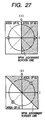
- FIG. 27(1) (0) is judged when a demodulated signal is received in a hatched area on reception-side I-Q phase plane and (1) is judged when the signal is received in a not-hatched area. That is, in FIG. 27(1), an output is classified into (0) or (1) depending on a judgement area in which the output is received out of two judgement areas divided by a BPSK judgement border line shown by a bold line in FIG. 27(1) and thereby, it is assumed that BPSK demapping is performed.
- I and Q base-band signals I(8) and Q(8) are input to the BPSK demapper section 3 for performing BPSK demapping and the bit stream B0 BPSK-demapped in the BPSK demapper section 3 is output.
- a demapper denotes a circuit for performing demapping.
- the bit stream B0 is input to the sync detecting circuit 40 in which a bit stream of a frame-synchronizing signal is acquired from the bit stream B0.
- the sync detecting circuit 40 has 20 D-flip-flops (hereafter referred to as D-F/Fs) D19 to D0 connected in series and a 20-stage shift register is constituted by these D-F/Fs D19 to D0.
- the bit stream B0 is input to the D-F/F D19 and successively shifted up to the D-F/F D0.
- predetermined logical inversion is applied to predetermined bits of outputs of the D-F/Fs D19 to D0 and then, the outputs are input to an AND gate 51.
- the output SYNA0 of the sync detecting circuit 40 is input to a frame-synchronizing circuit 5 through an OR gate circuit 53.
- an output SYNA of the OR gate circuit 53 repeatedly becomes a high potential every certain frame cycle, it is discriminated that a frame sync is established and a frame-synchronizing pulse is output every frame cycle.
- TMCC pattern in FIG. 11(1) header data showing their multiple configuration is multiplexed (TMCC pattern in FIG. 11(1)).
- the transmission-configuration identifying circuit 9 extracts TMCC showing a multiple configuration from a bit stream after a BPSK demapper input from the frame-synchronizing circuit 5 after it is discriminated that frame sync is established in the frame-sync detecting/regenerating circuit 2, decodes the TMCC, and outputs a modulation-system identifying signal DM showing to which modulation system the present I and Q base-band signals I and Q conform to the selector 16 and the like (refer to FIG. 11(2)).
- the received-signal-phase-rotation-angle detecting circuit 8 detects a received-signal-phase rotation angle ⁇ in accordance with a regenerated frame-synchronizing signal output from the frame-synchronizing-signal generator 6 after it is discriminated that frame sync is established in the frame-sync detecting/regenerating circuit 2 and outputs a three-bit received-signal-phase-rotation-angle signal AR(3) to the remapper 7 and the selector 16 of the carrier-wave regenerating circuit 10.
- the selector 16 of the carrier-wave regenerating circuit 10 After a modulation-system identifying signal DM is input from the transmission-configuration identifying circuit 9 and a received-signal-phase-rotation-angle signal AR(3) is input from the received-signal-phase-rotation-angle detecting circuit 8, the selector 16 of the carrier-wave regenerating circuit 10 reads phase error data ⁇ (8) out of a phase error table corresponding to a modulation system and a received-signal-phase rotation angle ⁇ and outputs the data ⁇ (8) to the D/A converter 17. However, before outputting the data, the selector 16 reads phase error data ⁇ (8) out of the phase error table 13 for 8PSK.
- the demodulating circuit 1 always operates as an 8PSK demodulating circuit before the transmission-configuration identifying circuit 9 identifies a multiple configuration and the received-signal-phase-rotation-angle detecting circuit 8 detects a received-signal-phase rotation angle ⁇ .
- a BPSK judgement border line shown by a bold line in FIG. 27(2) rotates by ⁇ /4 counterclockwise from the BPSK judgement border line shown by a bold line for BPSK demapping in FIG. 27(1) in the case of reception at the same phase as the transmission side.
- a BPSK demapper (refer to symbol 31 in FIG. 29) for performing the BPSK demapping shown in FIG.
- a bit stream BPSK-demapped by the BPSK demapper 31 serves as an output B1 of the BPSK demapper section 3 in FIG. 26.
- Bit streams BPSK-demapped by the BPSK demappers 32 to 37 serve as outputs B2 to B7 of the BPSK demapper section 3 in FIG. 26.
- a bit stream BPSK-demapped by the BPSK demapper 30 serves as an output B0 of the BPSK demapper section 3 in FIG. 26.
- Configurations of sync detecting circuits 41 to 47 are the same as the configuration of the sync detecting circuit 40.
- a frame-synchronizing signal is acquired by one of the sync detecting circuits 40 to 47 independently of phase rotation of a base-band signal according to a phase state of the reference carrier wave f c1 or f c2 regenerated by the carrier-wave regenerating circuit 10 of the demodulating circuit 1 and a high-potential SYNAn (n is one of integers 0 to 7) is transmitted from the sync detecting circuit acquiring the frame-synchronizing signal.
- the SYNAn output from one of the sync detecting circuits 40 to 47 is input to the OR gate circuit 53 and a logical sum SYNA of the SYNAn is output from the OR gate circuit 53.
- the frame-synchronizing circuit 5 judges that frame sync is established when it is confirmed that a high potential of SYNA is alternately repeatedly input every certain frame interval and outputs a frame-synchronizing pulse FSYNC every frame cycle.
- the frame-synchronizing-signal generator 6 generates a bit stream same as a pattern SYNCPAT of a frame-synchronizing signal acquired by the BPSK demapper 3, sync detecting circuits 40 to 47, and frame-synchronizing circuit 5 (the bit stream is referred to as a regenerated frame-synchronizing signal) in accordance with the frame-synchronizing pulse FSYNC output by the frame-synchronizing circuit 5.
- the transmission-configuration identifying circuit 9 inputs bit streams B0 to B7 output by the BPSK demapper 3 of the frame-sync detecting/regenerating circuit 2, SYNA0 to SYNA7 output by sync detecting circuits 40 to 47, and a frame-synchronizing pulse FSYNC output by the frame-synchronizing circuit 5. Moreover, when the circuit 9 inputs the frame-synchronizing pulse FSYNC, It captures a bit stream Bn of a system repeatedly becoming a high potential in SYNA0 to SYNA7, extracts and decodes the TMCC pattern in FIG.
- absolute phase generation is described below which is realized by obtaining the present received-signal-phase rotation angle from a signal point arrangement of an acquired frame-synchronizing signal and inversely rotating the phase of demodulated I and Q base-band signals I(8) and Q(8) in accordance with the obtained received-signal-phase rotation angle.
- Each symbol of a symbol stream of a frame-synchronizing signal which is BPSK-mapped at the transmission side, transmitted, and demodulated to I and Q base-band signals I(8) and Q(8) by the demodulating circuit 1 is demapped to bit (0) or (1) by the BPSK demapper section 3 and the difference between phases of a symbol demapped to bit (0) and a symbol demapped to bit (1) is equal to 180°. Therefore, by rotating the phase of the symbol demapped to bit (1) at the frame-synchronizing-signal portion of a received symbol stream by 180°, symbol streams which are all demapped to bit (0) are obtained.
- the frame-synchronizing-signal generator 6 by receiving a frame-synchronizing pulse output from the frame-synchronizing circuit 5, the frame-synchronizing-signal generator 6 generates a bit stream same as the pattern SYNCPAT of an acquired frame-synchronizing signal and supplies the bit stream to the 0°/180° phase-rotating circuit 83 of the received-signal-phase-rotation-angle detecting circuit 8 as a regenerated frame-synchronizing signal.
- the 0°/180° phase-rotating circuit 83 rotates the phase of I and Q base-band signals by 180° for bit (1) of a bit stream of a supplied regenerated frame-synchronizing signal but the circuit 83 does not rotate the phase of I and Q base-band signals for bit (0) of the bit stream in accordance with a bit (0) or (1) of a bit stream of a supplied regenerated frame-synchronizing signal.
- the timing of a bit stream of a regenerated frame-synchronizing signal transmitted from the frame-synchronizing-signal generator 6 is made to coincide with the timing of a symbol stream of a frame-synchronizing signal in I and Q symbol streams by the delay circuits 81 and 82 at the input side of the 0°/180° phase-rotating circuit 83.
- the delay circuits 81 and 82 respectively open their output gate only while a frame-synchronizing-signal-interval signal is output from the frame-synchronizing-signal generator 6. Therefore, I and Q symbol streams DI(8) and DQ(8) of a frame-synchronizing-signal portion are output from the delay circuits 81 and 82.
- a symbol portion corresponding to bit (1) of a bit stream of a regenerated frame-synchronizing signal is phase-rotated by 180° by the 0°/180° phase-rotating circuit 83 but a symbol portion corresponding to bit (0) is transmitted to the averaging circuits 84 and 85 as symbol streams VI(8) and VQ(8) without being phase-rotated. Because all of 20 bits of the symbol streams VI(8) and VQ(8) constituting a frame-synchronizing signal are equal to bit (0), the symbol streams VI(8) and VQ(8) serve as symbol streams when receiving a signal BPSK-mapped at the transmission side.
- FIG. 30(2) shows the signal point arrangement of I and Q symbol streams VI(8) and VQ(8) after converted by the 0°/180° phase-rotating circuit 83.
- I and Q symbol streams VI(8) and VQ(8) are averaged in order to stably obtain a signal point arrangement even if a slight phase change or amplitude fluctuation occurs in a received base-band signal due to deterioration of a received C/N occurs.
- a received-signal point [AVI(8), AVQ(8)] of a signal obtained by BPSK-mapping bit (0) by the averaging circuits 84 and 85 is obtained.
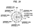
- the received-signal point [AVI(8), AVQ(8)] is input to the received-phase judging circuit 86 comprising a ROM and a received-signal-phase rotation angle ⁇ is obtained in accordance with a received-signal-phase-rotation-angle judging table on the AVI-AVQ phase plane shown in FIG. 31 and a phase-rotation-angle signal AR(3) of three bits (natural binary number) corresponding to the ⁇ is output.
- the remapper 7 comprising a ROM receives the received-signal-phase-rotation-angle signal AR(3) to rotate the phase of I and Q base-band signals I(8) and Q(8) in accordance with the received-signal-phase-rotation-angle signal AR(3), an absolute phase is generated.
- the remapper 7 constitutes a phase converting circuit for making the signal point arrangement of received I and Q base-band signals I(8) and Q(8) same as that of the transmission side.
- a received-signal-phase rotation angle ⁇ is calculated by the received-signal-phase-rotation-angle detecting circuit 8 and a received-signal-phase-rotation-angle signal AR(3) corresponding to the received-signal-phase rotation angle ⁇ is supplied to the remapper 7.
- the decimal notation R of the received-signal-phase-rotation-angle signal AR(3) is one of integers 0 to 7 and the relation with the received-signal-phase rotation angle ⁇ is defined as shown by the following expression (1).
- R ⁇ /( ⁇ /4)
- ⁇ is equal to m ⁇ ( ⁇ /4) and m is one of integers 0 to 7.
- I' Icos( ⁇ ) - Qsin( ⁇ )
- Q' Isin( ⁇ ) - Qcos( ⁇ )
- the transmission-configuration identifying circuit 9 previously identifies a transmission configuration and then the received-signal-phase-rotation-angle detecting circuit 8 detects a received-signal-phase rotation angle or the received-signal-phase-rotation-angle detecting circuit 8 previously detects the received-signal-phase rotation angle and then the transmission-configuration identifying circuit 9 identifies the transmission configuration. Moreover, it is possible to simultaneously perform the detection of a received-signal-phase rotation angle by the received-signal-phase-rotation-angle detecting circuit 8 and the identification of a transmission configuration by the transmission-configuration identifying circuit 9.
- phase error table 13 for correcting the phase of the reference carrier waves f c1 and f c2 for demodulation according to the 8PSK modulation system
- phase error tables 14-1 and 14-2 for correcting the phase of the reference carrier waves f c1 and f c2 for demodulation according to the QPSK modulation system
- phase error tables 15-1 to 15-4 for correcting the phase of the reference carrier waves f c1 and f c2 for demodulation according to the BPSK modulation system. Therefore, there is a problem that a necessary memory capacity increases.
- a receiver of the present invention comprises demodulating means for demodulating a signal to be PSK-modulated in which digital signals modulated by 2-phase, 4-phase, and 8-phase PSK modulation systems are time-multiplexed by using a carrier wave regenerated by carrier-wave regenerating means and outputting I and Q symbol-stream data in symbols; received-signal-phase-rotation-angle detecting means for detecting a phase rotation angle ⁇ of I and Q symbol-stream data against the transmission side for each symbol output from the demodulating means, inversely-phase-rotating means for rotating the phase of I and Q symbol-stream data for each symbol output from the demodulating means by - ⁇ against the phase rotation angle ⁇ detected by the received-signal-phase-rotation-angle detecting means, generating the absolute phase of the phase of the I and Q symbol-stream data, and outputting the absolute phase; and modulation-system identifying means for identifying a modulation system currently demodulated by the demodulating means; wherein the inversely-phase-rotating
- Inversely-phase-rotating means outputs I and Q symbol-stream data absolute-phase-generated by phase-rotating I and Q symbol-stream data for each symbol output from demodulating means by - ⁇ and moreover, outputs I and Q symbol-stream data phase-rotated by ⁇ ( ⁇ + ⁇ ') through time sharing when assuming a shift angle up to a target phase convergent point of a received-signal point shown by an absolute-phase-generated I and Q symbol-stream data set viewed in the positive or negative direction of I-axis included in a phase error table in accordance with a modulation system identified by modulation-system identifying means as ⁇ '.
- Phase-error detecting means reads phase error data out of a phase error table by using the I and Q symbol-stream data set.
- phase error data is data corresponding to a modulation system of a received signal currently demodulated by demodulating means, a received-signal-phase rotation angle against the transmission side, and a received-signal point, carrier-wave regenerating means requires only one phase error table. Therefore, it is possible to decrease the number of phase error tables to be provided for carrier-wave regenerating means and greatly simplify a circuit configuration.
- FIG. 1 An embodiment of the present invention will be described below by referring to FIG. 1.
- FIG. 1 is a block diagram of an essential portion of a broadcast receiver (wave-to-be-PSK-modulated receiver) of the present invention, in which a component same as that in FIG. 12 is provided with the same symbol.
- the carrier-wave regenerating circuit has seven phase error tables 13, 14-1 and 14-2, and 15-1 to 15-4 and reads phase error data corresponding to a set of I and Q symbol-stream data I(8) and Q(8) output from the demodulating circuit.
- the carrier-wave regenerating circuit has only the phase error table 15-1A and reads phase error data corresponding to an I and Q symbol-stream data set absolute-phase-generated by a remapper 7A.
- the remapper 7A captures ⁇ I t (8), Q t (8) ⁇ at the inactivation timing of the CLK SYB to output an I and Q symbol-stream data set ⁇ RI 0t (8), RQ 0t (8) ⁇ phase-rotated by - ⁇ and captures ⁇ I t (8), Q t (8) ⁇ at the activation timing of the CLK SYB to output an I and Q symbol-stream data set ⁇ RI 1t (8), RQ 1t (8) ⁇ phase-rotated by -( ⁇ + ⁇ ').
- the phase error table 15-1A provided for a carrier-wave regenerating circuit 10A is obtained by forming relations between various data sets of I and Q symbol-stream data RI(8) and RQ(8) (a range of RI(8) ⁇ 0) absolute-phase-generated by the remapper 7A in accordance with the BPSK modulation system and 8 quantization bits (also referred to as phase error data of two's complement system) ⁇ (8) into a ROM table, which is formed by using a range in which I coordinate on I-Q phase plane of I and Q symbol-stream data RI(8) and RQ(8) is equal to or more than 0 (refer to FIG.
- received-signal points 8PSK-mapped to signal point arrangements "0" to "7" at the transmission side are respectively kept in any one of areas KR 0 to KR 7 eight-divided about phases 0, ⁇ /4, 2 ⁇ /4, 3 ⁇ /4, 4 ⁇ /4, 5 ⁇ /4, 6 ⁇ /4, and 7 ⁇ /4 on the I-Q phase plane in FIG. 4.
- a target phase convergent angle of the received-signal point P k according to the phase correcting operation for the reference carrier waves f c1 and f c2 by the carrier-wave regenerating circuit 10A is equal to i ⁇ ( ⁇ /4).
- a shift angle ⁇ ' in the positive direction of I-axis becomes equal to i ⁇ ( ⁇ /4).
- phase error data ⁇ (8) is obtained which corresponds to RI 0k (8) and RQ 0k (8) when moving the solid line graph in FIG. 3 by 2 ⁇ /4 in the positive direction of ⁇ -axis and replacing it with a broken-line graph.
- phase error data corresponding to absolute-phase-generated I and Q symbol-stream data I 0k (8) and Q 0k (8) in the phase error table in FIG. 17 is obtained by ⁇ 1k (8). Because the I and Q symbol-stream data I 0k (8) and Q 0k (8) are absolute-phase-generated, a target phase convergent angle of a received-signal point P k becomes same as a signal point arrangement of the transmission side and thus, a carrier-wave phase error to the received-signal point P k according to the 8PSK modulation system is correctly obtained independently of a received-signal-phase rotation angle ⁇ .
- a target phase convergent angle of the received-signal point P k according to the phase correcting operation to the reference carrier waves f c1 and f c2 by the carrier-wave regenerating circuit 10A is equal to i ⁇ (2 ⁇ /4)+ ⁇ /4 .
- a shift angle ⁇ ' in the positive direction of I-axis becomes i ⁇ (2 ⁇ /4)+ ⁇ /4 .
- phase error data ⁇ (8) is obtained which corresponds to RI 0k (8) and RQ 0k (8) when moving the solid table in FIG. 3 by ⁇ /4 in the positive direction of ⁇ -axis and replacing the table with the graph in FIG. 5.
- phase error data corresponding to absolute-phase-generated I and Q symbol-stream data I 0k (8) and Q 0k (8) in the phase error table in FIG. 18 is obtained by ⁇ 1k (8). Because the I and Q symbol-stream data I 0k (8) and Q 0k (8) are absolute-phase-generated, a target phase convergent angle of the received-signal point P k becomes the same as a transmission-side signal point arrangement and a carrier-wave phase error to the received-signal point P k according to the QPSK modulation system is correctly obtained independently of a received-signal-phase rotation angle ⁇ .
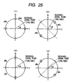
- received-signal points BPSK-mapped to signal point arrangements "0" and "4" at the transmission side are respectively kept in either of areas GR 0 and GR 1 two-divided about phases 0 and 4 ⁇ /4 on the I-Q phase plane in FIG. 25(1).
- a target phase convergent angle of the received-signal point P k according to the phase correcting operation to the reference carrier waves f c1 and f c2 by the carrier-wave regenerating circuit 10A is equal to i ⁇ (4 ⁇ /4).
- a shift angle ⁇ ' in the positive direction of I-axis becomes i ⁇ (4 ⁇ /4) (however, when measuring the shift angle ⁇ ' in the negative direction of I-axis, the ⁇ ' becomes i ⁇ (4 ⁇ /4)- ⁇ ) .
- phase error data ⁇ (8) is obtained which corresponds to RI 0k (8) and RQ 0k (8) when moving the solid line graph in FIG. 3 by ⁇ in the positive direction of ⁇ -axis and replacing the graph with the graph in FIG. 6.
- phase error data corresponding to absolute-phase-generated I and Q symbol-stream data I 0k (8) and Q 0k (8) in the phase error table in FIG. 21 is obtained by ⁇ 1k (8). Because the I and Q symbol-stream data I 0k (8) and Q 0k (8) are absolute-phase-generated, a target phase convergent angle of the received-signal point P k becomes the same as a transmission-side signal point arrangement and a carrier-wave phase error to the received-signal point P k according to the BPSK modulation system is correctly obtained independently of a received-signal-phase rotation angle ⁇ .
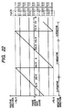
- FIG. 7 is a block diagram showing a specific configuration of the phase-error detecting circuit 70 and FIG. 8 is a time chart showing operations of the phase-error detecting circuit 70.
- the configuration of the phase-error detecting circuit 70 is described below by referring to FIG. 8.
- An angle ⁇ ' takes any one of 0, ⁇ /4, 2 ⁇ /4, 3 ⁇ /4, 4 ⁇ /4, 5 ⁇ /4, 6 ⁇ /4, and 7 ⁇ /4 which are respectively shown by one of two-bit three-digit values such as (000), (001), (010), (011), (100), (101), (110), and (111) in order.
- the former is latched by the latch circuits 68 and 69 and output to the rear stage.
- the selector 73 selects (000) because P k is kept in the area GR 0 in FIG. 25(1) and the target phase convergent angle is equal to 0 when RI 0k (8) is equal to or larger than 0 and selects (100) because P k is kept in the area GR 1 in FIG. 25(1) and the target phase convergent angle is equal to 4 ⁇ /4 when RI 0k (8) is smaller than 0.
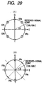
- the selector 74 selects (001) because P k is kept in the area ER 0 in FIG. 20(1) and a target phase convergent angle is equal to ⁇ /4 when RI 0k (8) is equal to or larger than 0 and RQ 0k (8) is equal to or larger than 0 and selects (011) because P k is kept in the area ER 1 in FIG. 20(1) and a target phase convergent angle is equal to 3 ⁇ /4 when RI 0k (8) is smaller than 0 and RQ 0k (8) is equal to or larger than 0.
- the selector 74 selects (101) because P k is kept in the area ER 2 in FIG.
- a target phase convergent angle is equal to 5 ⁇ /4 when RI 0k (8) is smaller than 0 and RQ 0k (8) is smaller than 0 and selects (111) because P k is kept in the area ER 3 in FIG. 20(1) and a target phase convergent angle is equal to 7 ⁇ /4 when RI 0k (8) is smaller than 0 and RQ 0k (8) is equal to or larger than 0.
- a phase angle of a received-signal point shown by -RI 0k (8) and -RQ 0k (8) is equal to a value obtained by adding ⁇ to a phase angle ⁇ of a received-signal point shown by original RI 0k (8) and RQ 0k (8).
- the selector 76 directly inputs RI(8) and RQ(8) output from the remapper 7A to the phase error table 15-1A while CLK SYB is activated and makes the table 15-1A output phase error data ⁇ (8) corresponding to the RI(8) and RQ(8) to read the data ⁇ (8).
- a selector 79 is connected to the other input side of the adder 78 to output (0101) when RI 0k (1) shows RI 0k (8) ⁇ 0 and outputs (1101) correspondingly to the fact that ⁇ is added to a phase angle ⁇ of a received-signal point shown by RI 0k (8) and RQ 0k (8) when code inversion is performed by the inverting circuit 75 when the RI 0k (1) shows RI 0k (8) ⁇ 0. Then, the adder 78 performs four-bit addition of two inputs.
- the demodulated portion shows a shift angle ⁇ ' up to a target phase convergent angle of a received-signal point P k shown by RI 0k (1) and RQ 0k (1) viewed in the positive direction of I-axis. Therefore, the adder 78 outputs the shift angle ⁇ ' as BR SPSK (3).
- Symbol 80 denotes a selector which outputs an input supplied from the selector 73 as BR(3) showing a shift angle ⁇ ' while the demodulating circuit 1A demodulates the BPSK-modulated portion, outputs an input supplied from the selector 74 as the BR(3) showing the shift angle ⁇ ' while the demodulating circuit 1A demodulates the QPSK-modulated portion, and outputs an input supplied from the selector 78 as the BR(3) showing the shift angle ⁇ ' while the demodulating circuit 1A demodulates the QPSK-modulated portion in accordance with a modulation-system identifying signal DM input from the transmission-configuration identifying circuit 9.
- the BR(3) shows a shift angle ⁇ ' up to a target phase convergent angle according to a modulation system currently demodulated by the demodulating circuit 1A of a received-signal point P k shown by the set data of absolute-phase-generated I and Q symbol-stream data RI 0k (8) and RQ 0k (8) viewed in the positive direction of I-axis while CLK SYB is inactivated and in the period after the timing signal T2.
- Symbol 81 denotes a three-bit adder (however, carry to fourth bit is not performed) which adds a received-signal-phase-rotation-angle detecting signal AR(3) output by the received-signal-phase-rotation-angle detecting circuit 8 to an output of the selector 80.
- Symbol 82 denotes a latch circuit which latches an output of the adder 81 in accordance with a timing signal T3 input while CLK SYB is inactivated and in the period after the timing signal T2 and outputs CR(3) showing ( ⁇ + ⁇ ') to the remapper 7A.
- the remapper 7A outputs RI 1k (8) and RQ 1k (8) whose phases are rotated by -( ⁇ + ⁇ ') against I k (8) and Q k (8).
- Other components are completely the same as those in FIG. 12.
- the BP 8PSK (3) shows a shift angle ⁇ ' up to a target phase convergent angle of a received-signal point P 0t shown by RI 0t (1) and RQ 0t (1) viewed in the positive direction of I-axis when regarding that every received signal follows the 8PSK modulation system (refer to FIG. 9(1)). Therefore, a received-signal point P 1t according to RI 1t (1) and RQ 1t (1) phase-rotated by the remapper 7A by ⁇ ( ⁇ + ⁇ ') shown by CR(3) is kept in a range of ⁇ /4 about a phase 0 on I-Q phase plane as shown in FIG. 9(2).
- the data ⁇ 1t (8) is converted into a phase error voltage by the D/A converter 17 and then, low-frequency components are extracted from the voltage by the LPF 18, and the voltage is applied to the VCO 11 as a control voltage.
- the phase error data ⁇ 1t (8) is equal to 0, outputs of the LPF 18 are not changed or phases of the reference carrier waves f c1 and f c2 are not changed.
- phase error data ⁇ (8) is positive, outputs of the LPF 18 are strengthened and the phase of the reference carrier waves f c1 and f c2 is delayed.
- the phase error data ⁇ (8) is negative, outputs of the LPF 18 are weakened and the phase of the reference earner waves f c1 and f c2 is advanced.
- the frame-sync detecting/regenerating circuit 5 acquires a frame-synchronizing signal in accordance with I t (8) and Q t (8) and outputs a frame-synchronizing pulse, regenerated frame-synchronizing signal, and frame-synchronizing-signal-interval signal.
- the transmission-configuration identifying circuit 9 When receiving a frame-synchronizing pulse FSYNC, the transmission-configuration identifying circuit 9 captures a bit stream Bn of a system repeatedly becoming a high potential among SYNA0 to SYNA7, extracts the TMCC pattern in FIG. 11(1) by using a predetermined timing signal generated from a frame-synchronizing pulse FSYNC and decodes the pattern, and outputs a modulation-system identifying signal DM showing which modulation system the present I t (8) and Q t (8) depend on (refer to FIG. 11(2)).
- the remapper 7A when assuming that the received-signal-phase rotation angle ⁇ w is previously detected, the remapper 7A outputs absolute-phase-generated I 0t (8) and Q 0t (8) obtained by inversely phase-rotating I t (8) and Q t (8) by - ⁇ w . Because CR(3) output by the phase-error detecting circuit 70 is equal to ( ⁇ w + ⁇ '), a received-signal point P 1t according to RI 1t (1) and RQ 1t (1) shown by CR(3) phase-rotated by -( ⁇ w + ⁇ ') by the remapper 7A is kept in a range of ⁇ /4 about a phase 0 on I-Q phase plane as shown in FIG.
- the transmission-configuration identifying circuit 9 identifies a multiple configuration and outputs a modulation-system identifying signal DM showing in which modulation-system portion the present I and Q symbol streams I t (8) and Q t (8) output from the demodulating circuit 1A are included after operations of the received-signal-phase-rotation-angle detecting circuit 8, the selector 80 of the phase-error detecting circuit 70 selects and outputs an output of the adder 78 when the DM shows 8PSK.
- a received-signal point P 0t according to outputs I 0t (8) and Q 0t (8) of the remapper 7A is kept in a range of ⁇ /4 about the phase 3 ⁇ /4 of the signal point arrangement "3" due to absolute phase generation similarly to the case of the transmission side.
- the phase-error detecting circuit 70 is able to output phase error data for converging received-signal points viewed through RI 0t (8) and RQ 0t (8) into a phase 3 ⁇ /4 to a D/A converter 18 by reading phase error data ⁇ 1t (8) corresponding to RI 1t (8) and RQ 1t (8) out of the phase error table 15-1A and latching the data ⁇ 1t (8).
- the circuit 70 is able to output phase error data for converging received-signal points viewed through outputs RI 0t (8) and RQ 0t (8) of the remapper 7A into phases 0, ⁇ /4, 2 ⁇ /4, 4 ⁇ /4, 5 ⁇ /4, 6 ⁇ /4, and 7 ⁇ /4 to the D/A converter 18 in the completely same manner as the above described.
- the selector 80 of the phase-error detecting circuit 70 selects and outputs an output of the selector 74 when DM shows QPSK.
- a received-signal point of a digital signal (de) QPSK-mapped to a transmission-side signal point arrangement "7" is kept in a range of 2 ⁇ /4 about a phase 2 ⁇ /4 of a signal point arrangement "2" when viewed through I t (8) and Q t (8) which are outputs of the demodulating circuit 1A.
- a received-signal point P 0t according to outputs I 0t (8) and Q 0t (8) of the remapper 7A is kept in a range of 2 ⁇ /4 about a phase 7 ⁇ /4 of the signal point arrangement "7" due to absolute phase generation similarly to the case of the transmission side.
- the phase-error detecting circuit 70 is able to output phase error data for converging a received-signal point viewed through RI 0t (8) and RQ 0t (8) into a phase 7 ⁇ /4 to the D/A converter 18 by reading phase error data ⁇ 1t (8) corresponding to RI 1t (8) and RQ 1t (8) out of the phase error table 15-1A and latching the data ⁇ 1t (8).
- the circuit 70 is able to output phase error data for converging received-signal points viewed through outputs RI 0t (8) and RQ 0t (8) of the remapper 7A into phases ⁇ /4, 3 ⁇ /4, and 5 ⁇ /4 to the D/A converter 18 in the completely same manner as the above.
- the selector 80 of the phase-error detecting circuit 70 selects and outputs an output of the selector 74 when DM shows QPSK.
- a received-signal point of a digital signal (f) BPSK-mapped to a transmission-side signal point arrangement "1" is kept in a range of 4 ⁇ /4 about a phase 7 ⁇ /4 of a signal point arrangement "7” when viewed through I t (8) and Q t (8) which are outputs of the demodulating circuit 1A.
- a received-signal point P 0t according to outputs I 0t (8) and Q 0t (8) of the remapper 7A is kept in a range of 4 ⁇ /4 about a phase 4 ⁇ /4 of the signal point arrangement "1" due to absolute phase generation similarly to the case of the transmission side.
- the phase-error detecting circuit 70 is able to output phase error data for converging a received-signal point viewed through RI 0t (8) and RQ 0t (8) into a phase 4 ⁇ /4 to the D/A converter 18 by reading phase error data ⁇ 1t (8) corresponding to RI 1t (8) and RQ 1t (8) out of the phase error table 15-1A and latching the data ⁇ 1t (8).
- the circuit 70 is able to output phase error data for converging received-signal points viewed through outputs RI 0t (8) and RQ 0t (8) of the remapper 7A into a phase 0 to the D/A converter 18 in the completely same manner as the above.
- the received-signal-phase-rotation-angle detecting circuit 8 repeatedly detects a received-signal-phase rotation angle. Also when ⁇ w has a value other than 3 ⁇ /4, the phase-error detecting circuit 70 completely similarly operates. Therefore, the circuit 70 is able to output phase error data for converging a received-signal point viewed from the output side of the remapper 1A into a phase same as that of the transmission side to the D/A converter 18 independently of a modulation system or a value ⁇ w of an original digital signal.
- the remapper 7A outputs I and Q symbol-stream data I 0t and Q 0t absolute-phase-generated by inversely phase-rotating I and Q symbol-stream data I t and Q t for each symbol output from the demodulating circuit 1A by - ⁇ and moreover, outputs I and Q symbol-stream data I 1t and Q 1t inversely phase-rotated by ⁇ ( ⁇ + ⁇ ') by assuming a shift angle up to a target phase convergent angle of a received-signal point shown by an absolute-phase-generated I and Q symbol-stream data set viewed in the positive direction or negative direction of I-axis included in a phase error table for each modulation system through time sharing as ⁇ '.
- the phase-error detecting circuit 70 reads phase error data ⁇ 1t (8) out of the phase error table 15-1A.
- the phase error data ⁇ 1t (8) serves as data corresponding to a modulation system of a received signal currently demodulated by the demodulating circuit 1A, a received-signal-phase rotation angle ⁇ against the transmission side viewed from an output point of the demodulating circuit 1A, and a phase angle ⁇ of a received-signal point. Therefore, it is enough to provide only one phase error table for the carrier-wave regenerating circuit 10A and thus, it is possible to decrease the number of phase error tables to be provided for the carrier-wave regenerating circuit 10A and greatly simplify a circuit configuration.
- a table using an area of I ⁇ 0 of I-Q phase plane as a domain is provided for the phase error table 15-1A.
- BR(3) output by the selector 80 of the phase-error detecting circuit 70 is set so as to show a shift angle ⁇ ' up to a target phase convergent angle of a received-signal point shown by I and Q symbol-stream data for each symbol after absolute-phase-generated by the remapper 7A viewed in the negative direction of I-axis according to a modulation system currently demodulated by a demodulating circuit.
- the selector 73 in FIG. 7 so as to output (100) when an output Ri(1) of the latch circuit 71 shows an output RI(8)>0 of the remapper 7A and output (000) when the output Ri(1) shows RI(8) ⁇ 0; set the selector 74 so as to select and output (001) for RI(8) ⁇ 0 and RQ(8) ⁇ 0, (011) for RI(8) ⁇ 0 and RQ(8) ⁇ 0, (101) for RI(8) ⁇ 0 and RQ(8) ⁇ 0, (111) for RI(8) ⁇ 0 and RQ(8) ⁇ 0 in accordance with the combination of positive and negative of RI(8) and RQ(8) shown by the outputs Ri(1) and Rq(1) of the latch circuits 71 and 72; and set the selector 76 so as to directly input the outputs RI(8) and RQ(8) of the remapper 7A to the phase error table 15-1A when Ri(1) shows RI(8) ⁇ 0 and input -RI(8) and -RQ(8) serving as the outputs of the inverting circuit 75 to the
- the BR(3) output by the selector 80 of the phase-error detecting circuit 70 so as to show a shift angle ⁇ ' up to a target phase convergent angle of a received-signal point shown by I and Q symbol-stream data for each symbol after absolute-phase-generated by the remapper 7A viewed in either of the positive direction and negative direction of I-axis according to a modulation system currently demodulated by a demodulating circuit.
- the present invention it is enough to provide only one phase error table for carrier-wave regenerating means and thereby, it is possible to decrease the number of phase error tables to be provided for the carrier-wave regenerating means and greatly simplify a circuit configuration.
Landscapes
- Engineering & Computer Science (AREA)
- Computer Networks & Wireless Communication (AREA)
- Signal Processing (AREA)
- Digital Transmission Methods That Use Modulated Carrier Waves (AREA)
Applications Claiming Priority (3)
| Application Number | Priority Date | Filing Date | Title |
|---|---|---|---|
| JP3373298 | 1998-01-29 | ||
| JP3373298 | 1998-01-29 | ||
| PCT/JP1999/000249 WO1999039485A1 (fr) | 1998-01-29 | 1999-01-22 | Recepteur |
Publications (3)
| Publication Number | Publication Date |
|---|---|
| EP1052818A1 true EP1052818A1 (fr) | 2000-11-15 |
| EP1052818A4 EP1052818A4 (fr) | 2005-07-20 |
| EP1052818B1 EP1052818B1 (fr) | 2008-03-19 |
Family
ID=12394589
Family Applications (1)
| Application Number | Title | Priority Date | Filing Date |
|---|---|---|---|
| EP99901146A Expired - Lifetime EP1052818B1 (fr) | 1998-01-29 | 1999-01-22 | Récepteur |
Country Status (6)
| Country | Link |
|---|---|
| US (1) | US6717993B1 (fr) |
| EP (1) | EP1052818B1 (fr) |
| CN (1) | CN1155208C (fr) |
| CA (1) | CA2318988C (fr) |
| DE (2) | DE69938388T2 (fr) |
| WO (1) | WO1999039485A1 (fr) |
Families Citing this family (8)
| Publication number | Priority date | Publication date | Assignee | Title |
|---|---|---|---|---|
| JP3773093B2 (ja) * | 2000-05-11 | 2006-05-10 | 富士通株式会社 | ディジタル信号検出器、ディジタル復調器、ディジタル信号の検出方法、およびディジタル復調器の同期検波方法 |
| JP2002141962A (ja) * | 2000-11-01 | 2002-05-17 | Mitsubishi Electric Corp | キャリア再生回路およびロック検出回路 |
| JP4484355B2 (ja) * | 2000-11-22 | 2010-06-16 | 富士通マイクロエレクトロニクス株式会社 | 復調装置、放送システム及び放送受信装置 |
| US7680260B2 (en) * | 2005-05-03 | 2010-03-16 | Avaya Inc. | Detecting a voice mail system answering a call |
| JP2007074618A (ja) * | 2005-09-09 | 2007-03-22 | Sony Corp | 無線通信装置及び無線通信方法、並びにコンピュータ・プログラム |
| KR100785767B1 (ko) * | 2005-11-11 | 2007-12-18 | 한국전자통신연구원 | 구적오차가 있는 m-psk 시스템의 심볼오율 성능 개선장치 및 방법 |
| JP2007142881A (ja) * | 2005-11-18 | 2007-06-07 | Fujitsu Ltd | 通信システム及び通信方法並びに送信機及び受信機 |
| US8526454B2 (en) * | 2009-03-27 | 2013-09-03 | Nokia Corporation | Apparatus and method for bit remapping in a relay enhanced communication system |
Family Cites Families (5)
| Publication number | Priority date | Publication date | Assignee | Title |
|---|---|---|---|---|
| US4641323A (en) * | 1983-02-07 | 1987-02-03 | Tsang Chung K | Multi-phase PSK demodulator |
| JP2513331B2 (ja) * | 1989-11-10 | 1996-07-03 | 日本電気株式会社 | 搬送波再生器 |
| JP3391015B2 (ja) * | 1994-07-20 | 2003-03-31 | 日本電信電話株式会社 | ディジタル処理直交変調器 |
| JP3145003B2 (ja) * | 1995-03-23 | 2001-03-12 | 株式会社東芝 | 直交周波数分割多重伝送方式とその送信装置および受信装置 |
| JP3200547B2 (ja) * | 1995-09-11 | 2001-08-20 | 株式会社日立製作所 | Cdma方式移動通信システム |
-
1999
- 1999-01-22 DE DE69938388T patent/DE69938388T2/de not_active Expired - Lifetime
- 1999-01-22 CN CNB998025119A patent/CN1155208C/zh not_active Expired - Fee Related
- 1999-01-22 US US09/581,556 patent/US6717993B1/en not_active Expired - Lifetime
- 1999-01-22 CA CA002318988A patent/CA2318988C/fr not_active Expired - Fee Related
- 1999-01-22 EP EP99901146A patent/EP1052818B1/fr not_active Expired - Lifetime
- 1999-01-22 WO PCT/JP1999/000249 patent/WO1999039485A1/fr not_active Ceased
- 1999-01-22 DE DE1052818T patent/DE1052818T1/de active Pending
Also Published As
| Publication number | Publication date |
|---|---|
| WO1999039485A1 (fr) | 1999-08-05 |
| CN1289496A (zh) | 2001-03-28 |
| DE1052818T1 (de) | 2001-05-03 |
| EP1052818A4 (fr) | 2005-07-20 |
| CA2318988A1 (fr) | 1999-08-05 |
| EP1052818B1 (fr) | 2008-03-19 |
| US6717993B1 (en) | 2004-04-06 |
| DE69938388T2 (de) | 2008-06-26 |
| CN1155208C (zh) | 2004-06-23 |
| CA2318988C (fr) | 2006-06-06 |
| DE69938388D1 (de) | 2008-04-30 |
Similar Documents
| Publication | Publication Date | Title |
|---|---|---|
| US5574399A (en) | Coherent PSK detector not requiring carrier recovery | |
| US5260975A (en) | Digital demodulator | |
| EP1041787B1 (fr) | Appareil permettant de générer la phase absolue d'un signal reçu par un récepteur | |
| EP1043873B1 (fr) | Circuit d'acquisition de synchronisation | |
| US6625239B1 (en) | Circuit for capturing frame sync signal in receiver | |
| US6975691B1 (en) | Receiver | |
| EP1052818B1 (fr) | Récepteur | |
| EP0763919B1 (fr) | Démodulateur "QPSK" avec poursuite de fréquence et de phase | |
| US6697440B1 (en) | Demodulator of receiver | |
| JP3043332B2 (ja) | 受信機 | |
| JP3024111B2 (ja) | 受信機の受信信号絶対位相化装置 | |
| US6678342B1 (en) | Absolute-phasing synchronization capturing circuit | |
| EP0822689B1 (fr) | Récupération de la porteuse dans un récepteur de signaux modulés en sauts de phase | |
| JP3865893B2 (ja) | 復調回路 | |
| JP2996967B2 (ja) | 受信機 | |
| JP4375032B2 (ja) | Qam送信システムおよびqam受信装置 | |
| JP3382892B2 (ja) | 階層化伝送における位相変調信号をデジタル復調してフレーム同期パターン検出を行う方法及びその装置 | |
| JP3260691B2 (ja) | ユニークワード検出回路 | |
| JP2000188621A (ja) | 受信機の受信信号絶対位相化装置 | |
| JP2000188622A (ja) | 受信機 | |
| JPH11317780A (ja) | 受信機の復調装置 | |
| JP2022072447A (ja) | デジタル受信装置 | |
| JPH06296185A (ja) | Psk復調装置及びqpsk復調装置 |
Legal Events
| Date | Code | Title | Description |
|---|---|---|---|
| PUAI | Public reference made under article 153(3) epc to a published international application that has entered the european phase |
Free format text: ORIGINAL CODE: 0009012 |
|
| 17P | Request for examination filed |
Effective date: 20000626 |
|
| AK | Designated contracting states |
Kind code of ref document: A1 Designated state(s): DE FR GB IT |
|
| EL | Fr: translation of claims filed | ||
| DET | De: translation of patent claims | ||
| A4 | Supplementary search report drawn up and despatched |
Effective date: 20050608 |
|
| RIC1 | Information provided on ipc code assigned before grant |
Ipc: 7H 04L 27/227 B Ipc: 7H 04L 7/00 B Ipc: 7H 04L 27/22 A |
|
| 17Q | First examination report despatched |
Effective date: 20060314 |
|
| GRAP | Despatch of communication of intention to grant a patent |
Free format text: ORIGINAL CODE: EPIDOSNIGR1 |
|
| RTI1 | Title (correction) |
Free format text: RECEIVER |
|
| GRAS | Grant fee paid |
Free format text: ORIGINAL CODE: EPIDOSNIGR3 |
|
| GRAA | (expected) grant |
Free format text: ORIGINAL CODE: 0009210 |
|
| AK | Designated contracting states |
Kind code of ref document: B1 Designated state(s): DE FR GB IT |
|
| REG | Reference to a national code |
Ref country code: GB Ref legal event code: FG4D |
|
| REF | Corresponds to: |
Ref document number: 69938388 Country of ref document: DE Date of ref document: 20080430 Kind code of ref document: P |
|
| ET | Fr: translation filed | ||
| PLBE | No opposition filed within time limit |
Free format text: ORIGINAL CODE: 0009261 |
|
| STAA | Information on the status of an ep patent application or granted ep patent |
Free format text: STATUS: NO OPPOSITION FILED WITHIN TIME LIMIT |
|
| 26N | No opposition filed |
Effective date: 20081222 |
|
| REG | Reference to a national code |
Ref country code: DE Ref legal event code: R082 Ref document number: 69938388 Country of ref document: DE Representative=s name: LEINWEBER & ZIMMERMANN, DE |
|
| REG | Reference to a national code |
Ref country code: DE Ref legal event code: R082 Ref document number: 69938388 Country of ref document: DE Representative=s name: LEINWEBER & ZIMMERMANN, DE Effective date: 20120430 Ref country code: DE Ref legal event code: R081 Ref document number: 69938388 Country of ref document: DE Owner name: JVC KENWOOD CORPORATION, YOKOHAMA-SHI, JP Free format text: FORMER OWNER: KABUSHIKI KAISHA KENWOOD, TOKIO/TOKYO, JP Effective date: 20120430 |
|
| PGFP | Annual fee paid to national office [announced via postgrant information from national office to epo] |
Ref country code: IT Payment date: 20120114 Year of fee payment: 14 |
|
| REG | Reference to a national code |
Ref country code: FR Ref legal event code: TP Owner name: JVC KENWOOD CORPORATION, JP Effective date: 20120705 |
|
| PGFP | Annual fee paid to national office [announced via postgrant information from national office to epo] |
Ref country code: FR Payment date: 20130204 Year of fee payment: 15 Ref country code: DE Payment date: 20130116 Year of fee payment: 15 Ref country code: GB Payment date: 20130116 Year of fee payment: 15 |
|
| REG | Reference to a national code |
Ref country code: DE Ref legal event code: R119 Ref document number: 69938388 Country of ref document: DE |
|
| GBPC | Gb: european patent ceased through non-payment of renewal fee |
Effective date: 20140122 |
|
| REG | Reference to a national code |
Ref country code: DE Ref legal event code: R119 Ref document number: 69938388 Country of ref document: DE Effective date: 20140801 |
|
| PG25 | Lapsed in a contracting state [announced via postgrant information from national office to epo] |
Ref country code: DE Free format text: LAPSE BECAUSE OF NON-PAYMENT OF DUE FEES Effective date: 20140801 |
|
| REG | Reference to a national code |
Ref country code: FR Ref legal event code: ST Effective date: 20140930 |
|
| PG25 | Lapsed in a contracting state [announced via postgrant information from national office to epo] |
Ref country code: GB Free format text: LAPSE BECAUSE OF NON-PAYMENT OF DUE FEES Effective date: 20140122 Ref country code: FR Free format text: LAPSE BECAUSE OF NON-PAYMENT OF DUE FEES Effective date: 20140131 |
|
| PG25 | Lapsed in a contracting state [announced via postgrant information from national office to epo] |
Ref country code: IT Free format text: LAPSE BECAUSE OF NON-PAYMENT OF DUE FEES Effective date: 20140122 |