EP1053545B1 - Integriertes optisches gerät zur erzeugung von getrennten strahlen auf einem detektor, und zugehörige verfahren - Google Patents
Integriertes optisches gerät zur erzeugung von getrennten strahlen auf einem detektor, und zugehörige verfahren Download PDFInfo
- Publication number
- EP1053545B1 EP1053545B1 EP99904399A EP99904399A EP1053545B1 EP 1053545 B1 EP1053545 B1 EP 1053545B1 EP 99904399 A EP99904399 A EP 99904399A EP 99904399 A EP99904399 A EP 99904399A EP 1053545 B1 EP1053545 B1 EP 1053545B1
- Authority
- EP
- European Patent Office
- Prior art keywords
- substrate
- detector
- light source
- target
- light
- Prior art date
- Legal status (The legal status is an assumption and is not a legal conclusion. Google has not performed a legal analysis and makes no representation as to the accuracy of the status listed.)
- Expired - Lifetime
Links
- 230000003287 optical effect Effects 0.000 title claims abstract description 136
- 238000000034 method Methods 0.000 title claims description 18
- 239000000758 substrate Substances 0.000 claims abstract description 147
- 125000006850 spacer group Chemical group 0.000 claims abstract description 11
- 238000000926 separation method Methods 0.000 claims description 14
- 229910000679 solder Inorganic materials 0.000 claims description 12
- 230000013011 mating Effects 0.000 claims description 5
- 239000004065 semiconductor Substances 0.000 claims description 3
- 239000002184 metal Substances 0.000 claims 8
- 235000012431 wafers Nutrition 0.000 description 18
- 239000000853 adhesive Substances 0.000 description 14
- 230000001070 adhesive effect Effects 0.000 description 14
- 229920002120 photoresistant polymer Polymers 0.000 description 8
- 238000001465 metallisation Methods 0.000 description 7
- 239000000463 material Substances 0.000 description 4
- 238000000206 photolithography Methods 0.000 description 4
- 238000003860 storage Methods 0.000 description 4
- 230000004075 alteration Effects 0.000 description 3
- 230000000712 assembly Effects 0.000 description 3
- 238000000429 assembly Methods 0.000 description 3
- 230000008901 benefit Effects 0.000 description 3
- 238000005530 etching Methods 0.000 description 3
- 238000004519 manufacturing process Methods 0.000 description 3
- 230000005855 radiation Effects 0.000 description 3
- XUIMIQQOPSSXEZ-UHFFFAOYSA-N Silicon Chemical compound [Si] XUIMIQQOPSSXEZ-UHFFFAOYSA-N 0.000 description 2
- 230000001427 coherent effect Effects 0.000 description 2
- 230000001419 dependent effect Effects 0.000 description 2
- 238000012986 modification Methods 0.000 description 2
- 230000004048 modification Effects 0.000 description 2
- 229920000642 polymer Polymers 0.000 description 2
- 229910052710 silicon Inorganic materials 0.000 description 2
- 239000010703 silicon Substances 0.000 description 2
- 238000005549 size reduction Methods 0.000 description 2
- VYPSYNLAJGMNEJ-UHFFFAOYSA-N Silicium dioxide Chemical compound O=[Si]=O VYPSYNLAJGMNEJ-UHFFFAOYSA-N 0.000 description 1
- 230000002411 adverse Effects 0.000 description 1
- 230000007812 deficiency Effects 0.000 description 1
- 238000001514 detection method Methods 0.000 description 1
- 239000006185 dispersion Substances 0.000 description 1
- 238000006073 displacement reaction Methods 0.000 description 1
- 230000008030 elimination Effects 0.000 description 1
- 238000003379 elimination reaction Methods 0.000 description 1
- 238000004049 embossing Methods 0.000 description 1
- 238000005516 engineering process Methods 0.000 description 1
- 239000005350 fused silica glass Substances 0.000 description 1
- 230000007246 mechanism Effects 0.000 description 1
- 238000004377 microelectronic Methods 0.000 description 1
- 230000008569 process Effects 0.000 description 1
Images



Classifications
-
- G—PHYSICS
- G11—INFORMATION STORAGE
- G11B—INFORMATION STORAGE BASED ON RELATIVE MOVEMENT BETWEEN RECORD CARRIER AND TRANSDUCER
- G11B7/00—Recording or reproducing by optical means, e.g. recording using a thermal beam of optical radiation by modifying optical properties or the physical structure, reproducing using an optical beam at lower power by sensing optical properties; Record carriers therefor
- G11B7/12—Heads, e.g. forming of the optical beam spot or modulation of the optical beam
- G11B7/135—Means for guiding the beam from the source to the record carrier or from the record carrier to the detector
- G11B7/1353—Diffractive elements, e.g. holograms or gratings
-
- G—PHYSICS
- G02—OPTICS
- G02B—OPTICAL ELEMENTS, SYSTEMS OR APPARATUS
- G02B6/00—Light guides; Structural details of arrangements comprising light guides and other optical elements, e.g. couplings
- G02B6/24—Coupling light guides
- G02B6/42—Coupling light guides with opto-electronic elements
- G02B6/4201—Packages, e.g. shape, construction, internal or external details
- G02B6/4219—Mechanical fixtures for holding or positioning the elements relative to each other in the couplings; Alignment methods for the elements, e.g. measuring or observing methods especially used therefor
- G02B6/4228—Passive alignment, i.e. without a detection of the degree of coupling or the position of the elements
- G02B6/423—Passive alignment, i.e. without a detection of the degree of coupling or the position of the elements using guiding surfaces for the alignment
- G02B6/4231—Passive alignment, i.e. without a detection of the degree of coupling or the position of the elements using guiding surfaces for the alignment with intermediate elements, e.g. rods and balls, between the elements
-
- G—PHYSICS
- G02—OPTICS
- G02B—OPTICAL ELEMENTS, SYSTEMS OR APPARATUS
- G02B6/00—Light guides; Structural details of arrangements comprising light guides and other optical elements, e.g. couplings
- G02B6/24—Coupling light guides
- G02B6/42—Coupling light guides with opto-electronic elements
- G02B6/4201—Packages, e.g. shape, construction, internal or external details
- G02B6/4219—Mechanical fixtures for holding or positioning the elements relative to each other in the couplings; Alignment methods for the elements, e.g. measuring or observing methods especially used therefor
- G02B6/4228—Passive alignment, i.e. without a detection of the degree of coupling or the position of the elements
- G02B6/4232—Passive alignment, i.e. without a detection of the degree of coupling or the position of the elements using the surface tension of fluid solder to align the elements, e.g. solder bump techniques
-
- G—PHYSICS
- G11—INFORMATION STORAGE
- G11B—INFORMATION STORAGE BASED ON RELATIVE MOVEMENT BETWEEN RECORD CARRIER AND TRANSDUCER
- G11B7/00—Recording or reproducing by optical means, e.g. recording using a thermal beam of optical radiation by modifying optical properties or the physical structure, reproducing using an optical beam at lower power by sensing optical properties; Record carriers therefor
- G11B7/12—Heads, e.g. forming of the optical beam spot or modulation of the optical beam
- G11B7/123—Integrated head arrangements, e.g. with source and detectors mounted on the same substrate
-
- G—PHYSICS
- G11—INFORMATION STORAGE
- G11B—INFORMATION STORAGE BASED ON RELATIVE MOVEMENT BETWEEN RECORD CARRIER AND TRANSDUCER
- G11B7/00—Recording or reproducing by optical means, e.g. recording using a thermal beam of optical radiation by modifying optical properties or the physical structure, reproducing using an optical beam at lower power by sensing optical properties; Record carriers therefor
- G11B7/12—Heads, e.g. forming of the optical beam spot or modulation of the optical beam
- G11B7/135—Means for guiding the beam from the source to the record carrier or from the record carrier to the detector
- G11B7/1372—Lenses
-
- G—PHYSICS
- G11—INFORMATION STORAGE
- G11B—INFORMATION STORAGE BASED ON RELATIVE MOVEMENT BETWEEN RECORD CARRIER AND TRANSDUCER
- G11B7/00—Recording or reproducing by optical means, e.g. recording using a thermal beam of optical radiation by modifying optical properties or the physical structure, reproducing using an optical beam at lower power by sensing optical properties; Record carriers therefor
- G11B7/12—Heads, e.g. forming of the optical beam spot or modulation of the optical beam
- G11B7/135—Means for guiding the beam from the source to the record carrier or from the record carrier to the detector
- G11B7/1372—Lenses
- G11B7/1374—Objective lenses
-
- G—PHYSICS
- G11—INFORMATION STORAGE
- G11B—INFORMATION STORAGE BASED ON RELATIVE MOVEMENT BETWEEN RECORD CARRIER AND TRANSDUCER
- G11B7/00—Recording or reproducing by optical means, e.g. recording using a thermal beam of optical radiation by modifying optical properties or the physical structure, reproducing using an optical beam at lower power by sensing optical properties; Record carriers therefor
- G11B7/12—Heads, e.g. forming of the optical beam spot or modulation of the optical beam
- G11B7/22—Apparatus or processes for the manufacture of optical heads, e.g. assembly
-
- G—PHYSICS
- G02—OPTICS
- G02B—OPTICAL ELEMENTS, SYSTEMS OR APPARATUS
- G02B6/00—Light guides; Structural details of arrangements comprising light guides and other optical elements, e.g. couplings
- G02B6/10—Light guides; Structural details of arrangements comprising light guides and other optical elements, e.g. couplings of the optical waveguide type
- G02B6/12—Light guides; Structural details of arrangements comprising light guides and other optical elements, e.g. couplings of the optical waveguide type of the integrated circuit kind
- G02B2006/12083—Constructional arrangements
- G02B2006/12102—Lens
-
- G—PHYSICS
- G02—OPTICS
- G02B—OPTICAL ELEMENTS, SYSTEMS OR APPARATUS
- G02B6/00—Light guides; Structural details of arrangements comprising light guides and other optical elements, e.g. couplings
- G02B6/10—Light guides; Structural details of arrangements comprising light guides and other optical elements, e.g. couplings of the optical waveguide type
- G02B6/12—Light guides; Structural details of arrangements comprising light guides and other optical elements, e.g. couplings of the optical waveguide type of the integrated circuit kind
- G02B2006/12083—Constructional arrangements
- G02B2006/12107—Grating
-
- G—PHYSICS
- G02—OPTICS
- G02B—OPTICAL ELEMENTS, SYSTEMS OR APPARATUS
- G02B6/00—Light guides; Structural details of arrangements comprising light guides and other optical elements, e.g. couplings
- G02B6/24—Coupling light guides
- G02B6/42—Coupling light guides with opto-electronic elements
- G02B6/4201—Packages, e.g. shape, construction, internal or external details
- G02B6/4204—Packages, e.g. shape, construction, internal or external details the coupling comprising intermediate optical elements, e.g. lenses, holograms
- G02B6/4214—Packages, e.g. shape, construction, internal or external details the coupling comprising intermediate optical elements, e.g. lenses, holograms the intermediate optical element having redirecting reflective means, e.g. mirrors, prisms for deflecting the radiation from horizontal to down- or upward direction toward a device
-
- G—PHYSICS
- G02—OPTICS
- G02B—OPTICAL ELEMENTS, SYSTEMS OR APPARATUS
- G02B6/00—Light guides; Structural details of arrangements comprising light guides and other optical elements, e.g. couplings
- G02B6/24—Coupling light guides
- G02B6/42—Coupling light guides with opto-electronic elements
- G02B6/4201—Packages, e.g. shape, construction, internal or external details
- G02B6/4219—Mechanical fixtures for holding or positioning the elements relative to each other in the couplings; Alignment methods for the elements, e.g. measuring or observing methods especially used therefor
- G02B6/422—Active alignment, i.e. moving the elements in response to the detected degree of coupling or position of the elements
- G02B6/4221—Active alignment, i.e. moving the elements in response to the detected degree of coupling or position of the elements involving a visual detection of the position of the elements, e.g. by using a microscope or a camera
- G02B6/4224—Active alignment, i.e. moving the elements in response to the detected degree of coupling or position of the elements involving a visual detection of the position of the elements, e.g. by using a microscope or a camera using visual alignment markings, e.g. index methods
-
- G—PHYSICS
- G02—OPTICS
- G02B—OPTICAL ELEMENTS, SYSTEMS OR APPARATUS
- G02B6/00—Light guides; Structural details of arrangements comprising light guides and other optical elements, e.g. couplings
- G02B6/24—Coupling light guides
- G02B6/42—Coupling light guides with opto-electronic elements
- G02B6/4201—Packages, e.g. shape, construction, internal or external details
- G02B6/4219—Mechanical fixtures for holding or positioning the elements relative to each other in the couplings; Alignment methods for the elements, e.g. measuring or observing methods especially used therefor
- G02B6/4236—Fixing or mounting methods of the aligned elements
- G02B6/4238—Soldering
-
- G—PHYSICS
- G02—OPTICS
- G02B—OPTICAL ELEMENTS, SYSTEMS OR APPARATUS
- G02B6/00—Light guides; Structural details of arrangements comprising light guides and other optical elements, e.g. couplings
- G02B6/24—Coupling light guides
- G02B6/42—Coupling light guides with opto-electronic elements
- G02B6/4201—Packages, e.g. shape, construction, internal or external details
- G02B6/4219—Mechanical fixtures for holding or positioning the elements relative to each other in the couplings; Alignment methods for the elements, e.g. measuring or observing methods especially used therefor
- G02B6/4236—Fixing or mounting methods of the aligned elements
- G02B6/4239—Adhesive bonding; Encapsulation with polymer material
-
- G—PHYSICS
- G02—OPTICS
- G02B—OPTICAL ELEMENTS, SYSTEMS OR APPARATUS
- G02B6/00—Light guides; Structural details of arrangements comprising light guides and other optical elements, e.g. couplings
- G02B6/24—Coupling light guides
- G02B6/42—Coupling light guides with opto-electronic elements
- G02B6/43—Arrangements comprising a plurality of opto-electronic elements and associated optical interconnections
-
- H—ELECTRICITY
- H01—ELECTRIC ELEMENTS
- H01S—DEVICES USING THE PROCESS OF LIGHT AMPLIFICATION BY STIMULATED EMISSION OF RADIATION [LASER] TO AMPLIFY OR GENERATE LIGHT; DEVICES USING STIMULATED EMISSION OF ELECTROMAGNETIC RADIATION IN WAVE RANGES OTHER THAN OPTICAL
- H01S5/00—Semiconductor lasers
- H01S5/005—Optical components external to the laser cavity, specially adapted therefor, e.g. for homogenisation or merging of the beams or for manipulating laser pulses, e.g. pulse shaping
Definitions
- the present invention relates to the field of optics and, more particularly, to an integrated optical apparatus providing more than one signal in separate return paths.
- a typical optical disk drive includes an optical head that conventionally uses a laser to transmit light to the optical disk. Light reflected from the surface of the disk is detected by an optical detector and processed to read data from the disk.
- An example of such an optical head is disclosed, for example, in U.S. Patent No. 5,204,516 titled "Planar Optical Scanning Head Having Deficiency Correcting Grating" by Opheij.
- optical head components are often too large for many desired applications and many market demands. Also, as densities of integrated circuits and system boards increase, the demand for smaller components increases. Additionally, the production process for a conventional optical head requires that the laser be excited or turned-on (i.e., "active alignment") for 25 alignment of the laser, the detector, and the optical elements.
- active alignment An example of active alignment processes is illustrated and described in an article published in Optical Engineering (June 1989) titled "Holographic Optical Head For Compact Disk Applications" by Lee.
- EP-A-0 202 689 is considered to reflect the nearest prior art, as defined in the preamble of claim 1.
- WO 98/13825 is prior art under Article 54(3)EPC.
- an object of the present invention to provide an optical head, such as for a disk drive, and related methods which is more compact and less expensive to manufacture. It is further an object of the present invention to provide more than one signal having unique return paths.
- the integrated optical head preferably includes an optically transparent substrate having first and second faces.
- the substrate may include a diffractive optical element formed on a face thereof.
- a light source such as a laser, is positioned adjacent the first face of the substrate to transmit light through the substrate, through the diffractive optical element, and toward a target, such as optical storage media.
- An optical element provided in the substrate splits the light from the light source into more than one beam.
- An optical detector is positioned adjacent the first surface of the substrate to detect respective beams reflected from the target and through the substrate.
- the detector includes more than one detecting element for detecting respective beams of the more than one beam.
- a second transparent substrate is aligned and joined to the first substrate.
- the second substrate may carry one or more optical elements.
- alignment areas in the form of benches or other mechanical features may be formed in one surface and mating recesses, for example, may be formed in the other surface.
- Adhesive attachment areas which may overlap the alignment areas, hold the substrates together. Alignment may also be accomplished at the wafer level by having the elements of each die accurately placed using photolithography to accurately align the two wafers. The assembled dies can then be diced without the individual alignment means or steps being required for connecting the first and second substrates.
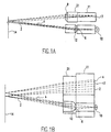
- FIG. 1A is an optical design schematic of an integrated assembly including a light source 10, a transmit diffractive optical element (DOE) 6, a transmit refractive lens 12, a return refractive lens 8 and a detector 17. These elements are integrated onto transparent substrates. Light output by the light source 10 is split into a plurality of light beams by the DOE 6. These beams are delivered to a target surface 14 via the transmit refractive lens 12. In FIG. 1A, two beams 2, 4 are shown as an example, although any number may be used. These beams are reflected by the target surface to the detector 17 via the return refractive lens 8.
- the detector may include more than one detector, one for each beam, or a single detector with unique areas designated for each beam.
- the light source is a laser
- it is preferably the semiconductor laser chip itself, i.e., not a laser inside a can as typically provided for a macroscopic system. Since the dimensions of the integrated system are much smaller than those for a conventional macroscopic system, the light source must be fairly close to the DOE 6, so that the beam will not be too large thereon and all of the beam will be received by the DOE 6.
- part of the integrated approach of the present invention preferably includes providing the laser chip or die itself adjacent to a transparent substrate.
- the first design was to attempt to simply scale down a macroscopic design.
- a single lens was placed in the return path, as shown in FIG. 1A.
- this lens in the return path provides both separation to the beams as well as focussing thereof in order to properly deliver them to the detector.
- the light from the light source 10 is delivered to the DOE on the top surface of the substrate 11 at a distance from the light source 10. This distance is used to advantage to provide an adequately wide beam at the DOE.
- the beams formed by the DOE are focused on surface 14 located at a distance from the lens 12. This distance is chosen to achieve adequate spot size modulation depth and depth of focus at the media surface.
- the refractive lens 8 is located at a distance d2 from the target and the detector 17 is located a distance d1 from the refractive lens 8.
- the distances d1, d2 are dictated by the substrates 11, 21 on which these elements are mounted.
- the ratio of the distances d1/d2 determines the amount of demagnification of the image reflected from the media that occurs in a lens. In using a single lens in the return path, this demagnification affects not only spot size but spot spacing. Assuming, for example, a spot size of 0.020 mm on the target 14, a demagnification of 1/4 gives a spot size of 0.005 mm which because of aberration is spread to an area 0.025 mm.
- the spacing of the spots is demagnified to 0.025 mm and significant crosstalk noise results. This can be seen by the overlapping beams in the plane of the detector 17 in FIG. 1A.
- the overlapping of the beams also occurs at the return refractive lens 8.
- the return refractive lens 8 In order for the refractive lens to image the beams at a point at which they are sufficiently separated such that the beams will be distinguishable on the detector 17, the return refractive lens 8 would have to be placed closer to the target 14. However, such positioning would destroy the desired integrated nature of the optical apparatus.
- the angles of the beams 2, 4 need to be as small as possible and as similar as possible, so that these beams may both impinge upon a central portion of the return refractive lens 8.
- the angle of beam 2 is 5.6 degrees and the angle of beam 4 is 6.9 degrees.
- the beams 2, 4 also need to be sufficiently separated on the detector 17.
- FIG. 1B is an alternative configuration created by recognizing that by providing larger angles to the light beams and providing greater difference between the angles of the light beams, the need for an optical element in the return path could be eliminated.
- the separation between the light beams 2,4 in FIG. 1B is sufficient such that the beams remain separate and distinguishable on the detector 17 without requiring an optical element in the return path to provide this separation.
- the angle of beam 2 is 8 degrees and the angle of beam 4 is 11 degrees.
- FIG. 1B the distance between the top surfaces of the top substrates and the target 14 is the same as it was in FIG. 1A. This clearly results in the beams being further separated on the target 14. For many applications, this increased separation is not a problem, but for those for which a particular separation is desired, the integrated optical head can be positioned closer to the target 14.
- FIG. 1B While the configuration shown in FIG. 1B is advantageous for integrated apparatuses, for many applications, the complete elimination of optical elements in the return path results in an unacceptable level of noise.
- a solution, an example of which is shown in FIG 1C is to include separate optical elements for each beam in the return path. The ability to use more than one optical element in the return path can be realized due to the increased separation between the beams. The feasibility of such a solution, requiring more than one optical element for each beam, is facilitated by the passive alignment discussed in detail below.
- FIG. 1C is an optical design schematic of an assembly according to the invention for use in, for example, detecting an optical track on a storage media.
- a light source 10 directs coherent light, with a dispersion angle of fifteen degrees, upward through an object distance d1 through a diffractive element (DOE) not shown and to a refractive lens 12.
- DOE diffractive element
- the DOE divides the light into a number of beams, only three of which are shown as a plurality of rays in FIG. 1C.
- the beams are focused on surface 14 located at an image distance from the lens 12.
- the spot size and spacing of the light on the image surface 14 determines the tracking accuracy and therefore the amount of information that can be stored on the media.
- the size to which the spot can be reduced is in the instant design, approximately 0.020 mm.
- the refractive lens 12 must have a significant curvature in order to focus the light to 0.020 mm spots on the media.
- the spots of light are spaced approximately 0.100 mm from each other on the media to limit crosstalk noise.
- the optical head can be positioned by the illustrated positioning means 29.
- all optical elements needed to create the more than one beam, direct the beams onto the target and direct the beams from the target to the detector are on the substrate and/or any structure bonded thereto, thereby providing an integrated optical apparatus.
- any optical elements in both the return path and the transmit path are less than 500 microns in diameter, more preferably, less than 300 microns in diameter.
- the actual size of the elements will be dictated by the overall size of the device with which the integrated optical apparatus is to be used, with a lower practical limit being on the order of a wavelength.
- the lens curvature required to focus the laser light to 0.020 mm spots in this compact architecture would control the dimensions of the single lens.
- the use of a single lens as taught in the prior art for reducing the size of optical heads is a limiting factor in size reduction of the entire optical head assembly. This factor is one of the reasons that multiple lenses are employed in the instant invention instead of a single lens.
- the use of multiple lenses is enabled by having the separation between the beams be sufficient so that each beam is incident only on one of the lenses in the return path.
- the ratio of the distances d1/d2 determines the amount of demagnification of the image reflected from the media that occurs in a lens. In a single lens design, this demagnification affects not only spot size but spot spacing. A demagnification of 1/4 gives a spot size of 0.005 mm which because of aberration is spread to an area 0.025 mm. If a single lens design had been used, the spacing of the spots would also have been demagnified to 0.025 mm and significant crosstalk noise would result. By using individual lenses, spaced approximately 0.200 mm, the detectors can be spaced at about 0.220 mm and thereby eliminate crosstalk noise using the 0.025 mm light spots.
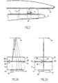
- FIG. 2 is a side view of a magnetic floppy disk head 5 with an optical tracking assembly according to an example.
- Head 5 is mounted, in arm 3 by known means not shown, for the extension across the various tracks of media 14.
- Head 5 is electrically connected to read and write circuits and tracing control circuits by a flexible printed circuit 7.
- a recess 9 of approximately two millimeters by one point six millimeters and four and a half or five millimeters deep is provided in head 5 in which the optical assembly comprising substrate 11 is mounted and connected to flexible printed circuit 7. It will be appreciated that the same assembly techniques and methods may be used to assemble optical disk read heads, as well as magnetic disk heads with optical tracking.
- a first transparent substrate 11 comprising fused silica or other optical material has component mounting metalized pads or contact pads placed on its bottom surface 13, such as using substrate fiducial marks or indicia and accurately aligned photolithographic masks and metal deposition steps known in the art of microelectronic circuit manufacture.
- surface 13 of substrate 11 is approximately 1.6 mm by 2 mm and the substrate 11 is approximately 0.8 mm thick.
- a laser chip 15 is mounted to the surface 13 by means of some of the mentioned metalized pads.
- laser 15 is an edge emitting laser with the laser light directed upwards through means of a precision mirror 33 as shown in FIG. 4. It will by understood that the edge emitting laser 15 can be replaced with a vertical cavity surface emitting laser and thereby obviate the need for the precision mirror in order to direct the laser beam normal to the substrate surface.
- An optical detector chip 17 is also mounted to the component surface of substrate 11 by means of the metalized pads.
- a hologram surface 19 on the opposite side of substrate 11 carries the diffractive optical elements shown in detail in FIG. 7.
- the diffractive optical element phase profiles are designed using the computer calculations and manufactured using techniques taught by Swanson et al. in U.S. Patent 5,161,059, the entire disclosure of which is incorporated herein by reference.
- the optical elements are created photolithographically using the same fiducial marks or indicia used to place the metalized pads. Alternately second fiducial marks that have been aligned with the first marks may be used to align the masks that are also used to create the optical elements. In this way, when the light source, mirror and detector are mounted on their metalized pads, the optical paths among the devices and through the optical elements are in optical alignment as shown more clearly in FIGS. 3A and 3B.
- the precision mirror if needed for redirecting light from an edge emitting laser, is considered to be a device for the purposes of this description only because of the way it is mounted using metalized pads and solder as a silicon chip would be mounted.
- the hologram surface 19 also has the attachment areas 23 that attach the first transparent substrate 11 with a second transparent substrate 21.
- the second substrate 21 carries the refractive optics in a surface 25 that provides the second lens of lens pairs or doublets.
- Light from laser 15 is shaped and split by a diffractive optical element in hologram surface 19 into five separate beams of light that are directed through substrate and travel approximately 2.4 mm to the media. Only the chief ray of each beam is shown in FIG. 3 for clarity of the description.
- One beam is used for intensity feedback to control the electrical power to laser 15.
- the other four beams are used for media position or tracking detection.
- the beams of coherent light are reflected from media 14 and return through second substrate 21 and first substrate 11 to be detected by detector 17.
- the elements are all in their designed optical alignment by virtue of the placement of the metalization pads, there is no need to energize the laser and move the elements relative to each other to bring them into optical alignment. In other words, passive alignment is used rather than the active alignment requiring operation of the laser as in the prior art. It will be recognized that although the beams preferably pass first through the diffractive optical element in surface 19, the order of the optical elements in the light path could be changed or the elements could be combined into one more complex element.
- FIG. 3B is another side view of the assembly of FIG. 3A.
- the light emitted by edge emitting laser 15 comes out substantially parallel to the plane of component surface 13 and must be directed normal to the component surface by the 45 degree surface of mirror 33.
- the light can then pass through substrate 11, a diffractive optical element in surface 19, a refractive lens 61 in surface 25, substrate 21 and be reflected from media 14 as shown in FIGS. 1A-1C and 3A.
- FIG. 4A is a plan top view of the component surface 13 looking down through transparent substrate 11. Electrical contact metalizations 39, 41, 43 and 45 provide electrical connections to detecting photo-diodes in detector 17. Centered under detector 17 is a metalized area 53 having three apertures through which light reflected from media 14 is received. Solder ball alignment areas 47 on each side of area 53 serve both as electrical contacts and as alignment mechanisms in this embodiment. The areas 49 are also solder balls or pads which serve to align and connect the laser 15 to the first substrate and provide current to laser 15. Areas 51 on the other hand only provide mechanical alignment and mechanical attachment of mirror 33 to first transparent substrate 11.
- the hologram surface 19 appears in FIG. 4B in plan view, again looking down onto substrate 11.
- Hologram surface 19 has metalized area 55 which acts as a mask to reduce stray light but allow three beams created by diffractive optics from the light from laser to be directed to media 14 from which they are reflected to reach detector 17 through the five apertures shown in metalized areas 59.
- metalized area 55 Surrounding metalized area 55 is a diffraction grating 57 that scatters stray light from laser 15 so that it does not adversely affect detector 17.
- FIG. 4C shows the refractive lens surface 25, again in plan view looking down, this time through substrate 21.
- Lens 61 in combination with the diffractive optical elements in mask 55 shape and focus the laser light into three spots of approximately 20 Am diameter and spaced at approximately 100 microns onto media 14.
- Lenses 63 and 65 focus the light reflected from media 14 through mask 59 to detector 17 for position control and/or reading.
- Lens 67 focuses reflected light to the photo-diode of detector 17 that provides an intensity level signal to the power control circuits which control the electrical power provided to laser 15.
- Surrounding both surface 19 and surface 25 is an attachment area shown generally as area 71 in FIGS. 4B and 4C.
- Area 71 contains spacing stand off benches and is the area in which an adhesive is placed in order to join substrate 21.
- the standoffbenches passively define a proper or desired vertical spacing or alignment.
- the adhesive is ultraviolet light cured adhesive that can be laid down without concern for time to harden.
- the adhesive is placed in areas 71 and then after the substrates 11 and 21 are aligned, the assembly is flooded with ultra-violet light to catalyze the adhesive.
- the adhesive is replaced with photolithographically placed metalization pads and the two substrates are joined using solder ball technology.
- FIG. 4B also shows three diffractive optical elements 73, 75 with mask 55. These three elements 35 provide the five beams of light to be reflected from the media, the three main rays of which are shown in FIG. 3A.
- Element 75 provides the power control beam that is reflected from the media and is received at aperture 79 in mask 59 as shown in FIG. 8.
- Elements 73 and 77 each provide two beams that interfere at the media surface to create a dark band with two light bands on either side of the dark bands. The light bands are reflected back down to the pairs of apertures 81, 83 and 85, 87 shown in FIG. 4C to provide the varying light intensity that is used to detect an optical track on the media.
- the apertures 73, 75 and 77 containing diffractive elements are each approximately 100 microns long and 20 microns wide.
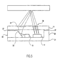
- FIG. 5 illustrates an alternative to providing separate refractive elements in each return path.
- each refractive element in the return path has been replaced with a diffractive element 39.
- the refractive element in the transmit path has also been replaced with a diffractive element 37 for splitting radiation output by the radiation source 15, and delivered to the diffractive element 37 via the precision mirror 33.
- the diffractive element 37 provides separation to the beams delivered to the grating on the surface 14.
- the use of diffractive elements in the return path is typically not as advantageous as refractive elements.
- the diffractive elements are more wavelength dependent and less efficient for larger angles.
- the active elements are mounted on a support substrate 31, preferably a silicon substrate.
- This support substrate 31 also serves as a heat sink for the active elements mounted thereon.
- Attachment areas 23 separate the substrate 31 from the substrate 11 on which the diffractive elements 37, 39 are mounted.
- the active elements may be mounted support substrate 31 using passive alignment in a similar manner as discussed above regarding the mounting of these elements on the transparent substrate 11.
- the attachment areas 23 can be provided by etching a recess into the support substrate 31 in which the laser 15, the detector 17, and the optional mirror 33 may be provided. In other words, the unetched portions of the substrate 31 serve as attachment areas 23.
- the substrates 11, 31 may then be bonded with solder material 27.
- an angled sidewall of the substrate adjacent the recess therein can serve as the mirror 33.
- the attachment areas 23 may include spacer block separate from the substrate 31, as shown in FIGS. 6 and 7.
- the mirror 33 can be a separate element from the spacer blocks, as shown in FIG. 6 or can itself serve as a spacer block, as shown in FIG. 7.
- an embodiment of the present invention is directed to employing no optical elements in the return path.
- the diffractive element 37 in the transmit path is designed to provide sufficient spread to the radiation such that the beams incident on the detector 17 are still distinguishable. This is facilitated by the provision of a refractive element 19 on an opposite surface of the substrate 11 from the diffractive element.
- FIG. 7 illustrates another embodiment in which no optical elements are used in the transmit path.
- the refractive element 19 is mounted opposite the diffractive element 37 on a further substrate 21.
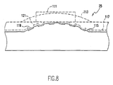
- a refractive optical element in the form of a microlens 115 is formed by placing a circular layer of photoresist 111 on a surface of optical material using a mask. The photoresist is then partially flowed using controlled heat so that the photoresist assumes a partially spherical shape 113. Thereafter, the surface 25 is etched and a refractive element 115 having substantially the same shape as the photoresist 113 is formed by the variable etch rate of the continuously varying thickness of the photoresist 113.
- the microlens 115 is further processed by etching or embossing steps.
- a layer of photoresist 117 is placed over the microlens 115 and exposed through a photolithographic mask with the phase pattern of a diffractive optical element.
- the exposed photoresist is then developed, the surface ofthe microlens can be further etched with the diffractive optical element pattern to produce a hybrid optical element 119.
- a polymer is placed over the microlens in place of the photoresist and the phase pattern is embossed into the polymer as shown at 121.
- the single surface hybrid element 119 is preferably used in the transmit path, for example, in place of the two surface hybrid element shown in FIG. 6.
- all of the substrates may be passively aligned and attached using patterns formed photolithographically as discussed below. While the following discussion references the transparent substrates 11, 21, the support substrate 31 may also be aligned in an analogous fashion.
- the integrated optical apparatuses shown in FIGS. 5-7 may be formed by passively aligning a support wafer having a plurality of active elements thereon with a transparent wafer having a corresponding plurality of optical elements. This support-transparent wafer pair may then be diced apart. Alternatively, the support wafer can be diced and individual laser/detector assemblies aligned and attached to the transparent wafer such as by flip-chip attachment. By first forming individual active assemblies, the lasers can be tested separately.
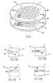
- FIG. 9 shows the two transparent substrates 11 and 21 prior to their being assembled into optical assemblies and diced. Because each element has been accurately placed on each substrate using photolithography, the entire wafers can be aligned and joined prior to being diced into chips without the need to energize any of the laser devices on the substrate 11.
- FIG. 9 shows the substrates inverted from the way they are shown in FIGS. 2, 3A and 3B in order to show the lasers, mirrors and detectors in place on top of each die. Of course, if the support substrate 31 being aligned with one or both of the transparent substrates, to form the configurations shown in FIGS. 5-7, these active elements are not on the top of the wafer 11.
- the adhesive material e.g., ultra-violet curable solder
- the adhesive material e.g., ultra-violet curable solder
- the two wafers are placed one above the other and aligned.
- a known photolithographic mask aligning tool is used with vernier fiduciary marks 93 and 95 to monitor the relative displacement of the two substrates until they are in alignment with each other.
- the substrate 11 can then be lowered onto substrate 21, the alignment rechecked, and the adhesive catalyzed by ultraviolet light.
- the two wafers are passively aligned using mechanical mating elements 91.
- Three forms of mechanical mating elements are contemplated and shown in FIGS. 10A, 10B and 10C.
- One, shown in FIG. 10A takes the form of V-shaped grooves 97 etched into matching faces of the substrates 11 and 21. These grooves are then aligned with sphere 99 to index the two wafers into alignment. Note that only a few grooves and spheres are needed to align all of the dies while they are still together as a wafer.
- Another embodiment of the alignment means shown in FIG. 10B, comprises photolithographically placed metalization pads 101 which are then connected by reflowing a solder ball 103.
- the metalization pads 101 may be solder, without the need for the solder ball 103.
- a bench 105 is raised by etching the surrounding surface and the bench 105 is indexed into a recess 107, also created by photolithographically placed etchant, preferably reactive ion etchant.
- each die means may be needed to accurately space the two substrates from each other. Spacing is accomplished in one embodiment by means of a bench 109 shown in FIG. 10D. Three or more benches 109 are located in the area 71 around each die in an adhesive with high compressive. In another embodiment, the solder bumps or balls and metalizations are used in area 23 accomplishing both attachment and alignment as shown in FIG. 10B. Alternately, when an adhesive with high compressive strength is chosen, only three or more such benches are needed for spacing the entire wafers and after the adhesive has set, the joined wafers can be diced without substrate spacing.
- the diffractive optical elements may be placed on the same surface of a substrate on which the electronic components are accurately placed with these diffractive optical elements using photolithography.
- refractive optical elements may be placed using photolithography in alignment on the other surface of the same substrate thereby allowing an entire optical assembly to be fabricated using but one substrate without the need for actively energizing a light source in the assembly to accomplish alignment.
Landscapes
- Physics & Mathematics (AREA)
- Optics & Photonics (AREA)
- General Physics & Mathematics (AREA)
- Semiconductor Lasers (AREA)
- Optical Head (AREA)
- Diffracting Gratings Or Hologram Optical Elements (AREA)
- Optical Couplings Of Light Guides (AREA)
- Geophysics And Detection Of Objects (AREA)
- Photometry And Measurement Of Optical Pulse Characteristics (AREA)
- Analysing Materials By The Use Of Radiation (AREA)
Claims (33)
- Integrierte optische Vorrichtung, enthaltend:dadurch gekennzeichnet, dass sich alle optischen Elemente, die notwendig sind, um die mehr als einen Strahl umfassenden Strahlen zu erzeugen und um diese mehr als einen Strahl umfassenden Strahlen auf das Ziel (14) zu richten, auf dem ersten Substrat (21) und/oder einer beliebigen Struktur, die an das erste Substrat (21) gebondet ist, befinden, wobei keine optischen Elemente in einem. Rücklaufweg von dem Ziel (14) zu der Erfassungseinrichtung (17) vorhanden sind und wobei der Rücklaufweg durch das erste Substrat (21) verläuft.ein erstes Substrat (21), welches optisch transparent ist und eine erste sowie eine zweite Fläche aufweist, die einander gegenüberliegen;eine Lichtquelle (15), die zu dem ersten Substrat (21) benachbart angeordnet ist, um Licht durch das erste Substrat (21) in Richtung auf ein entferntes Ziel (14) abzustrahlen;ein optisches Übertragungssystem auf dem ersten Substrat (21), das in einem optischen Übertragungsweg von der Lichtquelle (15) zu dem Ziel (14) angeordnet ist und das das Licht in mehr als einen Strahl aufteilt; undeine Erfassungseinrichtung (17), welche diese mehr als einen Strahl umfassenden Strahlen, die durch das Ziel (14) reflektiert werden, empfängt,
- Vorrichtung nach Anspruch 1, bei der die Erfassungseinrichtung (17) mehr als ein Lichterfassungselement zum Erfassen eines entsprechenden Strahls der mehr als einen Strahl umfassenden Strahlen enthält, die von dem entfernten Ziel (14) reflektiert werden, wobei das optische Übertragungssystem eine ausreichende Trennung zwischen den mehr als einen Strahl umfassenden Strahlen bereitstellt, so dass jeder Strahl dieser mehr als einen Strahl umfassenden Strahlen zu einem entsprechenden eindeutigen Lichterfassungselement der mehr als einen Erfassungselement umfassenden Erfassungselemente zugeführt wird.
- Vorrichtung nach Anspruch 1, bei der das optische Übertragungssystem ein lichtbrechendes/lichtbeugendes Hybridelement ist.
- Vorrichtung nach Anspruch 3, wobei das Hybridelement aus einer einzelnen Oberfläche des Substrats (21) gebildet ist.
- Vorrichtung nach Anspruch 3, bei der ein lichtbrechender Abschnitt des Hybridelements an der ersten Fläche des ersten Substrats (21) und ein lichtbeugender Abschnitt des Hybridelements an der zweiten Fläche des ersten Substrats (21) ausgebildet ist.
- Vorrichtung nach Anspruch 1, weiterhin enthaltend Mittel zum Montieren der Stahlenabgabeeinrichtung und der Erfassungseinrichtung (17) auf dem ersten Substrat (21).
- Vorrichtung nach Anspruch 1, weiterhin enthaltend:ein Trägersubstrat, wobei die Lichtquelle (15) und die Erfassungseinrichtung (17) auf dem Trägersubstrat angebracht sind; undein Mittel zum Zusammenbonden des Trägersubstrats und des ersten Substrats (21).
- Vorrichtung nach Anspruch 7, bei der das Mittel zum Bonden Distanzstücke zwischen dem ersten Substrat (21) und dem Trägersubstrat enthält.
- Vorrichtung nach Anspruch 1, bei der die integrierte optische Vorrichtung ein Positionssensor ist, der verwendet wird, um die Position des Sensors gegenüber dem entfernt liegenden Ziel (14) zu bestimmen.
- Vorrichtung nach Anspruch 1, bei der Lichtquelle (15) ein Laser mit Kantenstrahlung ist, wobei die Vorrichtung weiterhin einen Spiegel enthält, der zum Zurückführen von Licht von dem Laser mit Kantenstrahlung verwendet wird und der zu dem ersten Substrat (21) benachbart angeordnet ist.
- Vorrichtung nach Anspruch 1, bei der die Lichtquelle (15) ein vertikaler Hohlraumlaser mit Oberflächenemission.
- Vorrichtung nach Anspruch 1, weiterhin enthaltend ein mechanisch zueinander passendes Mittel zum passiven Ausrichten von zumindest der Lichtquelle (15) oder der Erfassungseinrichtung (17) gegenüber dem ersten Substrat (21).
- Vorrichtung nach Anspruch 12, bei der das mechanisch zueinander passende Mittel Distanzstücke enthält, um eine präzise Trennung zwischen der Lichtquelle (15) und dem Substrat bereitzustellen.
- Vorrichtung nach Anspruch 1, bei der das erste Substrat (21) weiterhin zumindest ein Metallkissen auf einer Bodenfläche des Substrats enthält, welches verwendet wird, um die Positionierung von zumindest der Lichtquelle (15) oder der Erfassungseinrichtung (17) zu unterstützen.
- Vorrichtung nach Anspruch 14, weiterhin enthaltend ein Lötkissen auf der Oberseite von zumindest einem Metallkissen.
- Vorrichtung nach Anspruch 1, bei der die Lichtquelle (15) ein Halbleiter-Laserchip ist, der direkt an das erste Substrat (21) gebondet ist.
- Vorrichtung nach Anspruch 1, bei der die Lichtquelle (15) ein Halbleiter-Laserchip ist, der mittels Distanzstücken an das Substrat gebondet ist.
- Vorrichtung nach Anspruch 2, bei der die mehr als ein Lichterfassungselement umfassenden Lichterfassungselemente mehr als einen Bereich auf einer einzelnen Erfassungseinrichtung enthalten.
- Vorrichtung nach Anspruch 1, bei der die beliebige Struktur, die an das erste Substrat (21) gebondet ist, enthält:ein zweites Substrat, welches optisch transparent ist und welches optische Elemente des optischen Übertragungssystems, welche darauf integriert sind, aufweist; undein Mittel zum Zusammenbonden des zweiten Substrats und des ersten Substrats (21).
- Vorrichtung nach Anspruch 19, bei der das Mittel zum Bonden Distanzstücke zwischen dem ersten Substrat (21) und dem zweiten Substrat aufweist.
- Vorrichtung nach Anspruch 19, weiterhin enthaltend ein optisch beugendes Element auf einer oberen Oberfläche des ersten Substrats (21) und ein optisch brechendes Element auf einer unteren Oberfläche des zweiten Substrats.
- Vorrichtung nach Anspruch 1, bei der das optische Übertragungssystem ein einzelnes optisch beugendes Element ist.
- Vorrichtung nach Anspruch1, bei der das optisch Übertragungssystem eine Vielzahl an optisch beugenden Elementen enthält.
- Vorrichtung nach Anspruch 1, bei der die optischen Elemente in dem optischen Übertragungssystem Durchmesser von weniger als 50 µm aufweisen.
- Vorrichtung nach Anspruch 1, weiterhin enthaltend Metallabschnitte, die auf dem Substrat (21i) in zumindest dem Übertragungsweg oder einem Rücklaufweg von dem Ziel (14) zu der Erfassungseinrichtung (17) photolitographisch erzeugt sind und die als eine Maske dienen.
- Verfahren zum Integrieren einer optischen Vorrichtung, enthaltend:Montieren einer Lichtquelle (15), die zu einem ersten Substrat (21) benachbart angeordnet ist, wobei das erste Substrat (21) optisch transparent ist und wobei die Lichtquelle (15) vorgesehen ist, Licht durch das erste Substrat (21) in Richtung auf ein entferntes Ziel (14) abzustrahlen;Bereitstellen eines optischen Übertragungssystems auf dem ersten Substrat (21), welches in einem optischen Übertragungsweg von der Lichtquelle (15) zu dem Ziel (14) positioniert ist und welches das Licht in mehr als einen Strahl aufteilt;Montieren einer Erfassungseinrichtung (17) benachbart zu dem ersten Substrat (21), wobei die Erfassungseinrichtung (17) zum Empfangen der mehr als einen Strahl umfassenden Strahlen, die durch das Ziel (14) reflektiert werden, vorgesehen ist; undBereitstellen eines Rücklaufweges von dem Ziel (14) zu der Erfassungseinrichtung (17) über das erste Substrat (21), wobei der Rücklaufweg keine optischen Elemente enthält; undBereitstellen aller optischen Elemente, die notwendig sind, mehr als einen Strahl zu erzeugen und diese mehr als einen Strahl umfassenden Strahlen auf das Ziel (14) auszurichten, auf dem ersten Substrat (21) und/oder einer beliebigen Struktur, die an dem ersten Substrat (21) gebondet ist.
- Verfahren nach Anspruch 26, bei dem zumindest das Bereitstellen der Lichtquelle (15) oder das Bereitstellen der Lichterfassungseinrichtung das passive Ausrichten mit dem ersten Substrat (21) enthält.
- Verfahren nach Anspruch 26, weiterhin enthaltend:Anordnen der Lichtquelle (15) und der Erfassungseinrichtung (17) auf einem Trägersubstrat und Zusammenbonden des Trägersubstrats und des ersten Substrats (21).
- Verfahren nach Anspruch 26, weiterhin enthaltend das Zusammenbonden eines zweiten Substrats und des ersten Substrats (21), wobei das zweite Substrat optisch transparent ist und optische Elemente des optischen Übertragungssystems aufweist.
- Verfahren nach Anspruch 26, weiterhin enthaltend das photolitographische Ausbilden von Metallabschnitten auf dem ersten Substrat (21) in einem Rücklaufweg von dem Ziel (14) zu der Erfassungseinrichtung (17), wobei die Metallabschnitte als eine Maske dienen.
- Verfahren nach Anspruch 26, weiterhin enthaltend präzises Trennen der Lichtquelle (15) und des Substrats über Distanzstücke.
- Verfahren nach Anspruch 26, weiterhin enthaltend das Bereitstellen von zumindest einem Metallkissen auf einer unteren Fläche des ersten Substrats (21), um die Positionierung von zumindest der Lichtquelle (15) oder der Erfassungseinrichtung (17) zu unterstützen.
- Verfahren nach Anspruch 26, weiterhin enthaltend das Bereitstellen eines Lötkissens auf dem zumindest einem Metallkissen.
Priority Applications (1)
| Application Number | Priority Date | Filing Date | Title |
|---|---|---|---|
| EP03004782A EP1324324A3 (de) | 1998-02-05 | 1999-02-01 | Integriertes optisches Gerät zur Erzeugung von getrennten Strahlen auf einem Detektor und zugehöriges Verfahren |
Applications Claiming Priority (3)
| Application Number | Priority Date | Filing Date | Title |
|---|---|---|---|
| US18891 | 1998-02-05 | ||
| US09/018,891 US5912872A (en) | 1996-09-27 | 1998-02-05 | Integrated optical apparatus providing separated beams on a detector and associated methods |
| PCT/US1999/001887 WO1999040578A1 (en) | 1998-02-05 | 1999-02-01 | Integrated optical apparatus providing separated beams on a detector and associated methods |
Related Child Applications (1)
| Application Number | Title | Priority Date | Filing Date |
|---|---|---|---|
| EP03004782A Division EP1324324A3 (de) | 1998-02-05 | 1999-02-01 | Integriertes optisches Gerät zur Erzeugung von getrennten Strahlen auf einem Detektor und zugehöriges Verfahren |
Publications (2)
| Publication Number | Publication Date |
|---|---|
| EP1053545A1 EP1053545A1 (de) | 2000-11-22 |
| EP1053545B1 true EP1053545B1 (de) | 2003-04-09 |
Family
ID=21790296
Family Applications (2)
| Application Number | Title | Priority Date | Filing Date |
|---|---|---|---|
| EP99904399A Expired - Lifetime EP1053545B1 (de) | 1998-02-05 | 1999-02-01 | Integriertes optisches gerät zur erzeugung von getrennten strahlen auf einem detektor, und zugehörige verfahren |
| EP03004782A Ceased EP1324324A3 (de) | 1998-02-05 | 1999-02-01 | Integriertes optisches Gerät zur Erzeugung von getrennten Strahlen auf einem Detektor und zugehöriges Verfahren |
Family Applications After (1)
| Application Number | Title | Priority Date | Filing Date |
|---|---|---|---|
| EP03004782A Ceased EP1324324A3 (de) | 1998-02-05 | 1999-02-01 | Integriertes optisches Gerät zur Erzeugung von getrennten Strahlen auf einem Detektor und zugehöriges Verfahren |
Country Status (8)
| Country | Link |
|---|---|
| US (3) | US5912872A (de) |
| EP (2) | EP1053545B1 (de) |
| JP (1) | JP2002503011A (de) |
| AT (1) | ATE237179T1 (de) |
| AU (1) | AU2480399A (de) |
| CA (1) | CA2319420C (de) |
| DE (1) | DE69906704T2 (de) |
| WO (1) | WO1999040578A1 (de) |
Families Citing this family (92)
| Publication number | Priority date | Publication date | Assignee | Title |
|---|---|---|---|---|
| US6235141B1 (en) | 1996-09-27 | 2001-05-22 | Digital Optics Corporation | Method of mass producing and packaging integrated optical subsystems |
| US5912872A (en) * | 1996-09-27 | 1999-06-15 | Digital Optics Corporation | Integrated optical apparatus providing separated beams on a detector and associated methods |
| US6327110B1 (en) * | 1997-03-21 | 2001-12-04 | Matsushita Electric Industrial Co., Ltd. | Optical system, position detecting apparatus, magnetic recording apparatus, and lens with aperture |
| JP3017718B1 (ja) * | 1998-09-29 | 2000-03-13 | 松下電送システム株式会社 | 基板およびこれを用いた画像記録装置 |
| US7208725B2 (en) * | 1998-11-25 | 2007-04-24 | Rohm And Haas Electronic Materials Llc | Optoelectronic component with encapsulant |
| US6348358B1 (en) * | 1999-02-19 | 2002-02-19 | Presstek, Inc. | Emitter array with individually addressable laser diodes |
| US20070181781A1 (en) | 2001-03-06 | 2007-08-09 | Digital Optics Corporation | Integrated optical transceiver |
| US20040041081A1 (en) | 2002-08-30 | 2004-03-04 | Feldman Michael R. | Integrated optical transceiver and related methods |
| JP2003526909A (ja) * | 2000-03-06 | 2003-09-09 | ディジタル・オプティックス・コーポレイション | 集積化された光トランシーバおよび関連方法 |
| US7842914B2 (en) | 2000-03-06 | 2010-11-30 | Tessera North America, Inc. | Optoelectronic package, camera including the same and related methods |
| US6631113B1 (en) * | 2000-10-04 | 2003-10-07 | Dphi Acquisitions, Inc. | Continuous flexible connection method for miniature optical head |
| US7054256B2 (en) * | 2000-10-20 | 2006-05-30 | Ochoa Optics Llc | High capacity digital data storage by transmission of radiant energy through arrays of small diameter holes |
| US6807131B1 (en) * | 2000-12-27 | 2004-10-19 | Research Investment Network, Inc. | Near-field hybrid magnetic-optical head system |
| US7078671B1 (en) | 2001-08-06 | 2006-07-18 | Shipley Company, L.L.C. | Silicon optical microbench devices and wafer-level testing thereof |
| JP2003101063A (ja) * | 2001-09-20 | 2003-04-04 | Sony Corp | 複合光学素子、受光素子装置及び複合光学素子の製造方法 |
| US7194561B2 (en) | 2001-10-12 | 2007-03-20 | Sonics, Inc. | Method and apparatus for scheduling requests to a resource using a configurable threshold |
| US6804738B2 (en) | 2001-10-12 | 2004-10-12 | Sonics, Inc. | Method and apparatus for scheduling a resource to meet quality-of-service restrictions |
| US6578117B2 (en) | 2001-10-12 | 2003-06-10 | Sonics, Inc. | Method and apparatus for scheduling requests using ordered stages of scheduling criteria |
| US6961834B2 (en) * | 2001-10-12 | 2005-11-01 | Sonics, Inc. | Method and apparatus for scheduling of requests to dynamic random access memory device |
| US7224856B2 (en) * | 2001-10-23 | 2007-05-29 | Digital Optics Corporation | Wafer based optical chassis and associated methods |
| US7961989B2 (en) * | 2001-10-23 | 2011-06-14 | Tessera North America, Inc. | Optical chassis, camera having an optical chassis, and associated methods |
| JP3743359B2 (ja) * | 2001-11-30 | 2006-02-08 | 松下電器産業株式会社 | 光ピックアップ装置 |
| US7006426B2 (en) * | 2001-12-18 | 2006-02-28 | Stmicroelectronics, Inc. | Integrated optical unit for use with miniature optical discs |
| US6977780B2 (en) * | 2001-12-27 | 2005-12-20 | Fuji Photo Film Co., Ltd. | Image exposure device and laser exposure device applied thereto |
| US7129508B2 (en) * | 2002-01-18 | 2006-10-31 | Honeywell International Inc. | Compact VCSEL sensor with multiple sensing capabilities |
| US7343535B2 (en) * | 2002-02-06 | 2008-03-11 | Avago Technologies General Ip Dte Ltd | Embedded testing capability for integrated serializer/deserializers |
| AU2003226601A1 (en) * | 2002-04-16 | 2003-10-27 | Xloom Photonics Ltd. | Electro-optical circuitry having integrated connector and methods for the production thereof |
| US20040021214A1 (en) * | 2002-04-16 | 2004-02-05 | Avner Badehi | Electro-optic integrated circuits with connectors and methods for the production thereof |
| US7180929B2 (en) * | 2002-04-18 | 2007-02-20 | Intel Corporation | Wafer-level test structure for edge-emitting semiconductor lasers |
| WO2004029948A1 (de) * | 2002-09-20 | 2004-04-08 | Osram Opto Semiconductors Gmbh | Optischer abtastkopf und verfahren zur herstellung desselben |
| DE10253907A1 (de) * | 2002-09-20 | 2004-04-01 | Osram Opto Semiconductors Gmbh | Optischer Abtastkopf und Verfahren zur Herstellung desselben |
| US20040071466A1 (en) * | 2002-10-10 | 2004-04-15 | Buckman Lisa A. | Controlled optical splitter using a diffractive optical element and optical demultiplexer incorporating same |
| US6970491B2 (en) * | 2002-10-30 | 2005-11-29 | Photodigm, Inc. | Planar and wafer level packaging of semiconductor lasers and photo detectors for transmitter optical sub-assemblies |
| JP2004246279A (ja) * | 2003-02-17 | 2004-09-02 | Seiko Epson Corp | 光モジュール及びその製造方法、光通信装置、光電気混載集積回路、回路基板、電子機器 |
| EP1611468B1 (de) * | 2003-03-26 | 2008-05-21 | Digital Optics Corporation | Gehäuse für optoelektronisches bauteil auf waferebene |
| KR100612844B1 (ko) | 2003-05-09 | 2006-08-18 | 삼성전자주식회사 | 집적 광픽업 및 그 제조방법 및 이를 구비하는광정보저장장치 |
| US20050063431A1 (en) * | 2003-09-19 | 2005-03-24 | Gallup Kendra J. | Integrated optics and electronics |
| US7520679B2 (en) * | 2003-09-19 | 2009-04-21 | Avago Technologies Fiber Ip (Singapore) Pte. Ltd. | Optical device package with turning mirror and alignment post |
| US6982437B2 (en) * | 2003-09-19 | 2006-01-03 | Agilent Technologies, Inc. | Surface emitting laser package having integrated optical element and alignment post |
| US6953990B2 (en) * | 2003-09-19 | 2005-10-11 | Agilent Technologies, Inc. | Wafer-level packaging of optoelectronic devices |
| US20050063648A1 (en) * | 2003-09-19 | 2005-03-24 | Wilson Robert Edward | Alignment post for optical subassemblies made with cylindrical rods, tubes, spheres, or similar features |
| WO2005036226A1 (en) * | 2003-10-15 | 2005-04-21 | Xloom Photonics Ltd. | Electro-optical circuitry having integrated connector and methods for the production thereof |
| US8504992B2 (en) * | 2003-10-31 | 2013-08-06 | Sonics, Inc. | Method and apparatus for establishing a quality of service model |
| US7665069B2 (en) * | 2003-10-31 | 2010-02-16 | Sonics, Inc. | Method and apparatus for establishing a quality of service model |
| US9087036B1 (en) | 2004-08-12 | 2015-07-21 | Sonics, Inc. | Methods and apparatuses for time annotated transaction level modeling |
| JP2007538347A (ja) * | 2003-11-28 | 2007-12-27 | トムソン ライセンシング | 光電トランスジューサ及び光ピックアップを製造する方法 |
| US20050213995A1 (en) * | 2004-03-26 | 2005-09-29 | Myunghee Lee | Low power and low jitter optical receiver for fiber optic communication link |
| KR100601955B1 (ko) * | 2004-06-01 | 2006-07-14 | 삼성전기주식회사 | 집적 광학 시스템 및 그 제조 방법 및 이를 적용한 정보기록 및/또는 재생기기 |
| US20070223329A1 (en) * | 2004-06-16 | 2007-09-27 | Koninklijke Philips Electronics, N.V. | Apparatus And Method For Generating A Scanning Beam In An Optical Pickup Head, Miniature Optical Pickup Head And Optical Storage System Incorporating A Miniature Pickup Head |
| KR100647300B1 (ko) * | 2004-12-14 | 2006-11-23 | 삼성전기주식회사 | 광학 벤치, 집적 광학 시스템 및 광학 정렬 방법 |
| US7180669B2 (en) * | 2004-12-17 | 2007-02-20 | Avago Technologies Ecbu Ip (Singapore) Pte. Ltd. | Method and system for generating substantially uniform speckle patterns |
| JP2006236516A (ja) * | 2005-02-28 | 2006-09-07 | Hitachi Ltd | 光へッド、光情報再生装置及びその製造方法 |
| US7750356B2 (en) * | 2005-05-04 | 2010-07-06 | Avago Technologies Fiber Ip (Singapore) Pte. Ltd. | Silicon optical package with 45 degree turning mirror |
| US7397571B2 (en) * | 2005-05-26 | 2008-07-08 | Inphase Technologies, Inc. | Methods and systems for laser mode stabilization |
| US20060280096A1 (en) * | 2005-05-26 | 2006-12-14 | Inphase Technologies, Inc. | Erasing holographic media |
| US7675025B2 (en) | 2005-05-26 | 2010-03-09 | Inphase Technologies, Inc. | Sensing absolute position of an encoded object |
| US7466411B2 (en) * | 2005-05-26 | 2008-12-16 | Inphase Technologies, Inc. | Replacement and alignment of laser |
| US20060279819A1 (en) * | 2005-05-26 | 2006-12-14 | Inphase Technologies, Inc. | Laser mode stabilization using an etalon |
| US7480085B2 (en) * | 2005-05-26 | 2009-01-20 | Inphase Technologies, Inc. | Operational mode performance of a holographic memory system |
| US20060281021A1 (en) * | 2005-05-26 | 2006-12-14 | Inphase Technologies, Inc. | Illuminative treatment of holographic media |
| US7633662B2 (en) * | 2005-05-26 | 2009-12-15 | Inphase Technologies, Inc. | Holographic drive head alignments |
| US20060291022A1 (en) * | 2005-05-26 | 2006-12-28 | Inphase Technologies, Inc. | Optical delay line in holographic drive |
| US7742211B2 (en) * | 2005-05-26 | 2010-06-22 | Inphase Technologies, Inc. | Sensing and correcting angular orientation of holographic media in a holographic memory system by partial reflection, the system including a galvano mirror |
| US8305700B2 (en) * | 2005-05-26 | 2012-11-06 | Inphase Technologies, Inc. | Holographic drive head and component alignment |
| US7548358B2 (en) * | 2005-05-26 | 2009-06-16 | Inphase Technologies, Inc. | Phase conjugate reconstruction of a hologram |
| US20060275670A1 (en) * | 2005-05-26 | 2006-12-07 | Inphase Technologies, Inc. | Post-curing of holographic media |
| US7710624B2 (en) * | 2005-05-26 | 2010-05-04 | Inphase Technologies, Inc. | Controlling the transmission amplitude profile of a coherent light beam in a holographic memory system |
| US20070236591A1 (en) * | 2006-04-11 | 2007-10-11 | Tam Samuel W | Method for mounting protective covers over image capture devices and devices manufactured thereby |
| US8868397B2 (en) * | 2006-11-20 | 2014-10-21 | Sonics, Inc. | Transaction co-validation across abstraction layers |
| US8456560B2 (en) * | 2007-01-26 | 2013-06-04 | Digitaloptics Corporation | Wafer level camera module and method of manufacture |
| WO2008133943A1 (en) | 2007-04-24 | 2008-11-06 | Flextronics Ap Llc | Small form factor modules using wafer level optics with bottom cavity and flip chip assembly |
| US20090093137A1 (en) * | 2007-10-08 | 2009-04-09 | Xloom Communications, (Israel) Ltd. | Optical communications module |
| US9419032B2 (en) * | 2009-08-14 | 2016-08-16 | Nanchang O-Film Optoelectronics Technology Ltd | Wafer level camera module with molded housing and method of manufacturing |
| US8582618B2 (en) | 2011-01-18 | 2013-11-12 | Avago Technologies General Ip (Singapore) Pte. Ltd. | Surface-emitting semiconductor laser device in which an edge-emitting laser is integrated with a diffractive or refractive lens on the semiconductor laser device |
| US8315287B1 (en) | 2011-05-03 | 2012-11-20 | Avago Technologies Fiber Ip (Singapore) Pte. Ltd | Surface-emitting semiconductor laser device in which an edge-emitting laser is integrated with a diffractive lens, and a method for making the device |
| CN103620779B (zh) | 2011-07-19 | 2016-12-28 | 赫普塔冈微光有限公司 | 光电模块及其制造方法 |
| SG2014005805A (en) | 2011-08-10 | 2014-06-27 | Heptagon Micro Optics Pte Ltd | Opto-electronic module and method for manufacturing the same |
| JP2013131509A (ja) * | 2011-12-20 | 2013-07-04 | Ricoh Co Ltd | 光学ユニットの製造方法、光学ユニット、光走査装置及び画像形成装置 |
| JP6338533B2 (ja) | 2011-12-22 | 2018-06-06 | ヘプタゴン・マイクロ・オプティクス・プライベート・リミテッドHeptagon Micro Optics Pte. Ltd. | 光電子モジュール、特にフラッシュモジュールおよびそれらの製造方法 |
| WO2013190871A1 (ja) * | 2012-06-20 | 2013-12-27 | アオイ電子株式会社 | 光源一体型光センサ |
| TWI627761B (zh) * | 2012-07-17 | 2018-06-21 | 新加坡恒立私人有限公司 | 用以感測一量度的感測器模組,其應用器具,其製造方法,裝置的製造方法,及包含光譜計模組的裝置 |
| TW201417250A (zh) | 2012-07-17 | 2014-05-01 | 海特根微光學公司 | 光學模組,特別是光電模組,及其製造方法 |
| TWI707483B (zh) * | 2012-07-17 | 2020-10-11 | 新加坡商新加坡恒立私人有限公司 | 發射可變強度分布的光線的光電模組 |
| TW201419505A (zh) * | 2012-07-17 | 2014-05-16 | 海特根微光學公司 | 精巧型光電模組及其製造方法 |
| TW201414992A (zh) * | 2012-07-17 | 2014-04-16 | Heptagon Micro Optics Pte Ltd | 精巧型光譜計模組及其製造方法 |
| TW201415614A (zh) * | 2012-07-17 | 2014-04-16 | Heptagon Micro Optics Pte Ltd | 精巧型光學模組及其製造方法 |
| KR101873132B1 (ko) * | 2013-11-22 | 2018-06-29 | 헵타곤 마이크로 옵틱스 피티이. 리미티드 | 컴팩트 광전자 모듈들 |
| TWI650851B (zh) * | 2013-12-10 | 2019-02-11 | Heptagon Micro Optics Pte. Ltd. | 晶圓級光學模組及其製造方法 |
| JP6459615B2 (ja) * | 2015-02-24 | 2019-01-30 | 住友電気工業株式会社 | 光データリンク |
| US10152992B1 (en) * | 2018-02-09 | 2018-12-11 | Sae Magnetics (H.K.) Ltd. | Light source unit and thermally-assisted magnetic head |
| CN108598863A (zh) * | 2018-05-30 | 2018-09-28 | 华进半导体封装先导技术研发中心有限公司 | 光电器件封装件 |
| CN109273514A (zh) * | 2018-11-02 | 2019-01-25 | 深圳阜时科技有限公司 | 电子设备 |
Family Cites Families (49)
| Publication number | Priority date | Publication date | Assignee | Title |
|---|---|---|---|---|
| US4626103A (en) * | 1984-03-29 | 1986-12-02 | At&T Bell Laboratories | Focus tracking system |
| US4636080A (en) * | 1984-05-07 | 1987-01-13 | At&T Bell Laboratories | Two-dimensional imaging with line arrays |
| DE3536497A1 (de) * | 1984-10-16 | 1986-04-17 | Mitsubishi Denki K.K., Tokio/Tokyo | Vorrichtung zur erfassung von fokussierungsfehlern in einer kopfanordnung fuer optische scheiben |
| US5159586A (en) * | 1985-05-24 | 1992-10-27 | Omron Tateisi Electronics Co. | Device for processing optical data |
| DE3683684D1 (de) * | 1985-05-24 | 1992-03-12 | Omron Tateisi Electronics Co | Vorrichtung zur verarbeitung optischer daten. |
| EP0226647B1 (de) * | 1985-12-17 | 1991-05-29 | Ibm Deutschland Gmbh | Schreib/Lesekopf für optische Platten |
| US5168324A (en) * | 1986-09-25 | 1992-12-01 | The United States Of America As Represented By The United States Department Of Energy | Wavelength meter having elliptical wedge |
| US5189485A (en) * | 1986-09-25 | 1993-02-23 | The United States Of America As Represented By The United States Department Of Energy | Wavelength meter having single mode fiber optics multiplexed inputs |
| US4966446A (en) * | 1989-04-28 | 1990-10-30 | At&T Bell Laboratories | Mask controlled coupling of inter-substrate optical components |
| US5352796A (en) * | 1989-10-30 | 1994-10-04 | The Salk Institute For Biological Studies | Amino acids useful in making GnRH analogs |
| US5025165A (en) * | 1990-03-26 | 1991-06-18 | At&T Bell Laboratories | Method for producing a semiconductor device using an electron beam exposure tool and apparatus for producing the device |
| US5093879A (en) * | 1990-06-22 | 1992-03-03 | International Business Machines Corporation | Electro-optical connectors |
| US5317551A (en) * | 1990-07-16 | 1994-05-31 | Matsushita Electric Industrial Co., Ltd. | Optical disk head including a light path having a thickness and width greater than the light beam wavelength by a predetermined amount |
| US5159473A (en) * | 1991-02-27 | 1992-10-27 | University Of North Carolina | Apparatus and method for programmable optical interconnections |
| US5204516A (en) * | 1991-04-23 | 1993-04-20 | U.S. Philips Corporation | Planar optical scanning head having deficiency-correcting grating |
| US5170269A (en) * | 1991-05-31 | 1992-12-08 | Texas Instruments Incorporated | Programmable optical interconnect system |
| US5229883A (en) * | 1991-10-28 | 1993-07-20 | Mcdonnell Douglas Corporation | Hybrid binary optics collimation fill optics |
| US5202775A (en) * | 1991-11-04 | 1993-04-13 | University Of North Carolina | Radically symmetric hologram and method of fabricating the same |
| US5237434A (en) * | 1991-11-05 | 1993-08-17 | Mcnc | Microelectronic module having optical and electrical interconnects |
| US5276756A (en) * | 1991-12-06 | 1994-01-04 | Amoco Corporation | High speed electro-optical signal translator |
| US5457314A (en) * | 1991-12-31 | 1995-10-10 | Hyundai Electronics Industries Co., Ltd. | Mount for positioning a photodetector on an optical apparatus |
| US5446719A (en) * | 1992-02-05 | 1995-08-29 | Sharp Kabushiki Kaisha | Optical information reproducing apparatus |
| US5410468A (en) * | 1992-06-26 | 1995-04-25 | Matsushita Electric Industrial Co., Ltd. | Optical pick-up apparatus |
| US5309282A (en) * | 1992-07-17 | 1994-05-03 | The United States Of America As Represented By The United States Department Of Energy | High stability wavefront reference source |
| US5856048A (en) * | 1992-07-27 | 1999-01-05 | Dai Nippon Printing Co., Ltd. | Information-recorded media and methods for reading the information |
| DE69318770T2 (de) * | 1992-07-30 | 1998-10-15 | Matsushita Electric Ind Co Ltd | Optisches Wiedergabegerät |
| US5337398A (en) * | 1992-11-30 | 1994-08-09 | At&T Bell Laboratories | Single in-line optical package |
| JP3082516B2 (ja) * | 1993-05-31 | 2000-08-28 | キヤノン株式会社 | 光学式変位センサおよび該光学式変位センサを用いた駆動システム |
| JP2798583B2 (ja) * | 1993-06-08 | 1998-09-17 | 日本電気株式会社 | 光デバイスの製造方法 |
| TW255015B (de) * | 1993-11-05 | 1995-08-21 | Motorola Inc | |
| US5499312A (en) * | 1993-11-09 | 1996-03-12 | Hewlett-Packard Company | Passive alignment and packaging of optoelectronic components to optical waveguides using flip-chip bonding technology |
| JPH07287883A (ja) * | 1994-04-19 | 1995-10-31 | Victor Co Of Japan Ltd | 光集積回路 |
| US5418870A (en) * | 1994-04-28 | 1995-05-23 | Corning Incorporated | Coaxial coupler with integrated source/ring detector |
| JPH07296441A (ja) * | 1994-04-28 | 1995-11-10 | Sony Corp | 光学装置 |
| JP2806293B2 (ja) * | 1994-10-06 | 1998-09-30 | 松下電器産業株式会社 | 光ピックアップ及びその製造方法 |
| JPH08115532A (ja) * | 1994-10-18 | 1996-05-07 | Matsushita Electric Ind Co Ltd | 光集積素子及びそれを用いた集積型光ピックアップ装置及び光ディスク装置 |
| US5648950A (en) * | 1994-10-25 | 1997-07-15 | Kabushiki Kaisha Sankyo Seiki Seisakusho | Hologram integrated with a beam splitter to separate a plurality of polarized reflected light beams |
| JPH08235663A (ja) * | 1995-02-24 | 1996-09-13 | Sony Corp | 光学素子 |
| EP0767953A2 (de) * | 1995-03-29 | 1997-04-16 | Koninklijke Philips Electronics N.V. | Einheit mit strahlungsquelle, detektor und gitter, und abtastvorrichtung mit dieser optischen einheit |
| EP0740294A1 (de) * | 1995-04-26 | 1996-10-30 | Matsushita Electric Industrial Co., Ltd. | Optischer Kopf |
| US5652744A (en) * | 1996-02-08 | 1997-07-29 | Industrial Technology Research Institute | Single surface diffractive element for optical pickup heads |
| JP3732268B2 (ja) * | 1996-02-28 | 2006-01-05 | 富士通株式会社 | 光ディスク装置用光学ヘッド |
| JPH09251663A (ja) * | 1996-03-15 | 1997-09-22 | Toshiba Corp | 光学素子ユニットおよびその製造方法 |
| US5771218A (en) * | 1996-09-27 | 1998-06-23 | Digital Optics Corporation | Passively aligned integrated optical head including light source, detector, and optical element and methods of forming same |
| US5886971A (en) * | 1996-09-27 | 1999-03-23 | Digital Optics Corporation | Optical head structures including support substrates adjacent transparent substrates and related methods |
| US5912872A (en) * | 1996-09-27 | 1999-06-15 | Digital Optics Corporation | Integrated optical apparatus providing separated beams on a detector and associated methods |
| US5910940A (en) * | 1996-10-08 | 1999-06-08 | Polaroid Corporation | Storage medium having a layer of micro-optical lenses each lens generating an evanescent field |
| JP3601219B2 (ja) * | 1996-11-13 | 2004-12-15 | 松下電器産業株式会社 | 光ピックアップ用の平行プリズム |
| JPH10172173A (ja) * | 1996-12-06 | 1998-06-26 | Samsung Electron Co Ltd | 光ピックアップ装置 |
-
1998
- 1998-02-05 US US09/018,891 patent/US5912872A/en not_active Expired - Lifetime
-
1999
- 1999-02-01 EP EP99904399A patent/EP1053545B1/de not_active Expired - Lifetime
- 1999-02-01 AU AU24803/99A patent/AU2480399A/en not_active Abandoned
- 1999-02-01 WO PCT/US1999/001887 patent/WO1999040578A1/en not_active Ceased
- 1999-02-01 EP EP03004782A patent/EP1324324A3/de not_active Ceased
- 1999-02-01 AT AT99904399T patent/ATE237179T1/de not_active IP Right Cessation
- 1999-02-01 DE DE69906704T patent/DE69906704T2/de not_active Expired - Lifetime
- 1999-02-01 JP JP2000530907A patent/JP2002503011A/ja active Pending
- 1999-02-01 CA CA002319420A patent/CA2319420C/en not_active Expired - Fee Related
- 1999-03-23 US US09/274,310 patent/US6104690A/en not_active Expired - Lifetime
-
2000
- 2000-08-15 US US09/637,364 patent/US6522618B1/en not_active Expired - Lifetime
Also Published As
| Publication number | Publication date |
|---|---|
| US6104690A (en) | 2000-08-15 |
| ATE237179T1 (de) | 2003-04-15 |
| DE69906704D1 (de) | 2003-05-15 |
| EP1053545A1 (de) | 2000-11-22 |
| EP1324324A2 (de) | 2003-07-02 |
| US5912872A (en) | 1999-06-15 |
| EP1324324A3 (de) | 2008-10-22 |
| CA2319420A1 (en) | 1999-08-12 |
| JP2002503011A (ja) | 2002-01-29 |
| DE69906704T2 (de) | 2004-03-04 |
| WO1999040578A1 (en) | 1999-08-12 |
| CA2319420C (en) | 2002-12-24 |
| AU2480399A (en) | 1999-08-23 |
| US6522618B1 (en) | 2003-02-18 |
Similar Documents
| Publication | Publication Date | Title |
|---|---|---|
| EP1053545B1 (de) | Integriertes optisches gerät zur erzeugung von getrennten strahlen auf einem detektor, und zugehörige verfahren | |
| US5771218A (en) | Passively aligned integrated optical head including light source, detector, and optical element and methods of forming same | |
| US5886971A (en) | Optical head structures including support substrates adjacent transparent substrates and related methods | |
| WO1998013825A9 (en) | Integrated optical head apparatus and associated methods | |
| US8153957B2 (en) | Integrated optical imaging systems including an interior space between opposing substrates and associated methods | |
| US20080136955A1 (en) | Integrated camera and associated methods | |
| JP4221513B2 (ja) | 集積型ビーム整形器およびその使用方法 | |
| EP0555097B1 (de) | Gerät zur Wiedergabe optischer Information | |
| US6542281B2 (en) | Integrated micro-optical systems | |
| KR20030088427A (ko) | 광학 헤드를 위한 빔세이퍼 | |
| KR100955355B1 (ko) | 박형 광학 헤드 | |
| CN100392736C (zh) | 小型光头 | |
| US6522619B2 (en) | Optical pick-up device having a plurality of light sources with different calorific values and method of manufacturing the same | |
| US6922425B2 (en) | Semiconductor laser device and optical pickup device | |
| JPH11203706A (ja) | 光学ヘッド及びその製造方法 | |
| US20120094066A1 (en) | Integrated micro-optical systems and cameras including the same | |
| US6671236B2 (en) | Light receiving and emitting compound element and optical pick-up device using the same | |
| US8059345B2 (en) | Integrated micro-optical systems | |
| JP3457982B2 (ja) | 光半導体装置並びにその製造方法 | |
| JP3518904B2 (ja) | 光ピックアップ | |
| JPH04121827A (ja) | 焦点検出装置 | |
| JPH08212586A (ja) | 光ピックアップ装置及びその製造方法 |
Legal Events
| Date | Code | Title | Description |
|---|---|---|---|
| PUAI | Public reference made under article 153(3) epc to a published international application that has entered the european phase |
Free format text: ORIGINAL CODE: 0009012 |
|
| 17P | Request for examination filed |
Effective date: 20000905 |
|
| AK | Designated contracting states |
Kind code of ref document: A1 Designated state(s): AT BE CH CY DE DK ES FI FR GB GR IE IT LI LU MC NL PT SE |
|
| AX | Request for extension of the european patent |
Free format text: AL PAYMENT 20000905;LT PAYMENT 20000905;LV PAYMENT 20000905;MK PAYMENT 20000905;RO PAYMENT 20000905;SI PAYMENT 20000905 |
|
| 17Q | First examination report despatched |
Effective date: 20010216 |
|
| GRAG | Despatch of communication of intention to grant |
Free format text: ORIGINAL CODE: EPIDOS AGRA |
|
| GRAG | Despatch of communication of intention to grant |
Free format text: ORIGINAL CODE: EPIDOS AGRA |
|
| GRAH | Despatch of communication of intention to grant a patent |
Free format text: ORIGINAL CODE: EPIDOS IGRA |
|
| GRAH | Despatch of communication of intention to grant a patent |
Free format text: ORIGINAL CODE: EPIDOS IGRA |
|
| GRAA | (expected) grant |
Free format text: ORIGINAL CODE: 0009210 |
|
| AK | Designated contracting states |
Designated state(s): AT BE CH CY DE DK ES FI FR GB GR IE IT LI LU MC NL PT SE |
|
| AX | Request for extension of the european patent |
Extension state: AL LT LV MK RO SI |
|
| PG25 | Lapsed in a contracting state [announced via postgrant information from national office to epo] |
Ref country code: NL Free format text: LAPSE BECAUSE OF FAILURE TO SUBMIT A TRANSLATION OF THE DESCRIPTION OR TO PAY THE FEE WITHIN THE PRESCRIBED TIME-LIMIT Effective date: 20030409 Ref country code: LI Free format text: LAPSE BECAUSE OF FAILURE TO SUBMIT A TRANSLATION OF THE DESCRIPTION OR TO PAY THE FEE WITHIN THE PRESCRIBED TIME-LIMIT Effective date: 20030409 Ref country code: IT Free format text: LAPSE BECAUSE OF FAILURE TO SUBMIT A TRANSLATION OF THE DESCRIPTION OR TO PAY THE FEE WITHIN THE PRESCRIBED TIME-LIMIT;WARNING: LAPSES OF ITALIAN PATENTS WITH EFFECTIVE DATE BEFORE 2007 MAY HAVE OCCURRED AT ANY TIME BEFORE 2007. THE CORRECT EFFECTIVE DATE MAY BE DIFFERENT FROM THE ONE RECORDED. Effective date: 20030409 Ref country code: FI Free format text: LAPSE BECAUSE OF FAILURE TO SUBMIT A TRANSLATION OF THE DESCRIPTION OR TO PAY THE FEE WITHIN THE PRESCRIBED TIME-LIMIT Effective date: 20030409 Ref country code: CY Free format text: LAPSE BECAUSE OF FAILURE TO SUBMIT A TRANSLATION OF THE DESCRIPTION OR TO PAY THE FEE WITHIN THE PRESCRIBED TIME-LIMIT Effective date: 20030409 Ref country code: CH Free format text: LAPSE BECAUSE OF FAILURE TO SUBMIT A TRANSLATION OF THE DESCRIPTION OR TO PAY THE FEE WITHIN THE PRESCRIBED TIME-LIMIT Effective date: 20030409 Ref country code: BE Free format text: LAPSE BECAUSE OF FAILURE TO SUBMIT A TRANSLATION OF THE DESCRIPTION OR TO PAY THE FEE WITHIN THE PRESCRIBED TIME-LIMIT Effective date: 20030409 Ref country code: AT Free format text: LAPSE BECAUSE OF FAILURE TO SUBMIT A TRANSLATION OF THE DESCRIPTION OR TO PAY THE FEE WITHIN THE PRESCRIBED TIME-LIMIT Effective date: 20030409 |
|
| REG | Reference to a national code |
Ref country code: GB Ref legal event code: FG4D |
|
| REG | Reference to a national code |
Ref country code: CH Ref legal event code: EP |
|
| REG | Reference to a national code |
Ref country code: IE Ref legal event code: FG4D |
|
| PG25 | Lapsed in a contracting state [announced via postgrant information from national office to epo] |
Ref country code: SE Free format text: LAPSE BECAUSE OF FAILURE TO SUBMIT A TRANSLATION OF THE DESCRIPTION OR TO PAY THE FEE WITHIN THE PRESCRIBED TIME-LIMIT Effective date: 20030709 Ref country code: PT Free format text: LAPSE BECAUSE OF FAILURE TO SUBMIT A TRANSLATION OF THE DESCRIPTION OR TO PAY THE FEE WITHIN THE PRESCRIBED TIME-LIMIT Effective date: 20030709 Ref country code: GR Free format text: LAPSE BECAUSE OF FAILURE TO SUBMIT A TRANSLATION OF THE DESCRIPTION OR TO PAY THE FEE WITHIN THE PRESCRIBED TIME-LIMIT Effective date: 20030709 Ref country code: DK Free format text: LAPSE BECAUSE OF FAILURE TO SUBMIT A TRANSLATION OF THE DESCRIPTION OR TO PAY THE FEE WITHIN THE PRESCRIBED TIME-LIMIT Effective date: 20030709 |
|
| ET | Fr: translation filed | ||
| NLV1 | Nl: lapsed or annulled due to failure to fulfill the requirements of art. 29p and 29m of the patents act | ||
| LTIE | Lt: invalidation of european patent or patent extension |
Effective date: 20030409 |
|
| REG | Reference to a national code |
Ref country code: CH Ref legal event code: PL |
|
| PG25 | Lapsed in a contracting state [announced via postgrant information from national office to epo] |
Ref country code: ES Free format text: LAPSE BECAUSE OF FAILURE TO SUBMIT A TRANSLATION OF THE DESCRIPTION OR TO PAY THE FEE WITHIN THE PRESCRIBED TIME-LIMIT Effective date: 20031030 |
|
| PG25 | Lapsed in a contracting state [announced via postgrant information from national office to epo] |
Ref country code: LU Free format text: LAPSE BECAUSE OF NON-PAYMENT OF DUE FEES Effective date: 20040201 |
|
| PG25 | Lapsed in a contracting state [announced via postgrant information from national office to epo] |
Ref country code: IE Free format text: LAPSE BECAUSE OF NON-PAYMENT OF DUE FEES Effective date: 20040202 |
|
| PLBE | No opposition filed within time limit |
Free format text: ORIGINAL CODE: 0009261 |
|
| STAA | Information on the status of an ep patent application or granted ep patent |
Free format text: STATUS: NO OPPOSITION FILED WITHIN TIME LIMIT |
|
| PG25 | Lapsed in a contracting state [announced via postgrant information from national office to epo] |
Ref country code: MC Free format text: LAPSE BECAUSE OF NON-PAYMENT OF DUE FEES Effective date: 20040228 |
|
| RAP2 | Party data changed (patent owner data changed or rights of a patent transferred) |
Owner name: DIGITAL OPTICS CORPORATION |
|
| 26N | No opposition filed |
Effective date: 20040112 |
|
| REG | Reference to a national code |
Ref country code: IE Ref legal event code: MM4A |
|
| REG | Reference to a national code |
Ref country code: FR Ref legal event code: CD |
|
| REG | Reference to a national code |
Ref country code: FR Ref legal event code: CD Owner name: DIGITALOPTICS CORPORATION EAST, US Effective date: 20120111 |
|
| REG | Reference to a national code |
Ref country code: DE Ref legal event code: R082 Ref document number: 69906704 Country of ref document: DE Representative=s name: EISENFUEHR, SPEISER & PARTNER, DE |
|
| REG | Reference to a national code |
Ref country code: DE Ref legal event code: R082 Ref document number: 69906704 Country of ref document: DE Representative=s name: EISENFUEHR SPEISER PATENTANWAELTE RECHTSANWAEL, DE Effective date: 20120217 Ref country code: DE Ref legal event code: R081 Ref document number: 69906704 Country of ref document: DE Owner name: FLIR SYSTEMS TRADING BELGIUM BVBA, BE Free format text: FORMER OWNER: TESSERA NORTH AMERICA .INC. (N. D. GES. D. STAATES DELAWARE), CHARLOTTE, N.C., US Effective date: 20120217 |
|
| REG | Reference to a national code |
Ref country code: DE Ref legal event code: R082 Ref document number: 69906704 Country of ref document: DE Representative=s name: EISENFUEHR SPEISER PATENTANWAELTE RECHTSANWAEL, DE |
|
| REG | Reference to a national code |
Ref country code: GB Ref legal event code: 732E Free format text: REGISTERED BETWEEN 20140911 AND 20140917 |
|
| REG | Reference to a national code |
Ref country code: DE Ref legal event code: R082 Ref document number: 69906704 Country of ref document: DE Representative=s name: EISENFUEHR SPEISER PATENTANWAELTE RECHTSANWAEL, DE Effective date: 20140904 Ref country code: DE Ref legal event code: R081 Ref document number: 69906704 Country of ref document: DE Owner name: FLIR SYSTEMS TRADING BELGIUM BVBA, BE Free format text: FORMER OWNER: DIGITALOPTICS CORPORATION EAST (N. D. GES. D. STAATES DELAWARE), CHARLOTTE, N.C., US Effective date: 20140904 |
|
| REG | Reference to a national code |
Ref country code: FR Ref legal event code: PLFP Year of fee payment: 17 |
|
| PGFP | Annual fee paid to national office [announced via postgrant information from national office to epo] |
Ref country code: DE Payment date: 20150305 Year of fee payment: 17 |
|
| PGFP | Annual fee paid to national office [announced via postgrant information from national office to epo] |
Ref country code: GB Payment date: 20150226 Year of fee payment: 17 Ref country code: FR Payment date: 20150226 Year of fee payment: 17 |
|
| REG | Reference to a national code |
Ref country code: DE Ref legal event code: R119 Ref document number: 69906704 Country of ref document: DE |
|
| GBPC | Gb: european patent ceased through non-payment of renewal fee |
Effective date: 20160201 |
|
| REG | Reference to a national code |
Ref country code: FR Ref legal event code: ST Effective date: 20161028 |
|
| PG25 | Lapsed in a contracting state [announced via postgrant information from national office to epo] |
Ref country code: GB Free format text: LAPSE BECAUSE OF NON-PAYMENT OF DUE FEES Effective date: 20160201 Ref country code: FR Free format text: LAPSE BECAUSE OF NON-PAYMENT OF DUE FEES Effective date: 20160229 Ref country code: DE Free format text: LAPSE BECAUSE OF NON-PAYMENT OF DUE FEES Effective date: 20160901 |