EP1053632B1 - Teilnehmeranschlussschnittstellenschaltung - Google Patents
Teilnehmeranschlussschnittstellenschaltung Download PDFInfo
- Publication number
- EP1053632B1 EP1053632B1 EP98955607A EP98955607A EP1053632B1 EP 1053632 B1 EP1053632 B1 EP 1053632B1 EP 98955607 A EP98955607 A EP 98955607A EP 98955607 A EP98955607 A EP 98955607A EP 1053632 B1 EP1053632 B1 EP 1053632B1
- Authority
- EP
- European Patent Office
- Prior art keywords
- voltage
- subscriber line
- interface circuit
- control
- subscriber
- Prior art date
- Legal status (The legal status is an assumption and is not a legal conclusion. Google has not performed a legal analysis and makes no representation as to the accuracy of the status listed.)
- Expired - Lifetime
Links
Images


Classifications
-
- H—ELECTRICITY
- H04—ELECTRIC COMMUNICATION TECHNIQUE
- H04M—TELEPHONIC COMMUNICATION
- H04M19/00—Current supply arrangements for telephone systems
- H04M19/001—Current supply source at the exchanger providing current to substations
- H04M19/005—Feeding arrangements without the use of line transformers
-
- H—ELECTRICITY
- H04—ELECTRIC COMMUNICATION TECHNIQUE
- H04M—TELEPHONIC COMMUNICATION
- H04M3/00—Automatic or semi-automatic exchanges
- H04M3/005—Interface circuits for subscriber lines
Definitions
- the invention relates to a subscriber line in a telephone system.
- FIG. 1 shows an analog subscriber interface 15 which can be located in a multiplexing unit 14 arranged separately from the exchange 10, the multiplexing unit being connected to a digital subscriber interface 19 of the exchange via a digital link 18 (of e.g. 2 Mbit/s).
- This kind of a remote multiplexing unit 16 can also be connected via a digital link 20 (of e.g. 2 Mbit/s) to another multiplexing unit 21 located close to the exchange.
- An analog subscriber interface 221 of the other multiplexing unit is connected, in turn, to an analog subscriber interface 23 in a digital or an analog exchange.
- Multiplexers and digital connections used as described above support longer distances between subscribers and an exchange than a purely analog subscriber line.
- a multiplexer can be placed close to the subscribers, which allows a subscriber network to be implemented in a star configuration of short subscriber lines and, thereby, at relatively low cabling costs.
- FIG. 2 The principle of a subscriber line interface of a digital exchange is shown in Figure 2.
- Wires a and b of an analog subscriber line are connected to a subscriber line interface circuit 30 (SLIC). Audio frequencies appearing on the wires a and b are routed to the SLIC 30 which sets a termination impedance of the subscriber line and separates transmit and receive direction signals from one another.
- a receive direction signal is supplied via a low-pass filter 31 to a codec 33 which converts the analog signal of the subscriber line into a digital PCM coded form and transfers the PCM signal further to the exchange.
- a PCM coded signal arriving from the exchange is converted in the codec 33 into an analog transmit direction signal, which is supplied to the subscriber line via a low-pass filter 32 and the SLIC 30.
- a subscriber line interface circuit SLIC comprises power supply to the subscriber line, ring voltage supply, detection of subscriber loop activation (off-hook), etc.
- An active subscriber loop, or off-hook is a situation in which the subscriber has lifted the handset from its holder and an associated switch connects the a and b wires of the subscriber line together, a direct current loop being thereby formed from the SLIC via the subscriber line to the subscriber terminal, and back.
- the SLIC detects the loop current and informs the exchange about the off-hook state.
- the subscriber loop opens and the loop current disappears.
- the SLIC detects that there is no loop current and informs the on-hook state to the exchange.
- the distances of the subscribers from the exchange vary greatly. Some of the subscribers may be very close to the exchange, within 50-500 m, for example, while others may be several kilometers away from it. For this reason the length of the subscriber lines also varies, thereby causing variation in subscriber loop resistance. Further variation in subscriber loop resistance is caused by subscriber terminal type, subscriber line characteristics, the number of subscriber terminals connected to a subscriber line, etc.
- One of the requirements concerning a subscriber line interface is that the loop current must be substantially constant irrespective of the total resistance and dissipation in the subscriber loop.
- the output stage of the subscriber line interface circuit, which supplies the loop current, must therefore be provided with a loop current control.
- An object of the present invention is to provide a simple and inexpensive subscriber line interface circuit comprising a control function maintaining a constant loop current.
- a subscriber line interface circuit to be connected to a bi-directional, two-wire subscriber line for the transfer of audio signals and for power supply, the subscriber line interface circuit comprising an output amplifier stage providing supply voltage to the subscriber line; and loop current detector means for measuring the loop current said supply voltage causes in the subscriber loop formed by the subscriber line and a subscriber terminal when the subscriber terminal is in an off-hook state.
- SLIC subscriber line interface circuit
- the circuit of the invention is characterized in that said output amplifier stage comprises a first, non-inverting amplifier, having an input connected to a reference voltage and to a control voltage, and an output connected to a first wire of the subscriber line; and a second, inverting amplifier, having a first input connected to a reference voltage, a second input connected to a control voltage, and an output connected to a second wire of the subscriber line, said first and second amplifiers being arranged to provide, according to said control voltage, a first and a second output voltage, which are of an equal magnitude but have opposite signs with respect to a subscriber line average voltage determined by said reference voltage; said detector means comprise means for measuring a first current in the first subscriber line wire and a second current in the second subscriber line wire, and for producing a sum of the first and the second measurement results; and that the subscriber line interface circuit also comprises a control means responsive to said sum of the measurement results for changing the control voltage, at the beginning of an off-hook state, with a predetermined time constant, thereby
- the output stage of the subscriber line interface circuit comprises two amplifiers, one of which is configured to operate as an inverting amplifier (negative amplification) and the other one as a non-inverting amplifier (positive amplification).
- the output of each amplifier is connected to a respective subscriber line wire.
- a common reference voltage and a common control voltage are supplied to both amplifiers.
- the reference voltage sets amplifier output voltages of the lowest control voltage level substantially at an average voltage, or symmetry point, between the subscriber line supply voltage and ground. With a minimum control voltage, the output of both amplifiers is at the average voltage and there is no voltage difference between the subscriber lines.
- the voltage of the first amplifier changes from the average voltage towards ground potential and the output voltage of the second amplifier towards the supply voltage, or vice versa, depending on the control voltage potential. Consequently, as the amplifier output voltages increase symmetrically in relation to the average voltage, voltage difference between the subscriber line wires also increases which, in turn, increases subscriber loop current.
- Loop current is measured from each wire of the subscriber line and the results are summed together, a common mode interference possibly appearing being thereby cancelled.
- the sum of the measurement results is thus directly proportional to the loop current value.
- the sum of the measurement results is supplied to the control means, the output voltage of which is the control voltage of the first and the second amplifiers. If the loop current is too high, the control means changes the control voltage, with a predetermined time constant, to a direction decreasing the output voltages of the amplifiers. This makes also the voltage difference between the subscriber line wires smaller, thereby reducing the loop current.
- the control voltage provided by the control means is set at the voltage level thus obtained.
- control sets the loop current to suit a particular subscriber loop resistance and dissipation, and it also adapts to slow changes in the subscriber loop characteristics.
- the control loop filters off rapid changes measured in the loop current and caused by momentary disturbances or by an alternating voltage audio signal transferred over the subscriber line.
- the control means is an integrator.
- the control loop is provided with a voltage limiter which, in order to allow an alternating voltage information signal to be transferred over the subscriber line in an on-hook state, limits the maximum control voltage of the on-hook state to a level ensuring that the maximum output voltages of the first and the second amplifiers are at a predetermined voltage offset from ground and from an operating voltage potential. A voltage offset of some volts is preferred. Without the limiter, the control voltage provided by the integrator would increase in an on-hook state (because loop current is missing, being thus less than said threshold value) to the level of said reference voltage, whereby the output voltages of the amplifiers would be controlled to operating voltage and ground potentials.
- the voltage limiter limits the maximum control voltage to a level that is lower than the reference voltage by an amount equal to a predetermined voltage margin, which corresponds to a desired voltage margin of the output voltages.
- Information transfer taking place in an on-hook state can be used, for example, for transferring a calling subscriber's telephone number to a subscriber terminal and for displaying the number on the subscriber terminal's display before the subscriber answers the call.
- the control loop is provided with a polarity reversal circuit, which supplies the control voltage to the amplifiers at a first polarity or at a second, reversed polarity, depending on the state of a polarity control signal supplied by a telephone exchange.
- a polarity reversal circuit which supplies the control voltage to the amplifiers at a first polarity or at a second, reversed polarity, depending on the state of a polarity control signal supplied by a telephone exchange.
- the power source which provides the operating voltage and said reference voltage for the first and the second amplifiers is arranged to change the amplifier operating voltage according to the amplifier output voltage needed for generating a desired loop current. Since the loop current is substantially constant, the output voltage needed for generating the loop current principally depends on subscriber loop resistance; a high loop resistance requires a high amplifier output voltage. When the loop resistance is low, a low amplifier output voltage is required. The difference between the amplifier operating voltage and output voltage is lost in the form of power dissipation in the amplifiers.
- Power sources may have two or more operating voltages, for example, from which a suitable voltage for a particular loop resistance is selected.
- the power source is responsive to said control voltage, thereby allowing a suitable operating voltage to be selected for the amplifier.
- This is advantageous because the control voltage level is directly proportional to amplifier output voltage.
- the power source can be arranged to supply a first, lower operating voltage when the control voltage level is lower than the predetermined threshold value, and a second, higher operating voltage when the control voltage level exceeds said threshold value, and a second, higher operating voltage when the control voltage level exceeds said threshold value.
- Some telephone systems require, in addition, a particularly high operating voltage for a subscriber line in an on-hook situation.
- the power source can be arranged to only supply the high operating voltage when the subscriber line is in an on-hook state, and to use lower operating voltages for an off-hook state.
- the power source is arranged to set said reference voltage on the basis of the operating voltage in such a way that the average voltage remains at a correct level.
- a subscriber line interface circuit of the present invention can be applied to analog subscriber interfaces, in digital or analog exchanges or in separate multiplexers.
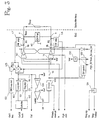
- FIG. 3 illustrates a subscriber line interface circuit (SLIC) of the preferred embodiment of the invention.
- the output stage of the subscribe line interface circuit comprises two amplifiers 110 and 111, the outputs of which are coupled to respective wires a and b of the subscriber line (subscriber loop).
- the amplifier 111 is configured to operate as an inverting amplifier (negative amplification -G) and the amplifier 110 is configured to operate as a non-inverting amplifier (positive amplification G).
- a common reference voltage Vref and a common control voltage Vc are supplied to both amplifiers 110 and 111. At the lowest control voltage Vc level (0 volts), the reference voltage Vref sets output voltages Va and Vb of the amplifiers 110 and 111 substantially at an average voltage (e.g.
- Nom_SV/2 Nom_SV/2
- a minimum control voltage Vc (0 V)
- the output of both amplifiers 110 and 111 is at said average voltage and there is no voltage difference between the subscriber wires a and b.
- the amplifier control voltage Vc increases (> 0 V)
- the output voltage Vb of the amplifier 111 changes from the average voltage towards ground potential and the output voltage Va of the amplifier 110 towards the supply voltage, or vice versa, depending on the polarity of the control voltage Vc. Consequently, as the amplifier output voltages Va and Vb increase symmetrically in relation to the average voltage, voltage difference between the subscriber line wires a and b also increases, thereby increasing loop current lloop in the subscriber loop.
- Speech information from a signal input IN is also supplied to both amplifiers 110 and 111.
- Figure 3 shows, for the sake of clarity, separate inputs for speech and for control voltage, in practice they can be summed to one and the same input through resistors.
- the loop current lloop is separately measured from the wires a and b by means of serial resistors R1 and R2 and differential amplifiers 117 and 118.
- the output voltage of the differential amplifier 117 is proportional to a voltage generated across the resistor R1 by the loop current lloop.
- the output voltage of the differential amplifier 118 is proportional to a voltage generated across the resistor R2 by the loop current lloop.
- the measured voltages are summed in a summing device 119 (such as an operational amplifier) and the summed voltage Vs is supplied to an integrator 126 and to detectors 120 and 121.
- the summation of the measurement voltages is used for cancelling any common mode interference possibly appearing in the subscriber line, the summed voltage Vs thus being directly proportional to the value of the loop current lloop.
- the summed voltage Vs is supplied to the integrator that generates a control voltage V1, the maximum level of which is limited in a limiter 127.
- the control voltage V1 is then supplied to a polarity reversal circuit, the output of which is the control voltage Vc of the amplifiers 110 and 111.
- Figure 4 is a circuit diagram illustrating the integrator 126, limiter 127 and polarity reversal circuit 128 of the preferred embodiment of the invention.
- the circuit involves one integrated circuit IC1, or quad-operational amplifier LM324S.
- the integrator 126 comprises an operational amplifier IC1/1, resistors R8 and R9, capacitor C2 and diode D1.
- the voltage limiter 127 comprises an operational amplifier IC1/2, capacitors C3, C4 and C5, resistors R3, R4 and R7, and a voltage divider formed by resistors R5 and R6.
- the summed voltage Vs is substantially zero.
- the voltage V1 of an output terminal 1 of the operational amplifier IC1/2 connected as the integrator is then substantially the same as the portion of the reference voltage Vref formed by the voltage divider R5 and R6, i.e. K*Vref, where K ⁇ 1.
- the maximum level of the control voltage V1, and thereby that of the control voltage Vc, is thus limited to the voltage K*Vref.
- the voltage K*Vref also appears across the capacitor C2.
- a voltage margin dV (preferably of 1 to 3 V) is left both between the output voltage Va and the supply voltage -48V and between the output voltage Vb and ground, so as to allow information transfer in an on-hook state, as will be described below.
- Decrease in the loop current lloop reduces the summed voltage Vs in the input terminal 2 of the operational amplifier lC1/2.
- the control loop thus reduces the loop current and the voltages Vs and Vc in this way until the summed voltage Vs reaches a threshold value which corresponds to the desired loop current lloop.
- the threshold value is set by means of the resistors R3 and R4.
- the level of the control voltage Vc and the output voltages va and Vb are locked, as shown between t2-t3 in Figure 5.
- the subscriber loop opens, the loop current lloop is cut off and the summed voltage Vs drops to zero.
- the voltage across the capacitor C2, and thereby the control voltage Vc then start to rise again towards the value K*Vref, which is reached at a moment t4.
- the output voltages Va and Vb rise similarly to their maximum values.
- the voltage limiter 127 limits the maximum control voltage to a level at which the maximum output voltages Va and Vb of the amplifiers 110 and 111 are at a predetermined voltage offset dV from ground and from the supply voltage potential, so as to allow an alternating voltage information signal to be transferred over the subscriber line in the on-hook state.
- a voltage offset dV of some volts is preferred.
- Figure 3 shows that information to be transferred in the on-hook state can be supplied to the inputs of the amplifiers 110 and 111 via the signal input In, similarly as speech in an off-hook state, for example.
- the information is in the form of an amplitude modulation of the amplifier output voltages, as illustrated by sine waves 51 and 52 in Figure 5.
- the information transmitted by the subscriber terminal is in the form of a similar voltage modulation, which can be detected by the differential amplifiers 117 and 118.
- the received information is then transmitted to a signal output Out via capacitor C1.
- Information transfer in the on-hook state may be applied for instance for transferring a calling subscriber's telephone number to a subscriber terminal and for displaying the number on the subscriber terminal's display before the subscriber answers the call.
- the polarity reversal circuit 128 supplies the control voltage Vc to the amplifiers 110 and 111 in a conventional manner by applying the above described polarity, the polarities of the output voltages Va and Vb thus being also as shown in Figure 5.
- the telephone exchange can, however, control the circuit 128 so that it reverses the polarity of the control signal Vc, and thereby the polarities of the output voltages Va and Vb.
- polarity reversal would mean that the voltages Va and Vb would momentarily exchange places with one another. This offers a simple way of providing polarity reversal which some telephone systems use for signalling from an exchange to a subscriber terminal over a subscriber line.
- FIG. 4 is a circuit diagram of the preferred embodiment of the invention illustrating the polarity reversal circuit 128.
- the polarity reversal circuit 128 comprises an operational amplifier IC1/3, transistor Q1, resistors R10, R11, R12, R13, R14 and R15, and capacitor C6.
- the transistor Q1 switches the operational amplifier IC1/3 to operate either as a non-inverting amplifier or an inverting amplifier, depending on the state of the control signal Polarity Reversal. When the control signal Polarity Signal is '0', the transistor Q1 does not conduct. This means that the IC1/3 operates as a non-inverting amplifier and allows the control signal Vc to pass through without polarity reversal.
- the transistor Q1 When the control signal Polarity Reversal is '1', the transistor Q1 conducts and couples the +input of the amplifier IC1/3 to ground. In this case the IC1/3 operates as an inverting amplifier and reverses the polarity of the control signal Vc.
- the power source 129 which provides the operating voltage for the amplifiers 110 and 111 is arranged to change the amplifier operating voltage according to the amplifier output voltages Va and Vb needed for generating the desired loop current lloop. Since the loop current lloop is substantially constant, the voltage Va-Vb needed for generating the loop current lloop principally depends on the resistance Zloop of the subscriber loop; a high loop resistance Zloop requires high amplifier output voltages Va-Vb. When the loop resistance Zloop is low, low amplifier output voltages Va-Vb are required. The difference between the operating voltage and the output voltages Va and Vb of the amplifiers 110 and 111 is lost in the form of power dissipation in the amplifiers.
- the operating voltage being reduced when a lower amplifier output voltage is needed, allows amplifier power dissipation and, thereby, power consumption to be reduced.
- the power source 129 can have two or more operating voltages, for example, from which a voltage suitable for a particular loop resistance is selected.
- the power source 129 provides three different operating voltages: normal voltage Nom_SV (e.g. - 48V), high voltage High_SV (e.g. -60V) and low voltage Low_SV (e.g. -30V).
- normal voltage Nom_SV e.g. - 48V
- high voltage High_SV e.g. -60V
- low_SV e.g. -30V
- telephone systems require, in addition, a particularly high supply voltage (about -60V) for a subscriber line in the on-hook state.
- the power source 129 supplies to the amplifiers 110 and 111 the operating voltage High_SV when the subscriber line is in the on-hook state.
- the power source 129 supplies, as shown in Figure 5, the operating voltage Nom_SV (e.g. -48V) in the on-hook state.
- the power source 129 is controlled by means of the control voltage Vc. This is advantageous, because the level of the control voltage Vc is directly proportional to the output voltages Va and Vb of the amplifiers 110 and 111.
- the control voltage Vc When the control voltage Vc is close to Vref, the subscriber line is in the on-hook state and the power source 129 supplies Nom_SV or High_SV.
- the power source 128 supplies Nom_SV.
- the level of the control voltage Vc in the off-hook state exceeds the predetermined threshold value, the power source 128 supplies Low_SV.
- Va is less than -30V between t2-t3, which would allow the operating voltage Low_SV to be used and, consequently, power consumption to be reduced.
- a voltage down-conversion circuit 130 generates the reference voltage Vref from the operating voltage produced by the power source 129.
- the Vref thus always sets according to the operating voltage in such a way that the average voltage remains at a correct level.
- an overvoltage protector unit 112 protecting the subscriber line interface circuit from overvoltage possibly coming over the subscriber line.
- the information signal i.e. a current signal
- the information signal is converted into voltage form in the resistors R1 and R2 and transferred to the summing unit 119 via the amplifiers 117 and 118.
- the current being measured from both ends of a subscriber line Z1 and the results being summed together, a common mode interference signal possibly appearing in the subscriber line can be cancelled.
- the signal is transferred to the Out terminal via a switching capacitor C1.
- the subscriber line interface circuit further comprises an input Ring Voltage, to which a ring signal is supplied.
- the ring signal is activated by activating a switching device 124 through a control input in Ring sig. On so that the ring signal is transferred to the subscriber line wire b.
- the amplifier 111 can be controlled to a high-impedance state through a control input High Ohm.
- the summed voltage coming from the summing unit 119 is also transferred to detector units 120 and 121.
- the detector unit 120 detects if the subscriber line changes from an on-hook state to an off-hook state, i.e. if the line is activated.
- the detector unit 121 detects the change from an on-hook state to an off-hook state when the ring signal is active.
- Information about the state of the subscriber line is further transferred from the detector units 120 and 121 to an output On/Off hook through a selector unit 125.
- the selector unit 125 selects which one of the detector units is to be used.
- the selection takes place on the basis of the signal coming from the control input High Ohm; an active High Ohm signal indicates that the ring signal is also active, so the detector unit 121 will be used. Otherwise the detector unit 120 is used.
- the switching also comprises a detector 122 which is used for detecting a ground key signal and for transferring the signal to a GND key pin.
- the detector 122 receives supply information from the amplifiers 117 and 118 through a subtraction unit 123.
Landscapes
- Engineering & Computer Science (AREA)
- Signal Processing (AREA)
- Power Engineering (AREA)
- Interface Circuits In Exchanges (AREA)
- Devices For Supply Of Signal Current (AREA)
Claims (12)
- Teilnehmeranschluss-Schnittstellenschaltung (SLIC), die eingerichtet ist, zur Übermittlung von Audiosignalen und zur Energieversorgung mit einem bidirektionalen Zweidraht-Teilnehmeranschluss verbunden zu sein, wobei die Teilnehmeranschluss-Schnittstellenschaltung aufweist:eine Ausgangsverstärkerstufe (110, 111) zum Bereitstellen einer Versorgungsspannung an den Teilnehmeranschluss;Schleifenstrom-Detektoreinrichtungen (R1, R2, 117, 118, 119) zum Messen des Schleifenstroms, den die Versorgungsspannung in der Teilnehmerschleife verursacht, die vom Teilnehmeranschluss und einem Teilnehmerendgerät gebildet wird, wenn sich das Teilnehmerendgerät in einem ausgehängten Zustand befindet, wobeidie Ausgangsverstärkerstufe einen ersten, nicht invertierenden Verstärker (110) mit einem Eingang, der mit einer Bezugsspannung (Vref) und mit einer Steuerspannung (Vc) verbunden ist, und einem Ausgang, der mit einem ersten Draht des Teilnehmeranschlusses verbunden ist; und einen zweiten, invertierenden Verstärker (111) mit einem ersten Eingang aufweist, der mit einer Bezugsspannung (Vref) verbunden ist, einem zweiten Eingang, der mit einer Steuerspannung (Vc) verbunden ist, und einem Ausgang, der mit einem zweiten Draht des Teilnehmeranschlusses verbunden ist, wobei der erste und der zweite Verstärker (110, 111) eingerichtet sind, gemäß der Steuerspannung eine erste (Va) und eine zweite (Vb) Ausgangsspannung bereitzustellen, die hinsichtlich einer Teilnehmeranschluss-Durchschnittsspannung, die durch die Bezugsspannung bestimmt ist, von gleichem Betrag sind, aber unterschiedliche Vorzeichen aufweisen;die Detektoreinrichtung Einrichtungen (R1, R2, 117, 118, 119) zum Messen eines ersten Stroms im ersten Teilnehmeranschlussdraht und eines zweiten Stroms im zweiten Teilnehmeranschlussdraht sowie zum Erzeugen einer Summe (Vs) des ersten und des zweiten Messergebnisses aufweisen;und die Teilnehmeranschluss-Schnittstellenschaltung auch eine Steuereinrichtung (126) aufweist, die auf die Summe (Vs) der Messergebnisse anspricht, um die Steuerspannung (Vc) zu Beginn eines ausgehängten Zustands mit einer vorbestimmten Zeitkonstanten zu verändern, wodurch die erste und die zweite Ausgangsspannung von einer Maximalspannung auf eine niedrigere Spannung herabgesetzt werden, die einen gewünschten Schleifenstrom (ISchleife) bereitstellt.
- Teilnehmeranschluss-Schnittstellenschaltung gemäß Anspruch 1, dadurch gekennzeichnet, dass die Steuereinrichtung (126) zum derartigen Verändern der Steuerspannung (Vc) eingerichtet ist, dass die Summe (Vs) der Messungen einen vorbestimmten Schwellenwert erreicht, der dem gewünschten Schleifenwert (ISchleife) entspricht.
- Teilnehmeranschluss-Schnittstellenschaltung gemäß Anspruch 1 oder 2, dadurch gekennzeichnet, dass die Steuereinrichtung eine Integratoreinrichtung (126) aufweist mit einer Eingabe, die die Summe der Messergebnisse ist, und einer Ausgabe, die die Steuerspannung ist.
- Teilnehmeranschluss-Schnittstellenschaltung gemäß einem der Ansprüche 1, 2 oder 3, dadurch gekennzeichnet, dass die Schaltung einen Spannungsbegrenzer (127) aufweist, der in einem aufgelegten Zustand eingerichtet ist, die maximale Steuerspannung, die von der Steuereinrichtung (126) erzeugt wird, auf einen Pegel zu begrenzen, mit dem sich die maximalen Ausgangsspannungen des ersten und des zweiten Verstärkers (110, 111) auf einem vorbestimmten Spannungsversatz (dV) von Masse und von einem Betriebsspannungspotential befinden, um zu ermöglichen, dass ein Wechselspannungs-Informationssignal (51) im aufegelegten Zustand über den Teilnehmeranschluss übermittelt wird.
- Teilnehmeranschluss-Schnittstellenschaltung gemäß Anspruch 4, dadurch gekennzeichnet, dass der maximale Steuerspannungspegel um einen Betrag, der gleich einer vorbestimmten Spannungsmarge ist, niedriger ist als die Bezugsspannung.
- Teilnehmeranschluss-Schnittstellenschaltung gemäß einem der vorhergehenden Ansprüche, dadurch gekennzeichnet, dass die Bezugsspannung (Vref) eingerichtet ist, die Ausgangsspannungen (Va, Vb) der Verstärker (110, 111) derart zu steuern, dass sich die Ausgangsspannungen (Vb, Va) des ersten und des zweiten Verstärkers auf dem minimalen Steuerspannungs- (Vc) Pegel, zum Beispiel auf 0 Volt, auf der Durchschnittsspannung befinden, und dass, wenn die Steuerspannung steigt, abhängig von der Polarität von der Steuerspannung (Vc), die Ausgangsspannung (Va) des ersten Verstärkers (110) das Betriebsspannungspotential erreicht und die Ausgangsspannung (Vb) des zweiten Verstärkers (111) Masse erreicht, oder umgekehrt.
- Teilnehmeranschluss-Schnittstellenschaltung gemäß einem der vorhergehenden Ansprüche, dadurch gekennzeichnet, dass die Schaltung eine Polaritätsumkehrschaltung (128) zum Bereitstellen der Steuerspannung an die Verstärker (110, 111) mit einer ersten Polarität oder mit einer zweiten, umgekehrten Polarität aufweist, abhängig von einem Zustand eines von einer Telefonvermittlung bereitgestellten Polaritätssteuersignals.
- Teilnehmeranschluss-Schnittstellenschaltung gemäß einem der vorhergehenden Ansprüche, dadurch gekennzeichnet, dass die Schaltung auch eine Energiequelle (129) zum Erzeugen der Betriebsspannung und der Bezugsspannung für den ersten und den zweiten Verstärker (110, 111) aufweist, wobei die Energiequelle (129) eingerichtet ist, die Verstärkerbetriebsspannung gemäß der Verstärkerausgangsspannung zu verändern, die zum Erzeugen des gewünschten Schleifenstroms erforderlich ist.
- Teilnehmeranschluss-Schnittstellenschaltung gemäß Anspruch 8, dadurch gekennzeichnet, dass die Energiequelle (129) zum Auswählen einer geeigneten Betriebsspannung für die Verstärker auf die Steuerspannung (Vc) anspricht.
- Teilnehmeranschluss-Schnittstellenschaltung gemäß Anspruch 9, dadurch gekennzeichnet, dass die Energiequelle (129) eingerichtet ist, eine erste, niedrigere Betriebsspannung bereitzustellen, wenn der Steuerspannungspegel niedriger ist als ein vorbestimmter Schwellenwert, und eine zweite, höhere Betriebsspannung bereitzustellen, wenn der Steuerspannungspegel den Schwellenwert überschreitet.
- Teilnehmeranschluss-Schnittstellenschaltung gemäß Anspruch 10, dadurch gekennzeichnet, dass die Energiequelle (129) eingerichtet ist, wenn sich der Teilnehmeranschluss in einem aufgelegten Zustand befindet, eine dritte Betriebsspannung zu liefern, die höher ist als die erste und die zweite Betriebsspannung.
- Teilnehmeranschluss-Schnittstellenschaltung gemäß einem der Ansprüche 9 bis 11, dadurch gekennzeichnet, dass die Energiequelle (129) eingerichtet ist, die Bezugsspannung (Vref) basierend auf der Betriebsspannung einzustellen.
Applications Claiming Priority (3)
| Application Number | Priority Date | Filing Date | Title |
|---|---|---|---|
| FI974274A FI104935B (fi) | 1997-11-18 | 1997-11-18 | Tilaajajohtoliitäntäpiiri |
| FI974274 | 1997-11-18 | ||
| PCT/FI1998/000901 WO1999027704A2 (en) | 1997-11-18 | 1998-11-17 | Subscriber line interface circuit |
Publications (2)
| Publication Number | Publication Date |
|---|---|
| EP1053632A2 EP1053632A2 (de) | 2000-11-22 |
| EP1053632B1 true EP1053632B1 (de) | 2005-01-12 |
Family
ID=8549976
Family Applications (1)
| Application Number | Title | Priority Date | Filing Date |
|---|---|---|---|
| EP98955607A Expired - Lifetime EP1053632B1 (de) | 1997-11-18 | 1998-11-17 | Teilnehmeranschlussschnittstellenschaltung |
Country Status (5)
| Country | Link |
|---|---|
| EP (1) | EP1053632B1 (de) |
| AU (1) | AU1237999A (de) |
| DE (1) | DE69828651T2 (de) |
| FI (1) | FI104935B (de) |
| WO (1) | WO1999027704A2 (de) |
Families Citing this family (1)
| Publication number | Priority date | Publication date | Assignee | Title |
|---|---|---|---|---|
| SE9904641L (sv) * | 1999-12-17 | 2001-06-18 | Ericsson Telefon Ab L M | Abonnentlinjekrets |
Family Cites Families (5)
| Publication number | Priority date | Publication date | Assignee | Title |
|---|---|---|---|---|
| US4317963A (en) * | 1980-09-22 | 1982-03-02 | International Telephone And Telegraph Corporation | Subscriber line interface circuit utilizing impedance synthesizer and shared voltage source for loop current regulation control |
| US4431868A (en) * | 1981-07-09 | 1984-02-14 | International Telephone And Telegraph Corporation | Solid state telephone line interface circuit with ringing capability |
| SE453626B (sv) * | 1986-06-27 | 1988-02-15 | Ericsson Telefon Ab L M | Sett och anordning att strommata en telefonlinje for att vid begrensad batterispenning kunna overfora en odistorderad talsignal |
| KR880002353A (ko) * | 1986-07-08 | 1988-04-30 | 아오이 죠이찌 | 가입자 회로 |
| SE503646C2 (sv) * | 1994-11-10 | 1996-07-22 | Ericsson Telefon Ab L M | Automatisk omkopplingsanordning |
-
1997
- 1997-11-18 FI FI974274A patent/FI104935B/fi active
-
1998
- 1998-11-17 DE DE69828651T patent/DE69828651T2/de not_active Expired - Lifetime
- 1998-11-17 WO PCT/FI1998/000901 patent/WO1999027704A2/en not_active Ceased
- 1998-11-17 AU AU12379/99A patent/AU1237999A/en not_active Abandoned
- 1998-11-17 EP EP98955607A patent/EP1053632B1/de not_active Expired - Lifetime
Also Published As
| Publication number | Publication date |
|---|---|
| WO1999027704A2 (en) | 1999-06-03 |
| FI974274A0 (fi) | 1997-11-18 |
| AU1237999A (en) | 1999-06-15 |
| WO1999027704A3 (en) | 1999-08-26 |
| FI974274A7 (fi) | 1999-05-19 |
| FI104935B (fi) | 2000-04-28 |
| DE69828651D1 (de) | 2005-02-17 |
| EP1053632A2 (de) | 2000-11-22 |
| DE69828651T2 (de) | 2006-01-12 |
Similar Documents
| Publication | Publication Date | Title |
|---|---|---|
| KR100423942B1 (ko) | 짧은전화회선용집적링거 | |
| JPH11510985A (ja) | 広帯域デジタル加入者線ループシステム | |
| CA1261494A (en) | Apparatus for selectively alerting party line subscribers | |
| BE904786R (nl) | Telecommunicatielijnketen en bijbehorende spanningsomzetter. | |
| NZ226249A (en) | Line interface: resistive bridge input | |
| JP2952714B2 (ja) | 電気通信線用ライン・インタフェース回路 | |
| US6212272B1 (en) | Subscriber line interface circuit (SLIC) simulator | |
| JP3185146B2 (ja) | 広帯域電話ライン・インタフェース回路 | |
| US4866768A (en) | Station line interface circuit for a telecommunication network | |
| US5347544A (en) | Gain or loss compensation circuit for telephone lines | |
| AU708941B2 (en) | Subscriber line interface and power circuit | |
| EP0729259B1 (de) | Rufsignalerzeugung in einer Teilnehmerschaltung (SLIC) | |
| US5093856A (en) | Apparatus and method for determining incoming call destination with improved security | |
| JPH0414354A (ja) | 電話線架橋センサ | |
| EP1053632B1 (de) | Teilnehmeranschlussschnittstellenschaltung | |
| WO1999027703A2 (en) | Subscriber line interface circuit | |
| AU627982B2 (en) | A new key telephone interface | |
| US5293420A (en) | Ring trip circuit | |
| US6771696B1 (en) | Integrated modem and line-isolation circuitry and associated method utilizing a DC termination pin to monitor line voltage | |
| WO1999029098A2 (en) | Subscriber line interface circuit | |
| US4454477A (en) | Loop current detector with threshold setting impedance | |
| WO1999026348A2 (en) | Subscriber line interface circuit | |
| US5289537A (en) | On-hook transmission circuit in cable line | |
| NO314870B1 (no) | Fremgangsmåte og anordning for generering av et ringesignal | |
| JPS61169095A (ja) | インタ−フエイスシステム |
Legal Events
| Date | Code | Title | Description |
|---|---|---|---|
| PUAI | Public reference made under article 153(3) epc to a published international application that has entered the european phase |
Free format text: ORIGINAL CODE: 0009012 |
|
| 17P | Request for examination filed |
Effective date: 20000428 |
|
| AK | Designated contracting states |
Kind code of ref document: A2 Designated state(s): BE DE FR GB IT SE |
|
| RAP1 | Party data changed (applicant data changed or rights of an application transferred) |
Owner name: NOKIA CORPORATION |
|
| GRAP | Despatch of communication of intention to grant a patent |
Free format text: ORIGINAL CODE: EPIDOSNIGR1 |
|
| GRAS | Grant fee paid |
Free format text: ORIGINAL CODE: EPIDOSNIGR3 |
|
| GRAA | (expected) grant |
Free format text: ORIGINAL CODE: 0009210 |
|
| AK | Designated contracting states |
Kind code of ref document: B1 Designated state(s): BE DE FR GB IT SE |
|
| PG25 | Lapsed in a contracting state [announced via postgrant information from national office to epo] |
Ref country code: IT Free format text: LAPSE BECAUSE OF FAILURE TO SUBMIT A TRANSLATION OF THE DESCRIPTION OR TO PAY THE FEE WITHIN THE PRESCRIBED TIME-LIMIT;WARNING: LAPSES OF ITALIAN PATENTS WITH EFFECTIVE DATE BEFORE 2007 MAY HAVE OCCURRED AT ANY TIME BEFORE 2007. THE CORRECT EFFECTIVE DATE MAY BE DIFFERENT FROM THE ONE RECORDED. Effective date: 20050112 Ref country code: FR Free format text: LAPSE BECAUSE OF NON-PAYMENT OF DUE FEES Effective date: 20050112 Ref country code: BE Free format text: LAPSE BECAUSE OF FAILURE TO SUBMIT A TRANSLATION OF THE DESCRIPTION OR TO PAY THE FEE WITHIN THE PRESCRIBED TIME-LIMIT Effective date: 20050112 |
|
| REG | Reference to a national code |
Ref country code: GB Ref legal event code: FG4D |
|
| REF | Corresponds to: |
Ref document number: 69828651 Country of ref document: DE Date of ref document: 20050217 Kind code of ref document: P |
|
| PG25 | Lapsed in a contracting state [announced via postgrant information from national office to epo] |
Ref country code: SE Free format text: LAPSE BECAUSE OF FAILURE TO SUBMIT A TRANSLATION OF THE DESCRIPTION OR TO PAY THE FEE WITHIN THE PRESCRIBED TIME-LIMIT Effective date: 20050412 |
|
| PG25 | Lapsed in a contracting state [announced via postgrant information from national office to epo] |
Ref country code: GB Free format text: LAPSE BECAUSE OF NON-PAYMENT OF DUE FEES Effective date: 20051117 |
|
| PLBE | No opposition filed within time limit |
Free format text: ORIGINAL CODE: 0009261 |
|
| STAA | Information on the status of an ep patent application or granted ep patent |
Free format text: STATUS: NO OPPOSITION FILED WITHIN TIME LIMIT |
|
| 26N | No opposition filed |
Effective date: 20051013 |
|
| EN | Fr: translation not filed | ||
| GBPC | Gb: european patent ceased through non-payment of renewal fee |
Effective date: 20051117 |
|
| PGFP | Annual fee paid to national office [announced via postgrant information from national office to epo] |
Ref country code: DE Payment date: 20091112 Year of fee payment: 12 |
|
| REG | Reference to a national code |
Ref country code: DE Ref legal event code: R119 Ref document number: 69828651 Country of ref document: DE Effective date: 20110601 Ref country code: DE Ref legal event code: R119 Ref document number: 69828651 Country of ref document: DE Effective date: 20110531 |
|
| PG25 | Lapsed in a contracting state [announced via postgrant information from national office to epo] |
Ref country code: DE Free format text: LAPSE BECAUSE OF NON-PAYMENT OF DUE FEES Effective date: 20110531 |