EP1054344A2 - Afficheur pour intégration dans un support en forme de carte - Google Patents
Afficheur pour intégration dans un support en forme de carte Download PDFInfo
- Publication number
- EP1054344A2 EP1054344A2 EP00110250A EP00110250A EP1054344A2 EP 1054344 A2 EP1054344 A2 EP 1054344A2 EP 00110250 A EP00110250 A EP 00110250A EP 00110250 A EP00110250 A EP 00110250A EP 1054344 A2 EP1054344 A2 EP 1054344A2
- Authority
- EP
- European Patent Office
- Prior art keywords
- display
- layer
- semi
- finished product
- card
- Prior art date
- Legal status (The legal status is an assumption and is not a legal conclusion. Google has not performed a legal analysis and makes no representation as to the accuracy of the status listed.)
- Granted
Links
Images


Classifications
-
- G—PHYSICS
- G06—COMPUTING OR CALCULATING; COUNTING
- G06K—GRAPHICAL DATA READING; PRESENTATION OF DATA; RECORD CARRIERS; HANDLING RECORD CARRIERS
- G06K19/00—Record carriers for use with machines and with at least a part designed to carry digital markings
- G06K19/06—Record carriers for use with machines and with at least a part designed to carry digital markings characterised by the kind of the digital marking, e.g. shape, nature, code
- G06K19/067—Record carriers with conductive marks, printed circuits or semiconductor circuit elements, e.g. credit or identity cards also with resonating or responding marks without active components
- G06K19/07—Record carriers with conductive marks, printed circuits or semiconductor circuit elements, e.g. credit or identity cards also with resonating or responding marks without active components with integrated circuit chips
- G06K19/077—Constructional details, e.g. mounting of circuits in the carrier
- G06K19/07701—Constructional details, e.g. mounting of circuits in the carrier the record carrier comprising an interface suitable for human interaction
- G06K19/07703—Constructional details, e.g. mounting of circuits in the carrier the record carrier comprising an interface suitable for human interaction the interface being visual
-
- G—PHYSICS
- G06—COMPUTING OR CALCULATING; COUNTING
- G06K—GRAPHICAL DATA READING; PRESENTATION OF DATA; RECORD CARRIERS; HANDLING RECORD CARRIERS
- G06K19/00—Record carriers for use with machines and with at least a part designed to carry digital markings
- G06K19/06—Record carriers for use with machines and with at least a part designed to carry digital markings characterised by the kind of the digital marking, e.g. shape, nature, code
- G06K19/067—Record carriers with conductive marks, printed circuits or semiconductor circuit elements, e.g. credit or identity cards also with resonating or responding marks without active components
- G06K19/07—Record carriers with conductive marks, printed circuits or semiconductor circuit elements, e.g. credit or identity cards also with resonating or responding marks without active components with integrated circuit chips
- G06K19/077—Constructional details, e.g. mounting of circuits in the carrier
-
- G—PHYSICS
- G06—COMPUTING OR CALCULATING; COUNTING
- G06K—GRAPHICAL DATA READING; PRESENTATION OF DATA; RECORD CARRIERS; HANDLING RECORD CARRIERS
- G06K19/00—Record carriers for use with machines and with at least a part designed to carry digital markings
- G06K19/06—Record carriers for use with machines and with at least a part designed to carry digital markings characterised by the kind of the digital marking, e.g. shape, nature, code
- G06K19/067—Record carriers with conductive marks, printed circuits or semiconductor circuit elements, e.g. credit or identity cards also with resonating or responding marks without active components
- G06K19/07—Record carriers with conductive marks, printed circuits or semiconductor circuit elements, e.g. credit or identity cards also with resonating or responding marks without active components with integrated circuit chips
- G06K19/077—Constructional details, e.g. mounting of circuits in the carrier
- G06K19/07718—Constructional details, e.g. mounting of circuits in the carrier the record carrier being manufactured in a continuous process, e.g. using endless rolls
-
- G—PHYSICS
- G06—COMPUTING OR CALCULATING; COUNTING
- G06K—GRAPHICAL DATA READING; PRESENTATION OF DATA; RECORD CARRIERS; HANDLING RECORD CARRIERS
- G06K19/00—Record carriers for use with machines and with at least a part designed to carry digital markings
- G06K19/06—Record carriers for use with machines and with at least a part designed to carry digital markings characterised by the kind of the digital marking, e.g. shape, nature, code
- G06K19/067—Record carriers with conductive marks, printed circuits or semiconductor circuit elements, e.g. credit or identity cards also with resonating or responding marks without active components
- G06K19/07—Record carriers with conductive marks, printed circuits or semiconductor circuit elements, e.g. credit or identity cards also with resonating or responding marks without active components with integrated circuit chips
- G06K19/077—Constructional details, e.g. mounting of circuits in the carrier
- G06K19/0772—Physical layout of the record carrier
- G06K19/07728—Physical layout of the record carrier the record carrier comprising means for protection against impact or bending, e.g. protective shells or stress-absorbing layers around the integrated circuit
-
- G—PHYSICS
- G09—EDUCATION; CRYPTOGRAPHY; DISPLAY; ADVERTISING; SEALS
- G09F—DISPLAYING; ADVERTISING; SIGNS; LABELS OR NAME-PLATES; SEALS
- G09F9/00—Indicating arrangements for variable information in which the information is built-up on a support by selection or combination of individual elements
- G09F9/30—Indicating arrangements for variable information in which the information is built-up on a support by selection or combination of individual elements in which the desired character or characters are formed by combining individual elements
Definitions
- the invention relates to displays as semi-finished products for integration into card-shaped Carrier media, especially in chip cards, and a corresponding method for integrating the displays into the carrier media or chip cards.
- Chip card displays are usually manufactured separately from Card production on a designated, particularly resistant Carrier film. After creating a functional layer, do the following is referred to as "display" on the carrier film, the display with the Carrier film integrated in the card and with the electrical components of the chip card connected, which are necessary to control the display.
- display on the carrier film
- the production of the display separately from the card production offers itself because the Display production very different from card production and with very high ones Investments for the plant technology is connected. Map displays will be therefore regularly manufactured by display manufacturers, the displays also for others Create markets and applications.
- Such displays are always sandwiched and at least include a base layer on which the functional layer for the display is firmly applied and a cover layer covering the display.
- the functional Layer for the display is, for example, by vapor deposition, sputtering, spin coating etc. generated.
- the functional layer can, for example, be a liquid crystal material be or consist of luminous material. It can also have electrodes Have filters, polarizers, spacers etc. and in particular on be divided into several layers.
- the layer on top of the functional layer is usually applied a film, which is hereinafter referred to as a "carrier film" is designated because it carries the functional layer.
- carrier film consist of PET, for example.
- the carrier film must be comparatively thick in order to be used for production display is sufficiently resilient. Together with the Masking film, usually made of the same thick film material as that Carrier film exists and is arranged above the functional layer a total thickness of the display without exceeding the standard thickness for the Chip card is difficult to integrate into the card. Beyond kicking problems with the conventional displays with regard to the bending dynamics Resilience of the chip card, which also meet certain standards got to.
- the invention has for its object displays as semi-finished products for card-shaped Specify carrier media that can be reliably manufactured and yet in terms of dimensions and dynamic resilience for the Integration in card-shaped carrier media are particularly suitable.
- Another object of the invention is to provide the advertisements for a Functional integration in the cards can also be specially adapted.
- the object is achieved by a semi-finished product and a method for integrating the semi-finished product into card-shaped carrier media according to the Features of the independent claims solved.
- the solution according to the invention provides that in addition to the actual carrier film, which is hereinafter referred to as "main carrier film”, another Carrier layer is provided, which is hereinafter referred to as “functional carrier layer” referred to as.
- the main carrier film is designed to meet the special requirements Production of the display adapted and in particular very resistant to the stresses from the manufacturing process while the backing layer to the special requirements for integration in a chip card adapted and in particular thin and flexible.
- Main carrier film, carrier layer and display form a network. According to the display only together with the carrier layer in the carrier medium or Integrated chip card, whereby the main carrier film detached from the composite becomes.
- the main carrier film detached from the composite becomes.
- control elements for example, that are necessary for the functioning of the display, such as a controller and Contact surfaces for connection to the chip or an energy source.
- This Control elements can either be integrated in the display or as circuit connected to the display arranged on the function carrier layer his.
- the functional support layer can also be used have at least the size of a standard card as a card insert and as a printed circuit board serve on the except the display and the control elements mentioned also chip, switch, battery and lines can be arranged.
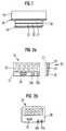
- FIG. 1 shows a composite of main carrier film 10 and display 20.
- the main carrier film 10 can be a tape 100 or a sheet 200 (FIGS. 3 and 4) on which the displays are manufactured.
- the main carrier film 10 must be stable and be resilient to the requirements of display manufacturing to be enough.
- a pressure-sensitive adhesive layer 30 is first applied to the main carrier film 10, and the carrier layer 21 is fixed on this pressure-sensitive adhesive layer 30.
- a functional layer 22 is generated, which forms the active layer of the display 20 and therefore also occasionally subsequently is referred to as display 22.
- the functional layer 22 can be processed such as evaporation, sputtering, spin coating, etc. are generated and for example a liquid crystal material, luminous materials or the like.
- the functional layer 22 can also have a plurality of layers and electrodes, Filters, polarizers, spacers etc. included.
- a base layer 23 with an integration adhesive layer 40 which for later fixation of the display 20 determined in or on a card body is arranged.
- the carrier layer 21 must be transparent.
- the displays 20 can also be reversed Order, d. H. starting with the base layer 23, and then transfer to the main carrier film by means of the pressure-sensitive adhesive layer 30 become.
- Another main carrier film can be used for this.
- the displays manufactured in this way must be turned over into integration into a chip card be, e.g. B. in that they are used for the manufacture
- Main carrier film are transferred to the main carrier film 10 in such a way as below in connection with the transfer of the displays to chip cards described.
- a pressure-sensitive adhesive is chosen that hardly Absorbs shear forces.
- the pressure-sensitive adhesive layer 30 are adhesives with good adhesion properties but only suitable for low cohesion properties.
- Adhesives in particular do not create a rigid bond between the bonded ones Materials, which is why moving parallel to the adhesive surface in a small amount Scope is possible while vertical removal from the adhesive surface high effort is necessary.
- Main carrier film a wound film tape 100 is used (Fig. 3). Because the use of the special adhesive 30 does not make it more solid Composite between the main carrier film 10 and carrier layer 21 is generated, so that the elongation of the surface of the wound main carrier film 100 is not from the pressure-sensitive adhesive layer is transferred to the carrier layer 21.
- This has to Consequence that the stresses caused by the winding in the functional layer 22 depend solely on the stretching of the surface of the carrier layer 21. Since the carrier layer 21 is extremely thin, this stretch is almost negligible.
- the integration adhesive layer 40 can also be used for the later integration of the displays in chip cards be exploited. Because smart cards often bend and other mechanically Exposed to loads, it is also advantageous for the integration adhesive layer 40 to use an adhesive that hardly absorbs shear forces. However, it is also possible to use a crosslinking adhesive, that is, an adhesive that also has good cohesive properties. The load the displays due to shear forces are additionally reduced by that the displays only have a very small thickness because of the carrier layer 21 and base layer 23 can be made very thin. The between the carrier layer 21 and the base layer 23, sensitive Functional layer 22 is therefore less stressed, since those which occur during bending Shear forces are lower in thin layers.
- the carrier and base layers 21, 23 preferably consist of PET and have Thicknesses of about 200 ⁇ m. But are z. B. phosphors in the functional layer 22 used to respond to environmental influences, can also be a layer of glass 21 can be used. Layer 23 must be rigid in this case, e.g. B. from Metal, to prevent breakage of the glass layer 21. Becomes the glass layer 21 additionally connected with a plastic film, another Increased resistance to breakage can be achieved. From a manufacturing point of view It can be seen with a combination of glass / metal for the carrier layer 21 and base layer 23 may be useful, as described above, the functional layer to apply to the base layer 23 (metal) and this by means of Cover glass layer 21 (carrier layer). For installation in a chip card then the described change to a second main carrier film is necessary.
- FIG. 2a shows a display 20 consisting of carrier layer 21, functional layer or display 22 and base layer 23 in plan view and in cross section. Those components 25 , 26a, 26b that are necessary for controlling the display are integrated in the functional layer 22. For this purpose, a display controller 25 and contact areas 26a, 26b are integrated on the carrier layer 21.
- the display 20 can be electrically conductively connected to the chip of a chip card via the contact surfaces 26a, 26b.
- FIG. 2b shows an alternative embodiment of that described with reference to FIG. 2a Displays 20 shown. The difference is that on a separate substrate 28, a prefabricated display 20 and the display controller 25 and the contact surfaces 26a, 26b are applied, which are connected to the display 20 be electrically connected.
- Both the compact display according to Figure 2a and the display module according to Figure 2b can be inserted into a chip card.
- the embodiment according to FIG. 2a it is preferred since finer conductive structures on the carrier layer 21 can be achieved and a separate electrical contact z.
- B. of Display controller 25 with the display 22 compared to the embodiment can be saved according to Figure 2b.
- the embodiment is after Figure 2a classify as particularly space-saving and inexpensive. In both cases it can be provided that the carrier film 21 only in the area of the actual Display, shown as a segment character in the figures 2a, b transparent is.
- FIG. 3 shows the transfer of the displays 20 from the main carrier film 10 a chip card 1 is shown.
- the main carrier film 10 forms with the displays 20 a transfer belt 100.
- Main carrier film 10 and displays 20 can also be designed as a multi-use sheet 200, as shown in Figure 4. this has the manner in which the displays 20 are transferred to the chip cards 1 no influence.
- the transfer belt 100 on a supply roll 50a is rolled up and unwound from it and wound onto the winding roll 50b becomes.
- the supply roll 50a on the take-up roll 50b is preferably carried out intermittently and synchronized with the provision of a chip card 1 which a display 20 is to be transmitted.
- the chip card 1 can also be a semi-finished product be, for example, a card insert, and only later to a finished one Card to be processed.
- the main carrier film 10 is shown in FIG. 3 as a transparent plastic band, so that the displays 20 can be seen through the main carrier film 10.
- the Embossing stamp 60 becomes a display 20 exactly on one under the transfer belt 100 positioned chip card 1 transferred in the hot stamping process, d. H. Smart card 1 and display 20 are connected by means of heat and pressure by a contact between the integration adhesive layer by means of the stamp 60 40 on the back of the display 20 and the surface of the chip card 1 will be produced.
- a cold gluing process can also be used be used in which, for. B. crosslinking liquid glue or Pressure sensitive adhesives are used.
- the adhesive forces of the pressure-sensitive adhesive layer 30 are so low compared to the adhesive forces of the integration adhesive layer 40 that the backing layer 21 of the display 20 is completely separated from the pressure-sensitive adhesive layer 30 triggers.
- the carrier layer 21 is thus after the transfer of the transfer belt 100 onto the chip card 1 as the outermost layer. It is as very thin optical layer formed so that the functional layer or Display 22 through the carrier layer 21 can be seen. After done Transfer, the transfer belt 100 is clocked further and a new chip card 1 so arranged under the transfer belt 100 that the transfer of next displays 20 can take place on the new chip card 1.
- the transfer of the display 20 to the chip card 1 can also be done according to the so-called Labeling technology take place, the displays 20 with a Glue attached to a carrier from which they can later be peeled off, because the adhesive sticks less well to the carrier than to the chip card 1 which is provided for the displays 20.
- a carrier z. B. siliconized Paper. That is, the displays arranged on the main carrier film 10 are applied to the chip card 1 with your integration adhesive layer 40, and the main carrier film 10 is then peeled off. This technique is particularly suitable in connection with that shown in Figure 4 Multi-purpose sheet 200.
- FIG. 20 A special embodiment of the invention is shown in FIG which the display 20 is transferred to a substrate 28, which is printed Printed circuit board is formed.
- the substrate 28 is intended as an insert for a card and therefore has at least the outer dimensions of a chip card 1.
- the dimensions of a chip card 1 are shown in dashed lines in FIG.
- the substrate 28 is also a chip 4 for the contacted Data transmission, a switch 3 and a battery 2 arranged and electrically connected to each other via cables.
- the display 20 corresponds the compact display shown in Figure 2a. But it is also possible instead of the compact display, a display module, as shown in Figure 2b, to use.
- the substrate 28 can be formed by the carrier layer 21 are, the electrical components 2, 3, 4 preferably first after the production of the display 20 is applied to the carrier layer 21 and be electrically connected to the display 20.
- the chip card can have a cover layer, for example one Foil to be coated, at least in the area of the display 22, as in Fig. 2a, b represented by segment characters is transparent. It can also be provided that a cover layer is used in the area of the display 22 has a recess if the carrier layer 21 is transparent is as described above, and has sufficient mechanical stability disposes.
- a base layer 23 can be dispensed with.
- the integration adhesive layer 40 is then directly to the ad, d. H. the functional layer 22, for example Can be produced by printing.
Landscapes
- Engineering & Computer Science (AREA)
- Computer Hardware Design (AREA)
- Microelectronics & Electronic Packaging (AREA)
- Physics & Mathematics (AREA)
- General Physics & Mathematics (AREA)
- Theoretical Computer Science (AREA)
- Credit Cards Or The Like (AREA)
Applications Claiming Priority (2)
| Application Number | Priority Date | Filing Date | Title |
|---|---|---|---|
| DE19923138A DE19923138C1 (de) | 1999-05-20 | 1999-05-20 | Display zur Integration in kartenförmige Trägermedien |
| DE19923138 | 1999-05-20 |
Publications (3)
| Publication Number | Publication Date |
|---|---|
| EP1054344A2 true EP1054344A2 (fr) | 2000-11-22 |
| EP1054344A3 EP1054344A3 (fr) | 2002-04-03 |
| EP1054344B1 EP1054344B1 (fr) | 2009-12-23 |
Family
ID=7908616
Family Applications (1)
| Application Number | Title | Priority Date | Filing Date |
|---|---|---|---|
| EP00110250A Expired - Lifetime EP1054344B1 (fr) | 1999-05-20 | 2000-05-19 | Afficheur pour intégration dans un support en forme de carte |
Country Status (3)
| Country | Link |
|---|---|
| EP (1) | EP1054344B1 (fr) |
| AT (1) | ATE453170T1 (fr) |
| DE (2) | DE19923138C1 (fr) |
Cited By (1)
| Publication number | Priority date | Publication date | Assignee | Title |
|---|---|---|---|---|
| FR2826315A1 (fr) * | 2001-06-22 | 2002-12-27 | Giesecke & Devrient Gmbh | Support de donnees avec element d'affichage |
Families Citing this family (16)
| Publication number | Priority date | Publication date | Assignee | Title |
|---|---|---|---|---|
| DE10065748A1 (de) * | 2000-12-29 | 2002-07-18 | Infineon Technologies Ag | Datenträgeranordnung mit einer Anzeigeeinrichtung |
| DE10119944A1 (de) * | 2001-04-24 | 2002-10-31 | Giesecke & Devrient Gmbh | Datenträgerkarte |
| DE10120254A1 (de) | 2001-04-25 | 2002-11-07 | Infineon Technologies Ag | Chipkartenmodul |
| DE10132893B4 (de) * | 2001-07-06 | 2014-02-27 | Giesecke & Devrient Gmbh | Verfahren zum Einbau eines Displayelements |
| DE10210606A1 (de) * | 2002-03-11 | 2003-10-09 | Giesecke & Devrient Gmbh | Tragbarer Datenträger mit Displaymodul und Verfahren zu seiner Herstellung |
| DE10210608C1 (de) * | 2002-03-11 | 2003-10-09 | Giesecke & Devrient Gmbh | Tragbarer Datenträger mit Display und Verfahren zu seiner Herstellung |
| DE10215398B4 (de) * | 2002-04-08 | 2005-12-15 | Giesecke & Devrient Gmbh | Tragbarer Datenträger mit Display |
| DE10239564A1 (de) * | 2002-08-28 | 2005-03-17 | Giesecke & Devrient Gmbh | Tragbarer Datenträger mit Anzeigevorrichtung |
| DE10308477A1 (de) * | 2002-09-30 | 2004-04-08 | Orga Kartensysteme Gmbh | Chipkarte |
| DE10248386B4 (de) * | 2002-10-17 | 2006-08-31 | Giesecke & Devrient Gmbh | Tragbarer elektronischer Datenträger mit integriertem Display |
| DE10248394A1 (de) * | 2002-10-17 | 2004-05-13 | Giesecke & Devrient Gmbh | Tragbarer elektronischer Datenträger |
| NL1024323C2 (nl) * | 2003-09-18 | 2005-03-21 | Tno | Identificatiekaart. |
| US7821794B2 (en) | 2005-04-11 | 2010-10-26 | Aveso, Inc. | Layered label structure with timer |
| US7599192B2 (en) * | 2005-04-11 | 2009-10-06 | Aveso, Inc. | Layered structure with printed elements |
| DE102007017133A1 (de) * | 2007-04-11 | 2008-10-16 | Giesecke & Devrient Gmbh | Verfahren zum Herstellen eines kartenförmigen Datenträgers und kartenförmiger Datenträger |
| DE102009016527A1 (de) * | 2009-04-06 | 2010-10-07 | Giesecke & Devrient Gmbh | Verfahren und Vorrichtung zum sicheren Eingeben eines Zugangscodes für einen sicheren Zugang zu einem elektronischen Dienst |
Family Cites Families (5)
| Publication number | Priority date | Publication date | Assignee | Title |
|---|---|---|---|---|
| JP3081122B2 (ja) * | 1994-07-18 | 2000-08-28 | シャープ株式会社 | 基板搬送用治具及びそれを用いた液晶表示素子の製造方法 |
| DE19631557A1 (de) * | 1996-07-29 | 1998-02-05 | Kuban Waldemar | Anzeigedisplay für die Chipkarte |
| DE19649761C2 (de) * | 1996-11-30 | 2003-04-03 | Univ Stuttgart | Verfahren zur Herstellung von Flüssigkristall-Displays auf Kunststoff-Folien unter Verwendung von bistabilen Flüssigkristallen |
| SE9701612D0 (sv) * | 1997-04-29 | 1997-04-29 | Johan Asplund | Smartcard and method for its manufacture |
| DE19732161A1 (de) * | 1997-07-25 | 1999-01-28 | Hoechst Ag | Chipkarte mit mechanisch belastbarer bistabiler Anzeige |
-
1999
- 1999-05-20 DE DE19923138A patent/DE19923138C1/de not_active Expired - Fee Related
-
2000
- 2000-05-19 EP EP00110250A patent/EP1054344B1/fr not_active Expired - Lifetime
- 2000-05-19 DE DE50015826T patent/DE50015826D1/de not_active Expired - Lifetime
- 2000-05-19 AT AT00110250T patent/ATE453170T1/de not_active IP Right Cessation
Cited By (1)
| Publication number | Priority date | Publication date | Assignee | Title |
|---|---|---|---|---|
| FR2826315A1 (fr) * | 2001-06-22 | 2002-12-27 | Giesecke & Devrient Gmbh | Support de donnees avec element d'affichage |
Also Published As
| Publication number | Publication date |
|---|---|
| DE50015826D1 (de) | 2010-02-04 |
| EP1054344A3 (fr) | 2002-04-03 |
| ATE453170T1 (de) | 2010-01-15 |
| DE19923138C1 (de) | 2000-11-02 |
| EP1054344B1 (fr) | 2009-12-23 |
Similar Documents
| Publication | Publication Date | Title |
|---|---|---|
| EP1054344B1 (fr) | Afficheur pour intégration dans un support en forme de carte | |
| EP2197686B1 (fr) | Élément de sécurité pour caractériser un document de sécurité et procédé pour produire cet élément de sécurité | |
| EP1940618B1 (fr) | Procede de transfert d'un corps multicouche et feuille de transfert | |
| DE69806515T2 (de) | Elektronische vorrichtung mit wegwerfchip und verfahren zu deren herstellung | |
| EP2150924B1 (fr) | Procédé de réalisation d'une antenne auto-collante pour système RFID | |
| DE69929981T2 (de) | Verfahren zum herstellen einer kontaktlosen chipkarte | |
| DE69609425T2 (de) | Notizblock gebildet aus blättern die mit koadhesivem selbstklebestoff zusammen verbunden sind | |
| WO2005076206A1 (fr) | Procede et dispositif pour produire en continu des composants electroniques a couche mince, et composant electronique a couche mince | |
| EP0733490B1 (fr) | Formulaire avec carte intégrée et séparable et matérial multicouche pour sa fabrication | |
| DE102017100302A1 (de) | Flüssigkristallanzeigefeld | |
| EP4143445A1 (fr) | Système de fixation | |
| EP2821218B9 (fr) | Procédé de fabrication d'un étiquette adhésive composite imprimée | |
| EP2285586B1 (fr) | Support d'impression composé d'au moins deux supports d'impression partiels assemblés de façon coplanaire, supports d'impression partiels et procédé de fabrication de ceux-ci | |
| EP1948450B1 (fr) | Procédé pour réaliser un support de données sous forme de carte comportant une zone d'inscription | |
| EP1089220B1 (fr) | Bande multicouches de matériau laminé comprenant des transpondeurs RF-ID, en particulier en rouleau | |
| EP1168239A2 (fr) | Etiquette adhésive | |
| EP3701423A1 (fr) | Étiquette de sécurité permettant de déceler une tentative de manipulation frauduleuse | |
| EP3008668B1 (fr) | Procédé de fabrication pour des supports de données portatifs | |
| WO1999008256A1 (fr) | Materiaux multicouches et leurs utilisations | |
| DE10010652B4 (de) | Selbstklebende Tapete, insbesondere Tapetenborte, und Verfahren zu ihrer Herstellung | |
| WO2020114620A2 (fr) | Application et fixation d'un nombre défini d'éléments individuels sur une bande de substrat | |
| EP2599037B1 (fr) | Ensemble transpondeur flexible | |
| EP0803379A1 (fr) | Carte banquaire, formulaire avec carte banquaire intégrale et la méthode pour sa fabrication | |
| EP0737955A1 (fr) | Etiquette auto-collante | |
| DE29924410U1 (de) | Selbstklebendes Schild |
Legal Events
| Date | Code | Title | Description |
|---|---|---|---|
| PUAI | Public reference made under article 153(3) epc to a published international application that has entered the european phase |
Free format text: ORIGINAL CODE: 0009012 |
|
| 17P | Request for examination filed |
Effective date: 20000519 |
|
| AK | Designated contracting states |
Kind code of ref document: A2 Designated state(s): AT BE CH CY DE DK ES FI FR GB GR IE IT LI LU MC NL PT SE |
|
| AX | Request for extension of the european patent |
Free format text: AL;LT;LV;MK;RO;SI |
|
| PUAL | Search report despatched |
Free format text: ORIGINAL CODE: 0009013 |
|
| AK | Designated contracting states |
Kind code of ref document: A3 Designated state(s): AT BE CH CY DE DK ES FI FR GB GR IE IT LI LU MC NL PT SE |
|
| AX | Request for extension of the european patent |
Free format text: AL;LT;LV;MK;RO;SI |
|
| RIC1 | Information provided on ipc code assigned before grant |
Free format text: 7G 06K 19/07 A, 7G 06K 19/077 B, 7G 02F 1/1333 B |
|
| AKX | Designation fees paid |
Free format text: AT BE CH CY DE DK ES FI FR GB GR IE IT LI LU MC NL PT SE |
|
| 17Q | First examination report despatched |
Effective date: 20061208 |
|
| 17Q | First examination report despatched |
Effective date: 20061208 |
|
| GRAP | Despatch of communication of intention to grant a patent |
Free format text: ORIGINAL CODE: EPIDOSNIGR1 |
|
| GRAS | Grant fee paid |
Free format text: ORIGINAL CODE: EPIDOSNIGR3 |
|
| GRAA | (expected) grant |
Free format text: ORIGINAL CODE: 0009210 |
|
| AK | Designated contracting states |
Kind code of ref document: B1 Designated state(s): AT BE CH CY DE DK ES FI FR GB GR IE IT LI LU MC NL PT SE |
|
| REG | Reference to a national code |
Ref country code: GB Ref legal event code: FG4D Free format text: NOT ENGLISH |
|
| REG | Reference to a national code |
Ref country code: CH Ref legal event code: EP |
|
| REG | Reference to a national code |
Ref country code: IE Ref legal event code: FG4D |
|
| REF | Corresponds to: |
Ref document number: 50015826 Country of ref document: DE Date of ref document: 20100204 Kind code of ref document: P |
|
| REG | Reference to a national code |
Ref country code: NL Ref legal event code: VDEP Effective date: 20091223 |
|
| PG25 | Lapsed in a contracting state [announced via postgrant information from national office to epo] |
Ref country code: FI Free format text: LAPSE BECAUSE OF FAILURE TO SUBMIT A TRANSLATION OF THE DESCRIPTION OR TO PAY THE FEE WITHIN THE PRESCRIBED TIME-LIMIT Effective date: 20091223 Ref country code: SE Free format text: LAPSE BECAUSE OF FAILURE TO SUBMIT A TRANSLATION OF THE DESCRIPTION OR TO PAY THE FEE WITHIN THE PRESCRIBED TIME-LIMIT Effective date: 20091223 |
|
| REG | Reference to a national code |
Ref country code: IE Ref legal event code: FD4D |
|
| PG25 | Lapsed in a contracting state [announced via postgrant information from national office to epo] |
Ref country code: NL Free format text: LAPSE BECAUSE OF FAILURE TO SUBMIT A TRANSLATION OF THE DESCRIPTION OR TO PAY THE FEE WITHIN THE PRESCRIBED TIME-LIMIT Effective date: 20091223 Ref country code: PT Free format text: LAPSE BECAUSE OF FAILURE TO SUBMIT A TRANSLATION OF THE DESCRIPTION OR TO PAY THE FEE WITHIN THE PRESCRIBED TIME-LIMIT Effective date: 20100423 Ref country code: ES Free format text: LAPSE BECAUSE OF FAILURE TO SUBMIT A TRANSLATION OF THE DESCRIPTION OR TO PAY THE FEE WITHIN THE PRESCRIBED TIME-LIMIT Effective date: 20100403 |
|
| PG25 | Lapsed in a contracting state [announced via postgrant information from national office to epo] |
Ref country code: IE Free format text: LAPSE BECAUSE OF FAILURE TO SUBMIT A TRANSLATION OF THE DESCRIPTION OR TO PAY THE FEE WITHIN THE PRESCRIBED TIME-LIMIT Effective date: 20091223 Ref country code: CY Free format text: LAPSE BECAUSE OF FAILURE TO SUBMIT A TRANSLATION OF THE DESCRIPTION OR TO PAY THE FEE WITHIN THE PRESCRIBED TIME-LIMIT Effective date: 20091223 Ref country code: GR Free format text: LAPSE BECAUSE OF FAILURE TO SUBMIT A TRANSLATION OF THE DESCRIPTION OR TO PAY THE FEE WITHIN THE PRESCRIBED TIME-LIMIT Effective date: 20100324 |
|
| PLBE | No opposition filed within time limit |
Free format text: ORIGINAL CODE: 0009261 |
|
| STAA | Information on the status of an ep patent application or granted ep patent |
Free format text: STATUS: NO OPPOSITION FILED WITHIN TIME LIMIT |
|
| BERE | Be: lapsed |
Owner name: GIESECKE & DEVRIENT G.M.B.H. Effective date: 20100531 |
|
| 26N | No opposition filed |
Effective date: 20100924 |
|
| PG25 | Lapsed in a contracting state [announced via postgrant information from national office to epo] |
Ref country code: MC Free format text: LAPSE BECAUSE OF NON-PAYMENT OF DUE FEES Effective date: 20100531 |
|
| REG | Reference to a national code |
Ref country code: CH Ref legal event code: PL |
|
| PG25 | Lapsed in a contracting state [announced via postgrant information from national office to epo] |
Ref country code: DK Free format text: LAPSE BECAUSE OF FAILURE TO SUBMIT A TRANSLATION OF THE DESCRIPTION OR TO PAY THE FEE WITHIN THE PRESCRIBED TIME-LIMIT Effective date: 20091223 |
|
| PG25 | Lapsed in a contracting state [announced via postgrant information from national office to epo] |
Ref country code: CH Free format text: LAPSE BECAUSE OF NON-PAYMENT OF DUE FEES Effective date: 20100531 Ref country code: LI Free format text: LAPSE BECAUSE OF NON-PAYMENT OF DUE FEES Effective date: 20100531 |
|
| PG25 | Lapsed in a contracting state [announced via postgrant information from national office to epo] |
Ref country code: BE Free format text: LAPSE BECAUSE OF NON-PAYMENT OF DUE FEES Effective date: 20100531 Ref country code: IT Free format text: LAPSE BECAUSE OF FAILURE TO SUBMIT A TRANSLATION OF THE DESCRIPTION OR TO PAY THE FEE WITHIN THE PRESCRIBED TIME-LIMIT Effective date: 20091223 |
|
| PG25 | Lapsed in a contracting state [announced via postgrant information from national office to epo] |
Ref country code: AT Free format text: LAPSE BECAUSE OF NON-PAYMENT OF DUE FEES Effective date: 20100519 |
|
| PG25 | Lapsed in a contracting state [announced via postgrant information from national office to epo] |
Ref country code: LU Free format text: LAPSE BECAUSE OF NON-PAYMENT OF DUE FEES Effective date: 20100519 |
|
| REG | Reference to a national code |
Ref country code: DE Ref legal event code: R082 Ref document number: 50015826 Country of ref document: DE |
|
| REG | Reference to a national code |
Ref country code: FR Ref legal event code: PLFP Year of fee payment: 17 |
|
| REG | Reference to a national code |
Ref country code: FR Ref legal event code: PLFP Year of fee payment: 18 |
|
| PGFP | Annual fee paid to national office [announced via postgrant information from national office to epo] |
Ref country code: DE Payment date: 20170531 Year of fee payment: 18 Ref country code: FR Payment date: 20170522 Year of fee payment: 18 Ref country code: GB Payment date: 20170524 Year of fee payment: 18 |
|
| REG | Reference to a national code |
Ref country code: DE Ref legal event code: R081 Ref document number: 50015826 Country of ref document: DE Owner name: GIESECKE+DEVRIENT MOBILE SECURITY GMBH, DE Free format text: FORMER OWNER: GIESECKE & DEVRIENT GMBH, 81677 MUENCHEN, DE |
|
| REG | Reference to a national code |
Ref country code: GB Ref legal event code: 732E Free format text: REGISTERED BETWEEN 20180118 AND 20180124 |
|
| REG | Reference to a national code |
Ref country code: FR Ref legal event code: TP Owner name: GIESECKE+DEVRIENT MOBILE SECURITY GMBH, DE Effective date: 20180619 |
|
| REG | Reference to a national code |
Ref country code: DE Ref legal event code: R119 Ref document number: 50015826 Country of ref document: DE |
|
| GBPC | Gb: european patent ceased through non-payment of renewal fee |
Effective date: 20180519 |
|
| PG25 | Lapsed in a contracting state [announced via postgrant information from national office to epo] |
Ref country code: GB Free format text: LAPSE BECAUSE OF NON-PAYMENT OF DUE FEES Effective date: 20180519 Ref country code: FR Free format text: LAPSE BECAUSE OF NON-PAYMENT OF DUE FEES Effective date: 20180531 Ref country code: DE Free format text: LAPSE BECAUSE OF NON-PAYMENT OF DUE FEES Effective date: 20181201 |