EP1054537A1 - Demodulateur numerique pour transmission hierarchisee - Google Patents
Demodulateur numerique pour transmission hierarchisee Download PDFInfo
- Publication number
- EP1054537A1 EP1054537A1 EP98955991A EP98955991A EP1054537A1 EP 1054537 A1 EP1054537 A1 EP 1054537A1 EP 98955991 A EP98955991 A EP 98955991A EP 98955991 A EP98955991 A EP 98955991A EP 1054537 A1 EP1054537 A1 EP 1054537A1
- Authority
- EP
- European Patent Office
- Prior art keywords
- carrier
- signal
- value
- output
- accordance
- Prior art date
- Legal status (The legal status is an assumption and is not a legal conclusion. Google has not performed a legal analysis and makes no representation as to the accuracy of the status listed.)
- Granted
Links
- 230000005540 biological transmission Effects 0.000 title claims abstract description 61
- 238000010586 diagram Methods 0.000 description 13
- 238000001514 detection method Methods 0.000 description 10
- 230000001186 cumulative effect Effects 0.000 description 5
- 238000000034 method Methods 0.000 description 5
- 239000006185 dispersion Substances 0.000 description 3
- 238000001914 filtration Methods 0.000 description 3
- 230000010355 oscillation Effects 0.000 description 2
- 239000000969 carrier Substances 0.000 description 1
- 238000002474 experimental method Methods 0.000 description 1
- 238000005259 measurement Methods 0.000 description 1
- 239000000725 suspension Substances 0.000 description 1
Images





Classifications
-
- H—ELECTRICITY
- H04—ELECTRIC COMMUNICATION TECHNIQUE
- H04L—TRANSMISSION OF DIGITAL INFORMATION, e.g. TELEGRAPHIC COMMUNICATION
- H04L27/00—Modulated-carrier systems
- H04L27/18—Phase-modulated carrier systems, i.e. using phase-shift keying
- H04L27/22—Demodulator circuits; Receiver circuits
- H04L27/233—Demodulator circuits; Receiver circuits using non-coherent demodulation
- H04L27/2332—Demodulator circuits; Receiver circuits using non-coherent demodulation using a non-coherent carrier
-
- H—ELECTRICITY
- H04—ELECTRIC COMMUNICATION TECHNIQUE
- H04L—TRANSMISSION OF DIGITAL INFORMATION, e.g. TELEGRAPHIC COMMUNICATION
- H04L27/00—Modulated-carrier systems
- H04L27/0014—Carrier regulation
- H04L2027/0024—Carrier regulation at the receiver end
- H04L2027/0026—Correction of carrier offset
- H04L2027/003—Correction of carrier offset at baseband only
-
- H—ELECTRICITY
- H04—ELECTRIC COMMUNICATION TECHNIQUE
- H04L—TRANSMISSION OF DIGITAL INFORMATION, e.g. TELEGRAPHIC COMMUNICATION
- H04L27/00—Modulated-carrier systems
- H04L27/0014—Carrier regulation
- H04L2027/0044—Control loops for carrier regulation
- H04L2027/0053—Closed loops
- H04L2027/0057—Closed loops quadrature phase
-
- H—ELECTRICITY
- H04—ELECTRIC COMMUNICATION TECHNIQUE
- H04L—TRANSMISSION OF DIGITAL INFORMATION, e.g. TELEGRAPHIC COMMUNICATION
- H04L27/00—Modulated-carrier systems
- H04L27/0014—Carrier regulation
- H04L2027/0044—Control loops for carrier regulation
- H04L2027/0071—Control of loops
- H04L2027/0079—Switching between loops
- H04L2027/0081—Switching between loops between loops of different bandwidths
-
- H—ELECTRICITY
- H04—ELECTRIC COMMUNICATION TECHNIQUE
- H04L—TRANSMISSION OF DIGITAL INFORMATION, e.g. TELEGRAPHIC COMMUNICATION
- H04L27/00—Modulated-carrier systems
- H04L27/0014—Carrier regulation
- H04L2027/0083—Signalling arrangements
- H04L2027/0089—In-band signals
- H04L2027/0093—Intermittant signals
- H04L2027/0095—Intermittant signals in a preamble or similar structure
Definitions
- the present invention relates to a hierarchical transmission digital demodulator for demodulating digital modulated waves multiplexed on a time axis by a plurality of modulation methods in which necessary C/N (ratio of carrier power to noise power) values are different.
- a hierarchical transmission method is known by which digital modulated waves multiplexed on a time axis by a plurality of modulation methods in which necessary C/N values, e.g., 8PSK modulation waves, QPSk modulation waves and BPSK modulation waves, are combined to form frames which are repetitively transmitted.
- C/N values e.g. 8PSK modulation waves, QPSk modulation waves and BPSK modulation waves
- BPSK modulation waves including burst symbol signals
- the sync capture is obtained by receiving the BPSK modulation waves (including burst symbol signals) and after the sync capture is obtained, sequentially input BPSK modulation signals, burst symbol signals (BPSK modulation signals), QPSK modulation signals and 8PSK modulation signals are demodulated (continuously demodulated) in the order of input signals.
- the reception C/N value is degraded during the continuous demodulation, the reception state of 8PSK modulation waves requiring a high necessary C/N value is degraded. Therefore, at the receivable limit C/N value of lower hierarchical QPSK or BPSK modulation waves, a carrier slip occurs in the section of 8PSK modulation waves and the frame sync of the system cannot be captured. The necessary C/N value is therefore substantially raised and the reception state becomes unstable.
- a hierarchical transmission demodulator of this invention comprises: first carrier reproducing means for reproducing a carrier in accordance with demodulation outputs that a modulated wave in a header section and a modulated wave of a burst symbol signal are demodulated means for measuring a reception C/N value; second carrier reproducing means for reproducing the carrier in accordance with continuous demodulation outputs if the measured reception C/N value after the sync capture is equal to or larger than a first predetermined threshold; third carrier reproducing means for reproducing the carrier in accordance with demodulation outputs for a hierarchical level except a high hierarchical level if the measured reception C/N value which is equal to or larger than a second threshold which is lower than the first threshold.
- the carrier is reproduced by the first carrier reproducing means in accordance with demodulation outputs that a modulated wave in a header section and a modulated wave of a burst symbol signal are demodulated. Accordingly, the carrier can be reproduced reliably.
- a reception C/N value is measured by the C/N measuring means and if the reception C/N value after the sync capture is equal to or larger than the first predetermined threshold after the sync capture, the carrier is reproduced by the second carrier reproducing means in accordance with the continuous demodulation output. It is therefore possible to prevent jitters, etc. to be caused by inability of following a frequency change while the carrier is not reproduced.
- the carrier is reproduced by the third carrier reproducing means in accordance with demodulation outputs for a hierarchical level except a high hierarchical level.
- the hierarchical transmission digital demodulator of this invention further comprises reproduction loop characteristic switching means for switching a carrier reproduction to a different carrier reproduction characteristic during carrier reproduction by the first carrier reproducing means and during carrier reproduction by the carrier reproducing means different from the first carrier reproducing means.
- the reproduction loop characteristic is switched between different carrier reproduction characteristics during carrier reproduction by the first carrier reproducing means and during carrier reproduction by the carrier reproducing means different from the first carrier reproducing means.
- Fig. 1 is a block diagram showing the structure of a hierarchical transmission digital demodulator according to an embodiment of the invention.
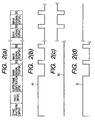
- FIG. 2(a) is a diagram showing an example of the frame structure used by the hierarchical transmission system.
- One frame is constituted of one header of 192 symbols and a plurality of pairs of 203 symbols and 4 symbols, totalling in 39936 symbols.
- one frame is constituted of: a frame sync pattern (BPSK) of 32 symbols; a transmission and multiplexing configuration control pattern (TMCC) (BPSK) of 128 symbols for transmission and multiplexing configuration identification; a super-frame identification information pattern of 32 symbols; a main signal (TC8PSK) of 203 symbols and a burst symbol signal (BPSK) of 4 symbols (indicated by BS in Fig.
- 8 frames are called a super-frame and the super-frame identification information pattern is used for identifying the super-frame.
- 192 symbols from the frame sync pattern to the end of the super-frame identification information pattern is also called the header.
- the hierarchical transmission digital demodulator has an arithmetic circuit 1, a numerical control oscillator 2, a roll-off filer 3 composed of a digital filter having the raised cosine characteristics, a frame sync timing circuit 4, a transmission mode judging circuit 5, a carrier reproduction phase error detection circuit 6, a carrier filer 7 composed of a low-pass digital filter, a gain control circuit 8, an automatic frequency control (AFC) circuit 9, a CNR measuring circuit 10 and a logical gate circuit 11.
- AFC automatic frequency control
- the AFC circuit 9 has a cumulative adder 91 and a latch circuit 92 which latches an output of the cumulative adder 91 and outputs it to the cumulative adder 91.
- the numerical control oscillator 2 has a sine table 23 for receiving a latch output from the latch circuit 92 to output sine data 23a and 23b of opposite polarities and a cosine table 24 for receiving the latch output from the latch circuit 92 to output cosine data 24a and 24b.
- the numerical control oscillator 2 outputs the sine data 23a and 23b and cosine data 24a and 24b of opposite polarities, to output sine and cosine signals of opposite polarities which substantially form a reproduction carrier in cooperation with the AFC circuit 9.
- the arithmetic circuit has, as shown in Fig. 3,: a multiplier 1a for multiplying a quasi-sync detected I axis baseband signal i by the sine data 23a; a multiplier 1b for multiplying the baseband signal i by the cosine data 24a; a multiplier 1d for multiplying a quasi-sync detected Q axis baseband signal q by the opposite polarity sine data 23b; a multiplier 1e for multiplying the baseband signal q by the cosine data 24b; an adder 1c for adding outputs of the multipliers 1b and 1d to output the addition result as a baseband signal I, and an adder 1f for adding outputs of the multipliers 1a and 1e to output the addition result as a baseband signal Q.
- the arithmetic circuit 1 therefore tunes the frequencies of the baseband signals i and q and outputs the frequency tuned baseband signals I and Q to the roll-off filter 3.
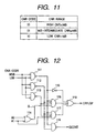
- the frame sync timing circuit 4 Upon reception of baseband signals ID and QD output from the roll-off filter 3, the frame sync timing circuit 4 outputs a TMCC pattern to the transmission mode judging circuit 5. In accordance with the decoded result of the TMCC pattern, the transmission mode judging circuit 5 supplies the frame sync timing circuit 4 with a 2-bit transmission mode signal shown in Fig.
- an 8PSK signal which is a high hierarchical signal (demodulation output that the 8PSK modulated signal is demodulated is referred to as an 8PSK signal); a QFSK signal which is a low hierarchical (demodulation output that the QPSK modulated signal is demodulated is referred to as a QPSK signal); the 8PSK signal and QPSK signal; and the 8PSK signal and BPSK signal (demodulation output that the BPSK modulated signal is demodulated is referred to as a BPSK signal).
- the transmission mode signal takes a value "00" for the 8PSK signal, a value "01” for the QPSK signal, a value “10” for the 8PSK signal and QPSK signal, and a value "11” for The 8PSK signal and BPSK signal.
- the frame sync timing circuit 4 receives the baseband signals ID and QD to detect a sync pattern and output a frame sync signal FSYNC, and also receives the transmission mode signal to output a signal AI shown in Fig. 2(b) which takes a high level during the header section and burst symbol signal section, and a signal AO shown in Fig. 2(c) which takes a high level during the QPSK signal section.
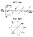
- the carrier reproduction phase error detection circuit 6 receives The baseband signals ID and QD and signals AI and AO to detect a phase error and output a phase error voltage corresponding to the detected phase error. More specifically, the carrier reproduction phase error detection circuit 6 is provided with a phase error table for the BPSK signal shown in Figs. 7(a) and (b), a phase error table for the QPSK signal shown in Figs. 8(a) and 8(b), and a phase error table for the 8PSK signal shown in Figs. 9(a) and 9(b).
- the carrier reproduction phase error detection circuit 6 judges the transmission mode in accordance with the signals AI and AO, selects the phase error table in accordance with the judged transmission mode, obtains the phase from the signal point arrangement of the baseband signals ID and QD, and outputs a phase error voltage corresponding to the phase.
- the carrier reproduction phase error detection circuit 6 selects the phase error table shown in Figs. 7(a) and 7(b), and outputs: a negative phase error voltage shown in Fig. 7(a) for the phase in an increase direction in the range from the phase equal to or larger than 3 ⁇ /2 radian to the phase smaller than 0 (2 ⁇ ) radian; a positive phase error voltage shown in Fig.
- phase error voltage takes the maximum value in the increase direction (+) at 3 ⁇ /2 radian and the maximum value in the decrease direction (-) at ⁇ /2 radian.
- the carrier reproduction phase error detection circuit 6 selects the phase error table shown in Figs. 8(a) and 8(b).
- the phase error voltage takes the + direction maximum value or - direction maximum value at the phase of 0 (2 ⁇ ) radian, ⁇ /2 radian, ⁇ radian or 3 ⁇ /4 radian, the maximum value being a half of that of the BPSK signal.
- the carrier reproduction phase error detection circuit 6 selects the phase error table shown in Figs. 9(a) and 9(b).
- the phase error voltage takes the + direction maximum value or - direction maximum value at the phase of ⁇ /8 radian, 3 ⁇ /8 radian, 5 ⁇ /8 radian, 7 ⁇ /8 radian, 9 ⁇ /8 radian, 11 ⁇ /8 radian, 13 ⁇ /8 radian, or 15 ⁇ /8 radian, the maximum value being a quarter of that of the BPSK signal.
- the description for the phase error voltage to be output when the transmission mode corresponds to the 8PSK signal is omitted, since this can be easily understood from the description for the transmission mode for the BPSK signal.
- the phase error voltage output from the carrier reproduction phase error detection circuit 6 is supplied to the carrier filter 7 composed of a digital low-pass filter to smooth the phase error voltage.
- the filtering operation is selectively executed in accordance with a CNR code output from the logical gate circuit 11 to be described later and with a carrier filter control signal (CRFLGP) suitable for the mode identified by the signals AI and AO.
- CRFLGP carrier filter control signal
- An output of the carrier filter 7 is supplied to the gain control circuit 8 which controls the gain in accordance with a gain control signal (GCONT) output from the logical gate circuit 11 for each of a high C/N value and an intermediate C/N value.
- GCONT gain control signal
- the output is supplied to the cumulative adder 91 of the AFC circuit 9 to add the output to a voltage value of the AFC circuit 9 which determines a scanning step frequency, so that a change in the oscillation frequency of the numerical control oscillator 2 is made faster.
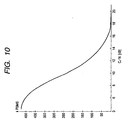
- the CNR measuring circuit 10 receives the baseband signals ID and QD, calculates a dispersion value of the signal point arrangement data obtained from the baseband signals ID and QD, compares the dispersion value with a predetermined threshold value, counts the number (DSMS) of occurrences of a dispersion value in excess of the threshold value per a predetermined unit time, and refers to a table shown in Fig. 10 formed through experiments by using the occurrence frequency (DSMS) as a search key to thereby obtain a C/N value which is output as a 2-bit CNR code. For example, as shown in Fig.
- the CNR code takes a value "00” at a high CNR equal to or larger than 9dB, a value "01” at an intermediate CNR equal to or larger than 4dB and smaller than 9dB, and a value "10” at a low CNR smaller than 4 dB.
- the logical gate circuit 11 receives the signals AI and AO output from the frame sync timing circuit 4 and the CNR code output from the CNR measuring circuit 10, and outputs the carrier filter control signal (CRFLGP) and gain control signal (GCONT).
- CRFLGP carrier filter control signal
- GCONT gain control signal
- the logical gate circuit 11 has: NAND gates 111, 112 and 113 for receiving the CNR code and outputting signals corresponding to the high, intermediate and low C/N values; an OR gate 114 for receiving the signals AI and AO and outputting a signal G such as shown in Fig.
- the logical gate circuit 11 outputs the high potential carrier filter control signal (CRFLGP) irrespective of the discriminated mode (in any section of the header, burst symbol signal, QPSK signal and 8PSK signal), at the intermediate C/N it outputs the high potential carrier filter control signal (CRFLGP) in any section of the header, burst symbol signal and QPSK signal, and at the low C/N it outputs the high potential carrier filter control signal (CRFLGP) in any section of the header and burst symbol signal. In other cases, the low potential carrier filter control signal (CRFLGP) is output.
- the logical gate circuit 11 also outputs the high potential gain control signal (GCONT) at the high or intermediate C/N, and the low potential gain control signal at the low C/N.
- the carrier filter 8 executes a filtering operation to smooth and output the phase error voltage.
- the carrier filter 8 stops the filtering operation so that the output immediately before the stop is held and output.
- the gain control circuit 8 amplifies the output of the carrier filter 7 two times and outputs it.
- the gain control circuit 8 outputs the output of the carrier filter 7 as it is.
- the baseband signals i and q are multiplied by the arithmetic circuit 1 by the orthogonal reproduction carriers output from the numerical control oscillator 2 so that the frequencies of the baseband signals i and q are tuned and the baseband signals are supplied as the baseband signals ID and QD to the frame sync timing circuit 4 via the roll-off filter 3.
- the frame sync timing circuit 4 supplies the TMCC pattern to the transmission mode judging circuit 5 which decodes the TMCC pattern to supply the transmission mode signal to the frame sync timing circuit 4.
- the frame sync timing circuit 4 Upon reception of the baseband signals ID and QD and transmission mode signal, the frame sync timing circuit 4 detects the frame sync pattern and outputs the frame sync signal SYNC and signals AI and AO.
- the frame sync signal SYNC is supplied to the gain control circuit 8 so that each time the frame sync is detected, the operation of the gain control circuit 8 is reset.
- the signals AI and AO are supplied to the carrier reproduction phase error detection circuit 6 and logical gate circuit 11.
- the carrier reproduction phase error detection circuit 6 selects a proper phase error table in accordance with the baseband signals and signals AI and AO to detect the phase error voltage which is supplied to the carrier filter 7 to be smoothed.
- the CNR measuring circuit 10 counts the number DSMS in accordance with the signal point arrangement of the baseband signals ID and QD. In accordance with the counted DSMS, the C/N value is obtained and output as the CNR code.
- the logical gate circuit 11 Upon reception of the CNR code and signals AI and AO, the logical gate circuit 11 checks whether the C/N value is the high, intermediate or low C/N value. If the CN value is either the high or intermediate C/N value, the gain control signal (GCONT) is supplied to the gain control circuit 8 to set a high loop gain of the gain control circuit 8 so that the phase error voltage output from the carrier filer 7 is amplified two times and output. If the logical gate circuit 11 judges the C/N value as the low C/N value, the gain control signal (GCONT) controls the gain control circuit 8 to take a low loop gain so that the phase error voltage output from the carrier filter 7 is output as it is.
- the gain control signal GCONT
- the cumulative adder 91 of the AFC circuit 9 Upon reception of an output from the gain control circuit 8, the cumulative adder 91 of the AFC circuit 9 cumulatively adds the output voltage of the gain control circuit 8 to the voltage value generated by the AFC circuit which voltage value determines the scanning step frequency. Therefore, the oscillation frequency of the numerical control oscillator 2 is changed so that the frequency scanning width is changed and then reproduction carrier frequency is changed.
- Step S1 As the power is turned on, the AFC circuit 9 scans the frequency to change the reproduction carrier frequency (Step S1), and this frequency scan at Step S1 continues until a frame sync pattern is detected (Step S2).
- Step S2 a burst demodulation mode starts demodulating the BPSK signal and burst symbol signal (Step S3). After Step S3, reception C/N is measured (Step S4).
- Step S5 After the reception C/N value is measured at Step S4, it is checked whether the frame sync signal FSYNC is detected a plurality of times in succession (Step S5). If the frame sync signal FSYNC is not detected a plurality of times in succession, it is judged that the frame sync is not established and the flow returns to Step S1 to repeat the above operations. If the frame sync signal FSYNC is detected a plurality of times in succession, after Step S5 the transmission mode is analyzed in accordance with a decode output of the TMCC pattern (Step S6).
- Step S6 it is checked whether the reception C/N value takes a high C/N value (Step S7). If it is judged at Step S7 that the reception C/N value takes the high C/N value, demodulation for each hierarchy or continuous demodulation is performed (Step S8). Next, the gain of the gain control circuit 8 is set to a high loop gain (Step S9) to thereafter return to Step S4 to repeat the above operations.
- a high potential signal output from the inverter 115 is output as the carrier filter control signal (CRFLGP) so that the carrier filter 7 is controlled to be in an operation state to sequentially demodulate the sections of the header, burst symbol signal, QPSK signal and 8PSK signal in this input order.
- the NAND gate 119 outputs a high potential signal as the gain control signal (GCONT) so that the gain control circuit is controlled to be in a high gain state.
- Step S10 If it is judged at Step S7 that the reception C/N value is not the high C/N value, it is then judged whether the reception C/N value is an intermediate C/N value or not (Step S10). If it is judged at Step S10 that the reception value is not the intermediate C/N value, the flow reruns to Step S2 to repeat the above operations. If it is judged at Step S10 that The reception value is not the intermediate C/N value, it means the low C/N value so that the NAND gate 119 outputs a low potential signal as the gain control signal (GCONT) to control the gain control circuit 8 to be in a low gain state.
- GCONT gain control signal
- a high potential signal is output from the NAND gate 117 as the carrier filter control signal (CRFLGP) to control the carrier filter 7 to be in an operation state. Therefore, in response to an output from the carrier filter 7, the sections of the header and burst symbol signal, i.e., the sections of the BPSK signal (including the burst symbol signal), are demodulated.
- Step S11 If it is judged at Step S10 That the reception C/N value is the intermediate C/N value, it is checked whether the low hierarchical signal is the QPSK signal or not (Step S11). If it is judged at Step S11 that the low hierarchical signal is the QPSK signal, a high potential signal is output from the NAND gate 116 as the carrier filter control signal (CRFLGP) to control the carrier filter 7 to be in an operation state. In response to the output from the carrier filer 7 in the operation state, the sections of the header, burst symbol signal and QPSK signal, i.e., the sections of the G timing shown in Fig. 2(d), are sequentially demodulated (Step S13).
- CRFLGP carrier filter control signal
- Step S13 a high potential signal is output from the NAND gate 119 as the gain control signal (GCONT) to control the gain control circuit 8 to be in a high gain state to thereafter return to Step S4 to repeat the above operations (Step S14).
- GCONT gain control signal
- the OR gate 118 outputs a low potential signal as the carrier filter control signal (CRFLGP) to stop the operation of the carrier filter, and a high potential signal is output from the NAND gate 119 as the gain control signal (GCONT) to control the gain control circuit 8 to be in a high gain state to thereafter return to Step S4 to repeat the above operations (Step S12).
- CRFLGP carrier filter control signal
- GCONT gain control signal
- the carrier is reproduced in accordance with the demodulation output for the sections of the header and burst symbol signal. Therefore, carrier can be reproduced with reliable and good sync capture performance. If after the sync capture, the reception C/N value measured by the CNR measuring circuit 10 is high, the carrier is demodulated in accordance with a continuous demodulation output. Therefore, it is possible to prevent jitters from being generated by frequency variation while the carrier filter is held in suspension during the burst demodulation mode.
- the carrier is demodulated in accordance with the demodulation output of the hierarchy signals except the 8PSK signal. Therefore, the carrier can be reproduced stably in accordance with the main signal (QPSK).
- different carrier reproduction loop characteristics are used being switched between the carrier reproduction before and after the sync capture.
- the carrier can therefore be reproduced properly, stably and reliably.
- the hierarchical transmission digital demodulator of the invention during the period until frame sync is captured, a reliable carrier reproduction is possible, and after the frame sync is captured, the carrier is reproduced at a high C/N value in accordance with the continuous demodulation output. It is therefore possible to prevent jitters from being generated. If the C/N value is intermediate after the frame sync is captured, the carrier is reproduced in accordance with the demodulation output for hierarchical signals except the high hierarchical signal. It is therefore possible to reproduce the carrier for the necessary hierarchical signals stably without jitters.
Landscapes
- Engineering & Computer Science (AREA)
- Computer Networks & Wireless Communication (AREA)
- Signal Processing (AREA)
- Digital Transmission Methods That Use Modulated Carrier Waves (AREA)
- Synchronisation In Digital Transmission Systems (AREA)
Applications Claiming Priority (3)
| Application Number | Priority Date | Filing Date | Title |
|---|---|---|---|
| JP34187097A JP3392028B2 (ja) | 1997-11-28 | 1997-11-28 | 階層化伝送ディジタル復調器 |
| JP34187097 | 1997-11-28 | ||
| PCT/JP1998/005379 WO1999029075A1 (fr) | 1997-11-28 | 1998-11-30 | Demodulateur numerique pour transmission hierarchisee |
Publications (3)
| Publication Number | Publication Date |
|---|---|
| EP1054537A1 true EP1054537A1 (fr) | 2000-11-22 |
| EP1054537A4 EP1054537A4 (fr) | 2005-09-21 |
| EP1054537B1 EP1054537B1 (fr) | 2008-04-16 |
Family
ID=18349392
Family Applications (1)
| Application Number | Title | Priority Date | Filing Date |
|---|---|---|---|
| EP98955991A Expired - Lifetime EP1054537B1 (fr) | 1997-11-28 | 1998-11-30 | Demodulateur numérique pour transmission hierarchisée |
Country Status (7)
| Country | Link |
|---|---|
| US (1) | US6678336B1 (fr) |
| EP (1) | EP1054537B1 (fr) |
| JP (1) | JP3392028B2 (fr) |
| CN (1) | CN1107399C (fr) |
| CA (1) | CA2311349C (fr) |
| DE (2) | DE69839375T2 (fr) |
| WO (1) | WO1999029075A1 (fr) |
Cited By (13)
| Publication number | Priority date | Publication date | Assignee | Title |
|---|---|---|---|---|
| EP1175055A4 (fr) * | 1999-04-23 | 2003-04-09 | Kenwood Corp | Recepteur pour station de base radio numerique |
| EP1284566A4 (fr) * | 2000-05-24 | 2004-03-03 | Kenwood Corp | Dispositif de reception de diffusion numerique bs et procede de reception de diffusion numerique bs |
| WO2004004193A3 (fr) * | 2002-07-01 | 2005-01-20 | Directv Group Inc | Amelioration de la performance d'un signal 8psk hierarchise |
| US7639759B2 (en) | 2001-04-27 | 2009-12-29 | The Directv Group, Inc. | Carrier to noise ratio estimations from a received signal |
| EP1931098A3 (fr) * | 2006-12-08 | 2010-03-24 | Sony Corporation | Changement en fonction du type de modulation en quadrature reçu du gain d'un filtre à boucle utilisé pour la synchronisation de porteuse dans un récépteur |
| US7706466B2 (en) | 2001-04-27 | 2010-04-27 | The Directv Group, Inc. | Lower complexity layered modulation signal processor |
| US7738587B2 (en) | 2002-07-03 | 2010-06-15 | The Directv Group, Inc. | Method and apparatus for layered modulation |
| US7778365B2 (en) | 2001-04-27 | 2010-08-17 | The Directv Group, Inc. | Satellite TWTA on-line non-linearity measurement |
| US7822154B2 (en) | 2001-04-27 | 2010-10-26 | The Directv Group, Inc. | Signal, interference and noise power measurement |
| US7920643B2 (en) | 2001-04-27 | 2011-04-05 | The Directv Group, Inc. | Maximizing power and spectral efficiencies for layered and conventional modulations |
| US8005035B2 (en) | 2001-04-27 | 2011-08-23 | The Directv Group, Inc. | Online output multiplexer filter measurement |
| US8208526B2 (en) | 2001-04-27 | 2012-06-26 | The Directv Group, Inc. | Equalizers for layered modulated and other signals |
| US8259641B2 (en) | 2001-04-27 | 2012-09-04 | The Directv Group, Inc. | Feeder link configurations to support layered modulation for digital signals |
Families Citing this family (16)
| Publication number | Priority date | Publication date | Assignee | Title |
|---|---|---|---|---|
| DE10046575B4 (de) * | 2000-09-20 | 2005-03-10 | Siemens Ag | Verfahren zur Frequenzakquisition, insbesondere zur Initialfrequenzakquisition, einer mobilen Kommunikationseinrichtung |
| US7173981B1 (en) * | 2001-04-27 | 2007-02-06 | The Directv Group, Inc. | Dual layer signal processing in a layered modulation digital signal system |
| US7184489B2 (en) | 2001-04-27 | 2007-02-27 | The Directv Group, Inc. | Optimization technique for layered modulation |
| US7209524B2 (en) * | 2001-04-27 | 2007-04-24 | The Directv Group, Inc. | Layered modulation for digital signals |
| US7502430B2 (en) * | 2001-04-27 | 2009-03-10 | The Directv Group, Inc. | Coherent averaging for measuring traveling wave tube amplifier nonlinearity |
| US7245671B1 (en) * | 2001-04-27 | 2007-07-17 | The Directv Group, Inc. | Preprocessing signal layers in a layered modulation digital signal system to use legacy receivers |
| US7483505B2 (en) * | 2001-04-27 | 2009-01-27 | The Directv Group, Inc. | Unblind equalizer architecture for digital communication systems |
| US7474710B2 (en) * | 2002-10-25 | 2009-01-06 | The Directv Group, Inc. | Amplitude and phase matching for layered modulation reception |
| US7529312B2 (en) | 2002-10-25 | 2009-05-05 | The Directv Group, Inc. | Layered modulation for terrestrial ATSC applications |
| US7463676B2 (en) | 2002-10-25 | 2008-12-09 | The Directv Group, Inc. | On-line phase noise measurement for layered modulation |
| US7502429B2 (en) * | 2003-10-10 | 2009-03-10 | The Directv Group, Inc. | Equalization for traveling wave tube amplifier nonlinearity measurements |
| US7499696B2 (en) * | 2003-11-26 | 2009-03-03 | Delphi Technologies, Inc. | Method to optimize hierarchical modulation for a diversity system |
| JP3930525B2 (ja) * | 2005-11-21 | 2007-06-13 | シャープ株式会社 | デジタル復調装置、その制御方法、その制御用プログラム、その制御用プログラムを記録した記録媒体及びデジタル受信装置 |
| JP3917633B1 (ja) * | 2005-11-21 | 2007-05-23 | シャープ株式会社 | デジタル復調装置、その制御方法、デジタル復調装置用プログラム、デジタル復調装置用プログラムを記録した記録媒体及びデジタル受信装置 |
| US7912111B2 (en) * | 2005-12-29 | 2011-03-22 | Trimble Navigation Ltd | Dynamic switching of carrier tracking loops without loss of tracking information |
| CN101190137B (zh) * | 2006-11-27 | 2011-06-22 | 深圳迈瑞生物医疗电子股份有限公司 | 用于超声成像系统的实时数字正交解调方法与装置 |
Family Cites Families (12)
| Publication number | Priority date | Publication date | Assignee | Title |
|---|---|---|---|---|
| JPS556965A (en) * | 1978-06-30 | 1980-01-18 | Toshiba Corp | Carrier wave reproducing device |
| JP2724145B2 (ja) * | 1987-03-24 | 1998-03-09 | 株式会社日立製作所 | 搬送波再生装置 |
| EP0296822B1 (fr) * | 1987-06-23 | 1993-12-08 | Nec Corporation | Détecteur du rapport porteuse/bruit pour systèmes de transmission numériques |
| JPH0748750B2 (ja) * | 1988-11-15 | 1995-05-24 | 日本電気株式会社 | 同期復調装置 |
| EP0506400B1 (fr) * | 1991-03-27 | 1997-12-17 | Matsushita Electric Industrial Co., Ltd. | Système de transmission de signal |
| JP3304996B2 (ja) * | 1991-11-19 | 2002-07-22 | 株式会社東芝 | 搬送波再生回路 |
| US5301206A (en) * | 1992-02-07 | 1994-04-05 | Victor Company Of Japan, Inc. | Spread spectrum communication system |
| US5363408A (en) * | 1992-03-24 | 1994-11-08 | General Instrument Corporation | Mode selective quadrature amplitude modulation communication system |
| US5363375A (en) * | 1993-07-30 | 1994-11-08 | Bell Communications Research, Inc. | Method and apparatus for synchronizing timing among radio ports in wireless communications systems using hierarchical scheme |
| JP3139909B2 (ja) * | 1994-03-15 | 2001-03-05 | 株式会社東芝 | 階層的直交周波数多重伝送方式および送受信装置 |
| KR0165507B1 (ko) * | 1996-01-09 | 1999-03-20 | 김광호 | 기준신호를 이용한 등화방법과 등화기 |
| JP3253524B2 (ja) * | 1996-05-28 | 2002-02-04 | 日本放送協会 | ディジタル伝送方法および送信、受信装置 |
-
1997
- 1997-11-28 JP JP34187097A patent/JP3392028B2/ja not_active Expired - Lifetime
-
1998
- 1998-11-30 WO PCT/JP1998/005379 patent/WO1999029075A1/fr not_active Ceased
- 1998-11-30 DE DE69839375T patent/DE69839375T2/de not_active Expired - Lifetime
- 1998-11-30 US US09/554,669 patent/US6678336B1/en not_active Expired - Lifetime
- 1998-11-30 CN CN98811575.1A patent/CN1107399C/zh not_active Expired - Lifetime
- 1998-11-30 DE DE1054537T patent/DE1054537T1/de active Pending
- 1998-11-30 EP EP98955991A patent/EP1054537B1/fr not_active Expired - Lifetime
- 1998-11-30 CA CA002311349A patent/CA2311349C/fr not_active Expired - Lifetime
Non-Patent Citations (2)
| Title |
|---|
| HASHIMOTO A ET AL: "DEVELOPMENT OF A TRANSMISSION SYSTEM AND AN INTEGRATED RECEIVER FORSATELLITE ISDB" IEEE TRANSACTIONS ON BROADCAST AND TV RECEIVERS, IEEE, NEW YORK, NY, US, June 1997 (1997-06), pages 337-343, XP002926083 ISSN: 0098-3063 * |
| See also references of WO9929075A1 * |
Cited By (15)
| Publication number | Priority date | Publication date | Assignee | Title |
|---|---|---|---|---|
| EP1175055A4 (fr) * | 1999-04-23 | 2003-04-09 | Kenwood Corp | Recepteur pour station de base radio numerique |
| EP1511255B1 (fr) * | 1999-04-23 | 2011-12-21 | Kabushiki Kaisha Kenwood | Récepteur pour radiodiffusion numérique par satellites |
| EP1284566A4 (fr) * | 2000-05-24 | 2004-03-03 | Kenwood Corp | Dispositif de reception de diffusion numerique bs et procede de reception de diffusion numerique bs |
| US7920643B2 (en) | 2001-04-27 | 2011-04-05 | The Directv Group, Inc. | Maximizing power and spectral efficiencies for layered and conventional modulations |
| US7706466B2 (en) | 2001-04-27 | 2010-04-27 | The Directv Group, Inc. | Lower complexity layered modulation signal processor |
| US7778365B2 (en) | 2001-04-27 | 2010-08-17 | The Directv Group, Inc. | Satellite TWTA on-line non-linearity measurement |
| US7822154B2 (en) | 2001-04-27 | 2010-10-26 | The Directv Group, Inc. | Signal, interference and noise power measurement |
| US7639759B2 (en) | 2001-04-27 | 2009-12-29 | The Directv Group, Inc. | Carrier to noise ratio estimations from a received signal |
| US8005035B2 (en) | 2001-04-27 | 2011-08-23 | The Directv Group, Inc. | Online output multiplexer filter measurement |
| US8208526B2 (en) | 2001-04-27 | 2012-06-26 | The Directv Group, Inc. | Equalizers for layered modulated and other signals |
| US8259641B2 (en) | 2001-04-27 | 2012-09-04 | The Directv Group, Inc. | Feeder link configurations to support layered modulation for digital signals |
| WO2004004193A3 (fr) * | 2002-07-01 | 2005-01-20 | Directv Group Inc | Amelioration de la performance d'un signal 8psk hierarchise |
| US7738587B2 (en) | 2002-07-03 | 2010-06-15 | The Directv Group, Inc. | Method and apparatus for layered modulation |
| EP1931098A3 (fr) * | 2006-12-08 | 2010-03-24 | Sony Corporation | Changement en fonction du type de modulation en quadrature reçu du gain d'un filtre à boucle utilisé pour la synchronisation de porteuse dans un récépteur |
| US8081027B2 (en) | 2006-12-08 | 2011-12-20 | Sony Corporation | Reception device, control method, and program |
Also Published As
| Publication number | Publication date |
|---|---|
| US6678336B1 (en) | 2004-01-13 |
| JPH11163957A (ja) | 1999-06-18 |
| DE69839375T2 (de) | 2008-07-17 |
| CA2311349A1 (fr) | 1999-06-10 |
| DE69839375D1 (de) | 2008-05-29 |
| CA2311349C (fr) | 2008-04-08 |
| CN1280731A (zh) | 2001-01-17 |
| EP1054537B1 (fr) | 2008-04-16 |
| CN1107399C (zh) | 2003-04-30 |
| JP3392028B2 (ja) | 2003-03-31 |
| DE1054537T1 (de) | 2001-06-07 |
| EP1054537A4 (fr) | 2005-09-21 |
| WO1999029075A1 (fr) | 1999-06-10 |
Similar Documents
| Publication | Publication Date | Title |
|---|---|---|
| EP1054537B1 (fr) | Demodulateur numérique pour transmission hierarchisée | |
| US5440267A (en) | Demodulator | |
| EP0913963A2 (fr) | Circuit de détection de synchronisation de phase et démodulateur | |
| US5533059A (en) | Carrier phase lock detecting apparatus used in PSK-modulated signal receiver for satellite communication system | |
| US5150383A (en) | Asynchronous quadrature demodulator | |
| EP1039707B1 (fr) | Récepteur radioéléctrique numérique | |
| EP0576826B1 (fr) | Démodulateur pour signaux modulés en sauts de phase | |
| CA2291135C (fr) | Circuit de reproduction de porteuse | |
| CA2371074C (fr) | Recepteur pour station de base radio numerique | |
| JP3392037B2 (ja) | ディジタル復調器 | |
| US6104237A (en) | Method for estimating phase in demodulator | |
| JP3392122B2 (ja) | 階層化伝送ディジタル復調器 | |
| EP1039711B1 (fr) | Demodulateur numérique | |
| US5524282A (en) | Apparatus and method for detecting place of burst signals in time division multiplex communication system | |
| JP2001257733A (ja) | キャリア再生装置およびその方法と受信装置 | |
| KR0144828B1 (ko) | Qpsk복조기 | |
| US6587523B1 (en) | Radio signal receiving apparatus and a method of radio signal reception | |
| KR100819054B1 (ko) | Mpsk 시스템의 기저대역 수신기에서의 반송파 복원장치 및 방법 | |
| JP3382892B2 (ja) | 階層化伝送における位相変調信号をデジタル復調してフレーム同期パターン検出を行う方法及びその装置 | |
| US20040247064A1 (en) | Differential detector | |
| JPH10107863A (ja) | 搬送波再生方式 |
Legal Events
| Date | Code | Title | Description |
|---|---|---|---|
| PUAI | Public reference made under article 153(3) epc to a published international application that has entered the european phase |
Free format text: ORIGINAL CODE: 0009012 |
|
| 17P | Request for examination filed |
Effective date: 20000529 |
|
| AK | Designated contracting states |
Kind code of ref document: A1 Designated state(s): DE FR GB IT |
|
| EL | Fr: translation of claims filed | ||
| DET | De: translation of patent claims | ||
| A4 | Supplementary search report drawn up and despatched |
Effective date: 20050809 |
|
| 17Q | First examination report despatched |
Effective date: 20051202 |
|
| GRAP | Despatch of communication of intention to grant a patent |
Free format text: ORIGINAL CODE: EPIDOSNIGR1 |
|
| RTI1 | Title (correction) |
Free format text: HIERARCHICAL TRANSMISSION DIGITAL DEMODULATOR |
|
| GRAS | Grant fee paid |
Free format text: ORIGINAL CODE: EPIDOSNIGR3 |
|
| GRAA | (expected) grant |
Free format text: ORIGINAL CODE: 0009210 |
|
| AK | Designated contracting states |
Kind code of ref document: B1 Designated state(s): DE FR GB IT |
|
| REF | Corresponds to: |
Ref document number: 69839375 Country of ref document: DE Date of ref document: 20080529 Kind code of ref document: P |
|
| ET | Fr: translation filed | ||
| PLBE | No opposition filed within time limit |
Free format text: ORIGINAL CODE: 0009261 |
|
| STAA | Information on the status of an ep patent application or granted ep patent |
Free format text: STATUS: NO OPPOSITION FILED WITHIN TIME LIMIT |
|
| 26N | No opposition filed |
Effective date: 20090119 |
|
| REG | Reference to a national code |
Ref country code: DE Ref legal event code: R082 Ref document number: 69839375 Country of ref document: DE Representative=s name: LEINWEBER & ZIMMERMANN, DE |
|
| REG | Reference to a national code |
Ref country code: DE Ref legal event code: R082 Ref document number: 69839375 Country of ref document: DE Representative=s name: LEINWEBER & ZIMMERMANN, DE Effective date: 20120430 Ref country code: DE Ref legal event code: R081 Ref document number: 69839375 Country of ref document: DE Owner name: JVC KENWOOD CORPORATION, YOKOHAMA-SHI, JP Free format text: FORMER OWNER: KABUSHIKI KAISHA KENWOOD, TOKIO/TOKYO, JP Effective date: 20120430 |
|
| REG | Reference to a national code |
Ref country code: FR Ref legal event code: TP Owner name: JVC KENWOOD CORPORATION, JP Effective date: 20120705 |
|
| REG | Reference to a national code |
Ref country code: FR Ref legal event code: PLFP Year of fee payment: 18 |
|
| PG25 | Lapsed in a contracting state [announced via postgrant information from national office to epo] |
Ref country code: IT Free format text: LAPSE BECAUSE OF NON-PAYMENT OF DUE FEES Effective date: 20151130 |
|
| REG | Reference to a national code |
Ref country code: FR Ref legal event code: PLFP Year of fee payment: 19 |
|
| PG25 | Lapsed in a contracting state [announced via postgrant information from national office to epo] |
Ref country code: IT Free format text: LAPSE BECAUSE OF NON-PAYMENT OF DUE FEES Effective date: 20151130 |
|
| PGRI | Patent reinstated in contracting state [announced from national office to epo] |
Ref country code: IT Effective date: 20170616 |
|
| REG | Reference to a national code |
Ref country code: FR Ref legal event code: PLFP Year of fee payment: 20 |
|
| PGFP | Annual fee paid to national office [announced via postgrant information from national office to epo] |
Ref country code: DE Payment date: 20171121 Year of fee payment: 20 Ref country code: FR Payment date: 20171012 Year of fee payment: 20 |
|
| PGFP | Annual fee paid to national office [announced via postgrant information from national office to epo] |
Ref country code: GB Payment date: 20171129 Year of fee payment: 20 Ref country code: IT Payment date: 20171123 Year of fee payment: 20 |
|
| REG | Reference to a national code |
Ref country code: DE Ref legal event code: R071 Ref document number: 69839375 Country of ref document: DE |
|
| REG | Reference to a national code |
Ref country code: GB Ref legal event code: PE20 Expiry date: 20181129 |
|
| PG25 | Lapsed in a contracting state [announced via postgrant information from national office to epo] |
Ref country code: GB Free format text: LAPSE BECAUSE OF EXPIRATION OF PROTECTION Effective date: 20181129 |