EP1054582A2 - Maskenfilm, Verfahren zu dessen Herstellung, und Verfahren zur Herstellung einer Leiterplatte unter Verwendung desselben - Google Patents
Maskenfilm, Verfahren zu dessen Herstellung, und Verfahren zur Herstellung einer Leiterplatte unter Verwendung desselben Download PDFInfo
- Publication number
- EP1054582A2 EP1054582A2 EP00110617A EP00110617A EP1054582A2 EP 1054582 A2 EP1054582 A2 EP 1054582A2 EP 00110617 A EP00110617 A EP 00110617A EP 00110617 A EP00110617 A EP 00110617A EP 1054582 A2 EP1054582 A2 EP 1054582A2
- Authority
- EP
- European Patent Office
- Prior art keywords
- mask film
- parting
- base material
- prepreg sheet
- manufacturing
- Prior art date
- Legal status (The legal status is an assumption and is not a legal conclusion. Google has not performed a legal analysis and makes no representation as to the accuracy of the status listed.)
- Granted
Links
Images




Classifications
-
- H—ELECTRICITY
- H05—ELECTRIC TECHNIQUES NOT OTHERWISE PROVIDED FOR
- H05K—PRINTED CIRCUITS; CASINGS OR CONSTRUCTIONAL DETAILS OF ELECTRIC APPARATUS; MANUFACTURE OF ASSEMBLAGES OF ELECTRICAL COMPONENTS
- H05K3/00—Apparatus or processes for manufacturing printed circuits
- H05K3/40—Forming printed elements for providing electric connections to or between printed circuits
- H05K3/4038—Through-connections; Vertical interconnect access [VIA] connections
- H05K3/4053—Through-connections; Vertical interconnect access [VIA] connections by thick-film techniques
- H05K3/4069—Through-connections; Vertical interconnect access [VIA] connections by thick-film techniques for via connections in organic insulating substrates
-
- H—ELECTRICITY
- H05—ELECTRIC TECHNIQUES NOT OTHERWISE PROVIDED FOR
- H05K—PRINTED CIRCUITS; CASINGS OR CONSTRUCTIONAL DETAILS OF ELECTRIC APPARATUS; MANUFACTURE OF ASSEMBLAGES OF ELECTRICAL COMPONENTS
- H05K2201/00—Indexing scheme relating to printed circuits covered by H05K1/00
- H05K2201/03—Conductive materials
- H05K2201/0332—Structure of the conductor
- H05K2201/0335—Layered conductors or foils
- H05K2201/0355—Metal foils
-
- H—ELECTRICITY
- H05—ELECTRIC TECHNIQUES NOT OTHERWISE PROVIDED FOR
- H05K—PRINTED CIRCUITS; CASINGS OR CONSTRUCTIONAL DETAILS OF ELECTRIC APPARATUS; MANUFACTURE OF ASSEMBLAGES OF ELECTRICAL COMPONENTS
- H05K2203/00—Indexing scheme relating to apparatus or processes for manufacturing printed circuits covered by H05K3/00
- H05K2203/01—Tools for processing; Objects used during processing
- H05K2203/0191—Using tape or non-metallic foil in a process, e.g. during filling of a hole with conductive paste
-
- H—ELECTRICITY
- H05—ELECTRIC TECHNIQUES NOT OTHERWISE PROVIDED FOR
- H05K—PRINTED CIRCUITS; CASINGS OR CONSTRUCTIONAL DETAILS OF ELECTRIC APPARATUS; MANUFACTURE OF ASSEMBLAGES OF ELECTRICAL COMPONENTS
- H05K2203/00—Indexing scheme relating to apparatus or processes for manufacturing printed circuits covered by H05K3/00
- H05K2203/05—Patterning and lithography; Masks; Details of resist
- H05K2203/0502—Patterning and lithography
- H05K2203/0522—Using an adhesive pattern
-
- H—ELECTRICITY
- H05—ELECTRIC TECHNIQUES NOT OTHERWISE PROVIDED FOR
- H05K—PRINTED CIRCUITS; CASINGS OR CONSTRUCTIONAL DETAILS OF ELECTRIC APPARATUS; MANUFACTURE OF ASSEMBLAGES OF ELECTRICAL COMPONENTS
- H05K2203/00—Indexing scheme relating to apparatus or processes for manufacturing printed circuits covered by H05K3/00
- H05K2203/14—Related to the order of processing steps
- H05K2203/1461—Applying or finishing the circuit pattern after another process, e.g. after filling of vias with conductive paste, after making printed resistors
-
- Y—GENERAL TAGGING OF NEW TECHNOLOGICAL DEVELOPMENTS; GENERAL TAGGING OF CROSS-SECTIONAL TECHNOLOGIES SPANNING OVER SEVERAL SECTIONS OF THE IPC; TECHNICAL SUBJECTS COVERED BY FORMER USPC CROSS-REFERENCE ART COLLECTIONS [XRACs] AND DIGESTS
- Y10—TECHNICAL SUBJECTS COVERED BY FORMER USPC
- Y10T—TECHNICAL SUBJECTS COVERED BY FORMER US CLASSIFICATION
- Y10T29/00—Metal working
- Y10T29/49—Method of mechanical manufacture
- Y10T29/49002—Electrical device making
- Y10T29/49117—Conductor or circuit manufacturing
- Y10T29/49124—On flat or curved insulated base, e.g., printed circuit, etc.
-
- Y—GENERAL TAGGING OF NEW TECHNOLOGICAL DEVELOPMENTS; GENERAL TAGGING OF CROSS-SECTIONAL TECHNOLOGIES SPANNING OVER SEVERAL SECTIONS OF THE IPC; TECHNICAL SUBJECTS COVERED BY FORMER USPC CROSS-REFERENCE ART COLLECTIONS [XRACs] AND DIGESTS
- Y10—TECHNICAL SUBJECTS COVERED BY FORMER USPC
- Y10T—TECHNICAL SUBJECTS COVERED BY FORMER US CLASSIFICATION
- Y10T29/00—Metal working
- Y10T29/49—Method of mechanical manufacture
- Y10T29/49002—Electrical device making
- Y10T29/49117—Conductor or circuit manufacturing
- Y10T29/49124—On flat or curved insulated base, e.g., printed circuit, etc.
- Y10T29/49126—Assembling bases
-
- Y—GENERAL TAGGING OF NEW TECHNOLOGICAL DEVELOPMENTS; GENERAL TAGGING OF CROSS-SECTIONAL TECHNOLOGIES SPANNING OVER SEVERAL SECTIONS OF THE IPC; TECHNICAL SUBJECTS COVERED BY FORMER USPC CROSS-REFERENCE ART COLLECTIONS [XRACs] AND DIGESTS
- Y10—TECHNICAL SUBJECTS COVERED BY FORMER USPC
- Y10T—TECHNICAL SUBJECTS COVERED BY FORMER US CLASSIFICATION
- Y10T29/00—Metal working
- Y10T29/49—Method of mechanical manufacture
- Y10T29/49002—Electrical device making
- Y10T29/49117—Conductor or circuit manufacturing
- Y10T29/49124—On flat or curved insulated base, e.g., printed circuit, etc.
- Y10T29/49155—Manufacturing circuit on or in base
Definitions
- the present invention relates to a mask film, a method of manufacturing the same, and a method of manufacturing a circuit board using the same.
- circuit board In the recent trend of smaller size and higher density of electronic devices, there is an increasing demand for multi-layer structure of circuit boards in the fields of industrial and consumer products. In such circuit boards, it is required to develop newly a manufacturing method for connecting circuit patterns of a plurality of layers with inner via holes, and a circuit board structure having a high reliability. As the manufacturing method of the two-sided circuit board, a manufacturing method of circuit board connecting inner via holes with conductive paste is proposed. This conventional manufacturing method of circuit board is explained below.
- Fig. 8 is a sectional view of mask film used in manufacture of conventional circuit board.
- Fig. 9 is a perspective view of a mask film in manufacture of conventional circuit board, showing the position of a large tension.
- a conventional mask film 22 has a base material 11, and a parting layer 12 placed on the whole surface of the base material 11.
- the base material 11 is made of polyethylene terephthalate.
- the mask film is adhered to both sides of a prepreg sheet so that the parting layer 12 side may be positioned on the surface of the prepreg sheet.
- the prepreg sheet has a base and a resin impregnated in the base.
- Penetration holes are formed in specified positions of the prepreg sheet to which the mask film 22 is adhered.
- the penetration holes are filled with conductive paste.
- the conductive paste filling method comprises a step of putting the prepreg sheet having penetration holes on a table of a general printing press, and a step of applying conductive paste directly from above the mask film 22 by using a squeegee.
- the mask film 22 plays the role as printing mask, and also the role of prevention of contamination of the surface of the prepreg sheet.
- the mask film 22 is parted from both sides of the prepreg sheet.
- a metal foil is overlaid on both sides of the prepreg sheet.
- the prepreg sheet having the metal foils is heated and pressed. In this process, the prepreg sheet and metal foils are mutually adhered. In this case, the metal foils adhered to both sides of the prepreg sheet are electrically connected to the conductive paste filling up the penetration holes formed in specified positions.
- the both metal foils are selectively etched, and a circuit patterns are formed. Thus, a two-sided circuit board is manufactured.
- pin holes are intentionally formed in the parting layer 12. By these pin holes, the adhesion strength of the prepreg sheet and mask film is maintained.
- the polyethylene terephthalate of the mask film 22 is melted by the process heat, and the molten material is fused with components of the prepreg sheet 31. Accordingly, when parting the mask film 22 from the prepreg sheet 31, the resin component or base in the prepreg sheet 31 may be peeled together with the mask film 22.
- Heating process such as Laser process (in particular, CO 2 laser)
- the polyethylene terephthalate of the mask film 22 is melted by the process heat, and the molten material is fused with components of the prepreg sheet 31. Accordingly, when parting the mask film 22 from the prepreg sheet 31, the resin component or base in the prepreg sheet 31 may be peeled together with the mask film 22.
- a mask film for manufacturing a circuit board of the invention comprises a base material, a parting layer placed on the base material, and a non-parting portion.
- a manufacturing method of circuit board of the invention comprises:
- the parting layer is placed on the surface of the base material, the non-parting portion is formed on the surface of the base material, and the non-parting portion is formed in the region excluding the parting layer.
- the non-parting portion is formed at both ends along the length direction of the base material, parallel to the both ends.
- the non-parting portion has an adhesive layer or adhesion strength adjusting pattern.
- a mask film in an embodiment of the invention comprises a base material, a parting layer and a non-parting portion placed at a specified position on one side of the base material.
- a mask film in other embodiment comprises a base material, a parting layer placed on the entire surface of one side of the base material, and an adhesive layer placed at a specified position on the parting layer.
- a manufacturing method of circuit board in an embodiment of the invention comprises a step of adhering the mask film on both sides of a prepreg sheet, a step of forming penetration holes in the prepreg sheet having the mask film, a step of filling the penetration holes with conductive paste, a step of peeling off the mask film, a step of placing a metal foil on both sides of the prepreg sheet so as to contact electrically with the conductive paste, and a step of forming an electric circuit in the metal foil.
- the mask film has a special composition as described above.
- the parting layer has a parting performance
- the non-parting portion has a adhesion reinforcing performance.
- the non-parting portion has an action of preventing peeling between the mask film and prepreg sheet.
- the parting layer is formed in a region excluding the both ends of the base material. Accordingly, the non-parting portion is disposed at both ends of the base material.
- the adhesive layer for preventing peeling after gluing of the mask film and prepreg sheet can be formed at both ends of the base material.
- the mask film has an adhesive layer disposed in the non-parting portion.
- peeling after gluing between the mask film and prepreg sheet is prevented. It is further easier to set the degree of peeling when parting the mask film from the prepreg sheet.
- the adhesive layer has an adhesion strength adjusting pattern for adjusting the adhesion strength.
- the adhesive layer has an adhesion strength adjusting pattern for adjusting the adhesion strength. In this constitution, it is possible to set the adjustment of the strength when parting the mask film from the prepreg sheet.
- the non-parting portion has an air invasion preventing pattern for preventing invasion of air.
- invasion of air into the space between the mask film and prepreg sheet is prevented.
- peeling of mask film due to invasion of air is prevented.
- a mask film in an embodiment of the invention comprises a base material, a parting layer placed on the entire surface of one side of the base material, and an adhesive layer placed at a specified position on the parting layer.
- the parting layer is preliminarily formed at a specified position on the base material, and the productivity of manufacture of mask film is enhanced.
- the parting layer has a parting performance
- the adhesive layer has an excellent adhesion performance.
- the adhesive layer has an action of preventing peeling between the mask film and prepreg sheet.
- the adhesive layer is formed at both ends on the parting layer in a specific width. In this constitution, peeling after gluing of the mask film and prepreg sheet is prevented. It is further easier to adjust the degree of peeling when parting the mask film from the prepreg sheet.
- the adhesive layer has an adhesion strength adjusting pattern for adjusting the adhesion strength.
- the adhesive layer has an adhesion strength adjusting pattern for adjusting the adhesion strength. In this constitution, it is possible to set the adjustment of the strength when parting the mask film from the prepreg sheet.
- the non-parting portion has an air invasion preventing pattern for preventing invasion of air.
- invasion of air into the space between the mask film and prepreg sheet is prevented.
- peeling of mask film due to invasion of air is prevented.
- the adhesion strength adjusting pattern has a plurality of linear patterns disposed parallel to the longitudinal direction of the base material.
- This constitution has an adhesion strength optimum only when preventing peeling after gluing between the mask film and prepreg sheet, and at the same time, when parting the mask film from the prepreg sheet, the film can be easily separated. It is also easier to manufacture the mask film having an adhesive layer of linear pattern.
- the adhesion strength adjusting pattern has an air invasion preventing pattern formed parallel to the longitudinal direction of the base material and formed at the inner side of a specific distance from the end of the base material, and a discontinuous pattern formed vertically to the longitudinal direction of the base material.
- This constitution prevents invasion of air into the parting layer. It further prevents staying of air in the adhesion strength adjusting pattern. As a result, peeling of adhesive layer due to external pressure or the like is prevented.
- the parting layer has a surface tension of 40 mN/m or more.
- the adhesive power of the mask film and prepreg sheet is enhanced. Further, an adhesive power not causing problems such as peeling in the manufacturing process is obtained.
- the parting layer has a processed layer processed by corona discharge or plasma discharge.
- the surface of the parting side is activated, and the adhesive power of the mask film and prepreg sheet is enhanced.
- the surface tension of the parting layer is 40 mN/m or more, the adhesion strength free from problems in the manufacturing process is obtained.
- the corona discharge is processed in the condition of voltage of 35 kV for 1 to 5 seconds.
- the surface activity having a surface tension of 40 mN/m or more is obtained. Accordingly, the wettability of the resin components in the prepreg sheet is improved. As a result, peeling is prevented.
- the parting layer is formed of a material not having melting point.
- the parting layer not having melting point plays the role of barrier, and the fusing adhesion of mask film and prepreg sheet is prevented to a minimum limit.
- the material not having melting point the thermosetting resin or inorganic matter is preferred.
- the material not having melting point has a thermosetting resin.
- the thermosetting resin plays the role of barrier for expanding the fusion region of the mask film. As a result, the fusing adhesion of the mask film and prepreg sheet is prevented.
- the adhesive layer is formed of a thermoplastic resin not having adhesiveness at ordinary temperature.
- the adhesibable property at ordinary temperature is small, and it is easier to handle. Further, by heating when adhering the mask film and prepreg sheet, it is melted again, and is adhered easily.
- the base material is made of a material not having melting point.
- the periphery of the processing holes is not melted, and the fusing adhesion between mask film and prepreg sheet occurs more hardly. In this case, softening may occur near the processing holes, but the fusing adhesion does not occur.
- a manufacturing method of mask film in an embodiment of the invention comprises
- the step of applying the paint on the base material includes a step of forming a parting agent applying portion and a non-parting portion not having parting agent, by using a roll gravure plate forming an unpainted portion not having parting agent on the roll gravure plate.
- a mask film having a parting layer having an excellent parting performance and an excellent laser processing performance, and a parting layer having an excellent adhesion to the end portion of the prepreg sheet is obtained.
- a manufacturing method of a circuit board in an embodiment of the invention comprises
- the prepreg sheet has a compressible property so that the thickness is reduced by compression.
- the mask film comprises a base material, a parting layer and a non-parting portion placed at a specified position on one side of the base material.
- the mask film comprises a base material, a parting layer disposed on the entire surface of one side of the base material, and an adhesive layer disposed at a specified position on the parting layer.
- the peel strength is smaller. Further, the impact peel generated by presence or absence of the penetration hole is lessened. As a result, peeling of resin components in the prepreg sheet, aramid fiber and conductive paste is prevented.
- the non-parting portion or adhesive layer is formed at a position excluding the position of forming the penetration hole of the prepreg sheet.
- the step of forming penetration holes by laser processing the step of filling with conductive paste, and the process of parting the mask film, formation of improper penetration hole due to effects of adhesive layer formed on the non-parting portion is prevented, and favorable penetration hole is formed.
- parting of mask film is started from the non-parting portion side or adhesive layer side.
- the parting speed of the non-parting portion or adhesive portion at the end of parting is lower than the parting speed of the parting layer.
- the parting speed is low in the non-parting portion or adhesive layer having a strong adhesion strength, and the mask film is easily separated from the prepreg sheet.
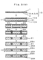
- FIG. 1 A sectional view of a mask film in an embodiment of the invention is described in Fig. 1.
- FIG. 2 A perspective view showing a mask film forming a parting layer and a non-parting portion in the embodiment of the invention is given in Fig. 2.
- the process sectional view of manufacturing method of two-sided circuit board using the mask film of the embodiment is shown in Fig. 3(a) and Fig. 3(b).
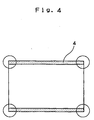
- the easily peeled portion of the mask film of the embodiment, and the non-parting portion or adhesive layer are show in a plan view in Fig. 4.
- a plan view and a sectional view showing the adhesion strength adjusting pattern in an embodiment of the invention are given in Fig. 5.
- a mask film 10 comprises a base material 1, a parting layer 2 and a non-parting portion 3 placed on the surface of the base material 1.
- the non-parting portion 3 can be adhered to a prepreg sheet 21.
- the non-parting portion 3 has an adhesive layer 4 as Shown in Fig. 4, or adhesion strength adjusting patterns 5,6 as shown in Fig. 5 and Fig. 6.
- a manufacturing method of two-side circuit board using the mask film 10 of the embodiment of the invention is described below.
- Fig. 3 (a) shows a manufacturing process of two-sided circuit board using the mask film 10 shown in Fig. 1.
- Fig. 3 (b) shows a manufacturing process of two-sided circuit board using the mask film 10 having adhesive layers 4, 5, 6 as shown in Fig. 4, Fig. 5 and Fig. 6.
- a mask film 10a is adhered to one side of a prepreg sheet 21 at a constant tension, and other mask film 10b is adhered to other side of the prepreg sheet 21.
- the thickness [t1] of the prepreg sheet 21 is about 150 ⁇ m.
- the prepreg sheet 21 has a nonwoven cloth, and a thermosetting resin impregnated in the nonwoven cloth. This thermosetting resin is not cured completely.
- the nonwoven cloth aromatic polyamide fiber, aramid fiber, glass fiber, ceramic fiber or other fiber having a high heat resisting temperature is used.
- the thermosetting resin for example, epoxy resin, melamine resin, or unsaturated polyester resin may be used. In this embodiment, the aramid fiber nonwoven cloth and epoxy resin were used.
- the parting layer 2 and non-parting portions 3, 4, 5, 6 are adhered to the surface of the prepreg sheet 21.
- the adhesion strength between the non-parting portion 3 and prepreg sheet 21 has a specified adhesion strength.
- the adhesion strength between the non-parting portion 3 and prepreg sheet 21 have an adjusted adhesion strength.
- Penetration holes 23 are formed in specified positions of the prepreg sheet 21 to which the mask films 10a, 10b are adhered, by laser processing method or the like.
- the penetration holes 23 are filled with conductive paste 24.
- the method of filling with conductive paste 24 comprises a step of plating the prepreg sheet 21 having penetration holes 23 on a table of a general printing press (not shown), and a step of applying the conductive paste 24 directly from above the mask film 10a by means of urethane rubber squeegee or the like.
- the mask films 10a, 10b play the role of printing mask and the role of prevention of contamination of the surface of the prepreg sheet 21.
- the mask films 10a, 10b are separated from both sides of the prepreg sheet 21.
- Metal foils 25a, 25b of Cu or the like are overlaid on both sides of the prepreg sheet 21.
- the metal foils 25a, 25b have a thickness of about 35 ⁇ m.
- the thickness of the prepreg sheet 21 is compressed.
- the thickness t2 of the prepreg sheet 21 after compression is about 100 ⁇ m, and the prepreg sheet 21 and metal foils 25a, 25b are mutually adhered.
- the metal foils 25a, 25b placed at both sides are electrically connected to the conductive paste 24 applied in the penetration holes 23 formed at specified positions. Further, by this heating and pressing, the thermosetting resin contained in the prepreg sheet 21 is completely cured.
- the both metal foils 25a, 25b are selectively etched, and circuit patterns 26a, 26b are formed.
- the metal foil 25a and metal foil 25b are electrically connected through the conductive paste applied in the penetration holes, and a two-sided circuit board is manufactured.
- the mask film 10 is further described below.
- the mask film 10 has a base material 1, and a parting layer 2 and a non-parting portion 3 formed on the surface of the base material.
- the base material 1 has a shape of 12 ⁇ m in thickness and 300 mm in width.
- the base material 1 is made of thermoplastic resin, such as polyethylene terephthalate (PET), polyphenylene sulfite (PPS), or polyethylene naphthalate (PEN). That is, the base material 1 has a property of being fused by heat.
- PET polyethylene terephthalate
- PPS polyphenylene sulfite
- PEN polyethylene naphthalate
- the parting layer 2 is placed in a region excluding the both ends along the length direction of the mask film 10.
- the parting layer 2 is made of a material not having melting point, for example, thermosetting resin or inorganic material. That is, the parting layer 2 has a property of not being fused by heat.
- the parting layer 2 is manufactured in the process comprising a step of preparing a paint having epoxy resin as main agent, melamine crosslinking agent as hardener, and methyl ethyl ketone (MEK) as solvent, and a step of applying the paint on the base film 1 by gravure process or the like so that the finish film thickness may be 1 ⁇ m, and drying and curing.
- MEK methyl ethyl ketone
- the non-parting portion 3 is formed at both ends along the length direction of the mask film 10.
- the non-parting portion 3 is formed simultaneously when the parting layer 2 is placed as shown in Fig. 2, by forming an unpainted portion not containing parting agent, on the roll gravure plate, at the step of forming the parting layer 2.
- the parting layer 2 and non-parting portion 3 are formed continuously.
- the base material 1 is exposed on the surface. Since the non-parting portion 3 does not have parting performance, at the step of adhering the mask film 10 and prepreg sheet 21, the same adhesion strength as when the base material 1 and prepreg sheet 21 are directly adhered is obtained.
- the adhesion strength between the mask film 10 and prepreg sheet 21 shown in Fig. 1 was measured in the conditions of 180-degree peel and measuring speed of 60 mm/min. As a result, the adhesion strength between the parting layer 2 and prepreg sheet 21 was about 0.5 g/10 mm. The adhesion strength of the non-parting portion 3 and prepreg sheet 21 was about 100 g/10 mm or more. Thus, the adhesion strength between the non-parting portion 3 and prepreg sheet 21 is stronger than the adhesion strength between the parting layer 2 and prepreg sheet 21.
- an adhesive layer 4 is placed in the non-parting portion 3.
- the easily peeling positions of the mask film 10 are four corners. At the four corners, the tension acts most strongly. Therefore, by placing the adhesive layer 4, the adhesion strength at the four corners is reinforced, and peeling between the mask film 10 and prepreg sheet 21 is prevented. Further, progress of peeling is arrested.
- the non-parting portion 3 is formed at both sides in the width direction of the mask film 10.
- the non-parting portion 3 may also have an adhesion strength adjusting pattern 5 as shown in Fig. 5 or Fig. 6.
- the adhesion strength adjusting pattern 5 consists of the non-parting portion 3 and parting layer 2 formed in pattern shapes alternately and continuously, parallel to the length direction of the base material 1.
- the adhesion strength adjusting pattern 5 consists of the non-parting portion 3 and parting layer 2 formed in pattern shapes alternately and discontinuously, orthogonal to the length direction of the base material 1.
- the adhesion strength of the non-parting portion 3 is too strong and separation of mask film is difficult at the step after filling with conductive paste, by the adhesion strength adjusting pattern 5 of the non-parting portion 3, the adhesion strength between the mask film 10 and prepreg sheet 21 can be freely adjusted. As a result, the mask film can be separated easily.
- the adhesion strength adjusting pattern 5 is not limited to the shapes shown in Fig. 5 and Fig. 6, but the adhesion strength adjusting pattern 5 can be formed in any pattern capable of adjusting the area of the non-parting portion 3.
- the adhesion strength adjusting pattern 5 includes, as shown in Fig. 6, an air invasion preventing portion 6 formed in a pattern shape formed parallel to the length direction of the base material 1.
- This air invasion preventing portion 6 formed parallel is formed continuously, or independently in part, or discontinuously. This configuration prevents invasion of air into the parting layer 2 due to peeling in the weak adhesive strength portion.
- the adhesion strength adjusting pattern 5 should have the pattern shapes of the non-parting portion 3 and parting layer 2 formed alternately and discontinuously, orthogonal to the length direction of the base material 1, and the air invasion preventing portion 6. This configuration prevents expansion of peel occurring due to passing of air among the patterns to push out to the central part of the parting layer 2 at the subsequent pressing and other steps.
- the surface properties of the parting layer 2 are reformed by surface treatment, such as corona process of applying corona discharge on the surface of the parting layer 2, or plasma process of applying plasma discharge.
- surface treatment such as corona process of applying corona discharge on the surface of the parting layer 2, or plasma process of applying plasma discharge.
- the surface tension of the parting layer 2 not having surface treatment is about 32 dynes.
- the surface tension of the parting layer 2 is 40 dynes. That is, the wettability of the parting layer 2 to the resin component in the prepreg sheet 21 is improved.
- the adhesion strength between the parting layer 2 and prepreg sheet 21 is about 0.5 g/10 mm.
- the adhesion strength between the parting layer 2 and prepreg sheet 21 is about 4 g/10 mm.
- the adhesion strength between the parting layer 2 and prepreg sheet 21 was measured in the condition of 180-degree peel and measuring speed of 60 mm/min.
- the base material 1 thermoplastic resin
- the parting layer 2 made of thermosetting resin not having melting point plays the role of barrier for preventing fusion of the base material 1 and prepreg sheet 21. Therefore, the fusing adhesion between base material 1 and prepreg sheet 21 is held to a minimum limit. Or, the fusing adhesion between base material 1 and prepreg sheet 21 is prevented.
- the peel strength is smaller, so that the mask film 10 can be easily separated from the prepreg sheet 21. That is, the generated impact peel is lessened by presence or absence of penetration holes. As a result, peeling of the resin component in the prepreg sheet, aramid fiber or conductive paste can be prevented.
- the penetration holes 23 should be formed in the parting layer 2.
- the penetration holes 23 are preferred to be formed in a region excluding the non-parting portion 3. In this constitution, no inconvenience occurs at the step of forming penetration holes by laser process, step of filling with conductive paste, or step of separating mask film. If the penetration holes 23 are formed in the non-parting portion 3, the base material and the prepreg sheet may be melted when forming penetration holes by heating process, and the resin component in the prepreg sheet, aramid fiber and conductive paste are likely to peel off at the step of separating the mask film 10 from the prepreg sheet 21.
- the peeling speed of the non-parting portion 3 is preferred to be lower than the peeling speed of the parting layer 2.
- the peeling speed of the non-parting portion 3 is about 20 mm/min, and the peeling speed of the parting layer 2 is 40 mm/min.
- the peeling speed of the mask film 10 is preferred to be low in both parting layer 2 and non-parting portion 3, and it is possible to separate stably in this case. It is preferred that the peeling speed be set in a range not to lower the productivity.
- the constitution and function of the mask film in the embodiment are explained below.
- the manufacturing method of the two-sided circuit board is same as in Exemplary Embodiment 1, and its explanation is omitted.
- a mask film 10 comprises a base material 1, a parting layer 2 placed on the surface of the base material, and an adhesive layer 4 placed on the parting layer 2.
- the base material 1 is made of cellophane material.
- the base material 1 is manufactured by casting a solution containing pulp.
- the base material 1 has a band shape of 20 ⁇ m in thickness and 300 mm in width.
- the parting layer 2 of about 1 ⁇ m in thickness is formed an the entire surface of one side of the base material 1.
- the adhesive layer 4 of about 0.3 ⁇ m in thickness is formed on the parting layer 2.
- the parting layer 2 is made of a thermosetting resin not having melting point.
- the placing method of the parting layer 2 comprises a step of applying a mixture of epoxy resin as main agent, melamine crosslinking agent as hardener, and methyl ethyl ketone (MEK) as solvent, on the surface of the base material 1 by gravure process or the like, and a step of drying and curing the applied mixture.
- the parting layer 2 has a film thickness of about 1 ⁇ m.
- the adhesive layer 4 is made of a material not have adhesiveness at room temperature, and having a fusing property when heated.
- the thermoplastic resin is preferred.
- thermoplastic resin include polyester or acrylic resin.
- the placing method of the adhesive layer 4 comprises a step of applying a mixture of thermoplastic resin and methyl ethyl ketone at a specified position of the parting layer 2, and a step of drying the applied mixture. In this process, the adhesive layer 4 is formed on both ends of the parting layer 2.
- the adhesion is small at ordinary temperature and it is easy to handle, and hence at the step of gluing with the prepreg sheet, the adhesive layer 4 is melted by heating and is easily adhered, and the adhesion strength is increased.
- the adhesion strength of the mask film and prepreg sheet thus manufactured in about 0.5 g/10 mm in the parting layer 2, and about 100 g/10 mm or more in the adhesive layer 4.
- the adhesion strength was measured in the condition of 180-degree peel and measuring speed of 60 m/min.
- the same effects as in Exemplary Embodiment 1 are obtained. That is, when this base material 1 is melted, the parting layer 2 made of the thermosetting resin not having melting point plays the role of prevention of the fusing adhesion between base material 1 and prepreg sheet 21. Therefore, the fusing adhesion between base material 1 and prepreg sheet 21 is held to a minimum limit. Or, fusion of base material 1 and prepreg sheet 21 is prevented. As a result, at the step of separating the mask film 10 from the prepreg sheet 21 after filling with conductive paste 24, the peel strength is smaller, and the mask film 10 can be easily separated from the prepreg sheet 21. As a result, peeling of resin component in the prepreg sheet, aramid fiber and conductive paste can be prevented.
- the penetration holes 23 should be formed in the parting layer 2.
- the penetration holes 23 are preferred to be formed in a region excluding the adhesive layer 4. In this constitution, no inconvenience occurs at the step of forming penetration holes by laser process, step of filling with conductive paste, and step of separating the mask film. If the penetration holes 23 are formed in the adhesive layer 4, the base material and the prepreg sheet are likely to be adhered when forming the penetration holes by heating process, and hence at the step of separating the mask film 10 from the prepreg sheet 21, the resin component in the prepreg sheet, aramid fiber and conductive paste are likely to be peeled off.
- the adhesive layer 4 has an adhesion strength adjusting pattern 5 as explained in Exemplary Embodiment 1.
- the adhesion strength adjusting pattern 5 has pattern shapes as shown in Fig. 5 or Fig. 6.
- the optimum adhesion strength between the mask film and prepreg sheet is maintained, and peeling of mask film and prepreg sheet is prevented. It further prevents the fusing adhesion between the mask film and prepreg sheet due to heat when forming the penetration holes, so that a circuit board having an excellent quality is obtained.
Landscapes
- Engineering & Computer Science (AREA)
- Manufacturing & Machinery (AREA)
- Microelectronics & Electronic Packaging (AREA)
- Non-Metallic Protective Coatings For Printed Circuits (AREA)
- Printing Elements For Providing Electric Connections Between Printed Circuits (AREA)
- Laminated Bodies (AREA)
- Laser Beam Processing (AREA)
- Shielding Devices Or Components To Electric Or Magnetic Fields (AREA)
Applications Claiming Priority (2)
| Application Number | Priority Date | Filing Date | Title |
|---|---|---|---|
| JP13672199A JP3344363B2 (ja) | 1999-05-18 | 1999-05-18 | マスクフィルムとその製造方法およびそれを用いた回路基板の製造方法 |
| JP13672199 | 1999-05-18 |
Publications (3)
| Publication Number | Publication Date |
|---|---|
| EP1054582A2 true EP1054582A2 (de) | 2000-11-22 |
| EP1054582A3 EP1054582A3 (de) | 2005-09-07 |
| EP1054582B1 EP1054582B1 (de) | 2006-09-27 |
Family
ID=15181951
Family Applications (1)
| Application Number | Title | Priority Date | Filing Date |
|---|---|---|---|
| EP00110617A Expired - Lifetime EP1054582B1 (de) | 1999-05-18 | 2000-05-18 | Maskenfilm, Verfahren zu dessen Herstellung, und Verfahren zur Herstellung einer Leiterplatte unter Verwendung desselben |
Country Status (6)
| Country | Link |
|---|---|
| US (2) | US6694612B1 (de) |
| EP (1) | EP1054582B1 (de) |
| JP (1) | JP3344363B2 (de) |
| CN (1) | CN1205845C (de) |
| DE (1) | DE60030908T2 (de) |
| TW (1) | TW491010B (de) |
Cited By (1)
| Publication number | Priority date | Publication date | Assignee | Title |
|---|---|---|---|---|
| US6694612B1 (en) * | 1999-05-18 | 2004-02-24 | Matsushita Electric Industrial Co., Ltd. | Mask film having a non-parting portion |
Families Citing this family (10)
| Publication number | Priority date | Publication date | Assignee | Title |
|---|---|---|---|---|
| JP4595284B2 (ja) * | 2003-01-28 | 2010-12-08 | 三菱瓦斯化学株式会社 | 炭酸ガスレーザーによる孔あけ用補助シート |
| US7251884B2 (en) * | 2004-04-26 | 2007-08-07 | Formfactor, Inc. | Method to build robust mechanical structures on substrate surfaces |
| DE102005062604A1 (de) * | 2005-12-27 | 2007-07-05 | Robert Bosch Gmbh | Verfahren zur Herstellung eines elektronischen Schaltungsträgers, Veredelungsvorrichtung eines elektronischen Schaltungsträgers sowie Schaltungsträger |
| JP2009076699A (ja) * | 2007-09-20 | 2009-04-09 | Fujikura Ltd | 多層プリント配線板の製造方法 |
| JP5173358B2 (ja) * | 2007-10-31 | 2013-04-03 | 東邦テナックス株式会社 | 保護フィルム付プリプレグ |
| CN102405692A (zh) * | 2009-04-02 | 2012-04-04 | 松下电器产业株式会社 | 电路基板的控制方法及电路基板 |
| CN101976716A (zh) * | 2010-10-21 | 2011-02-16 | 光颉科技股份有限公司 | 基板通孔的导电方法 |
| JP5110613B2 (ja) * | 2010-11-25 | 2012-12-26 | 東洋アルミ千葉株式会社 | 樹脂ベース基板用離型材およびその製造方法 |
| TWI489342B (zh) * | 2012-12-26 | 2015-06-21 | Ind Tech Res Inst | 凹版轉印組合物及凹版轉印製程 |
| JP6431649B1 (ja) * | 2017-07-13 | 2018-11-28 | 株式会社寺岡製作所 | 多層マスキングシート |
Family Cites Families (13)
| Publication number | Priority date | Publication date | Assignee | Title |
|---|---|---|---|---|
| GB1478341A (en) * | 1973-06-07 | 1977-06-29 | Hitachi Chemical Co Ltd | Printed circuit board and method of making the same |
| US4915983A (en) * | 1985-06-10 | 1990-04-10 | The Foxboro Company | Multilayer circuit board fabrication process |
| US4642160A (en) * | 1985-08-12 | 1987-02-10 | Interconnect Technology Inc. | Multilayer circuit board manufacturing |
| JP2601128B2 (ja) | 1992-05-06 | 1997-04-16 | 松下電器産業株式会社 | 回路形成用基板の製造方法および回路形成用基板 |
| US5358604A (en) * | 1992-09-29 | 1994-10-25 | Microelectronics And Computer Technology Corp. | Method for producing conductive patterns |
| JP2768236B2 (ja) | 1993-10-08 | 1998-06-25 | 松下電器産業株式会社 | 多層基板の製造方法 |
| US5505321A (en) * | 1994-12-05 | 1996-04-09 | Teledyne Industries, Inc. | Fabrication multilayer combined rigid/flex printed circuit board |
| JP3400164B2 (ja) * | 1995-01-23 | 2003-04-28 | 三井金属鉱業株式会社 | 多層プリント配線板およびその製造方法 |
| US5902438A (en) * | 1997-08-13 | 1999-05-11 | Fry's Metals, Inc. | Process for the formation of anisotropic conducting material |
| US6120693A (en) * | 1998-11-06 | 2000-09-19 | Alliedsignal Inc. | Method of manufacturing an interlayer via and a laminate precursor useful for same |
| US6163957A (en) * | 1998-11-13 | 2000-12-26 | Fujitsu Limited | Multilayer laminated substrates with high density interconnects and methods of making the same |
| JP3344363B2 (ja) * | 1999-05-18 | 2002-11-11 | 松下電器産業株式会社 | マスクフィルムとその製造方法およびそれを用いた回路基板の製造方法 |
| JP3903701B2 (ja) * | 2000-08-17 | 2007-04-11 | 松下電器産業株式会社 | 多層回路基板とその製造方法 |
-
1999
- 1999-05-18 JP JP13672199A patent/JP3344363B2/ja not_active Expired - Fee Related
-
2000
- 2000-04-26 TW TW089107884A patent/TW491010B/zh not_active IP Right Cessation
- 2000-05-17 CN CNB001089269A patent/CN1205845C/zh not_active Expired - Fee Related
- 2000-05-18 US US09/573,826 patent/US6694612B1/en not_active Expired - Fee Related
- 2000-05-18 DE DE60030908T patent/DE60030908T2/de not_active Expired - Lifetime
- 2000-05-18 EP EP00110617A patent/EP1054582B1/de not_active Expired - Lifetime
-
2003
- 2003-01-09 US US10/338,642 patent/US7066344B2/en not_active Expired - Fee Related
Cited By (2)
| Publication number | Priority date | Publication date | Assignee | Title |
|---|---|---|---|---|
| US6694612B1 (en) * | 1999-05-18 | 2004-02-24 | Matsushita Electric Industrial Co., Ltd. | Mask film having a non-parting portion |
| US7066344B2 (en) | 1999-05-18 | 2006-06-27 | Matsushita Electric Industrial Co., Ltd. | Mask film, its manufacturing method, and manufacturing method of circuit board using the same |
Also Published As
| Publication number | Publication date |
|---|---|
| JP2000332375A (ja) | 2000-11-30 |
| US20030153197A1 (en) | 2003-08-14 |
| EP1054582B1 (de) | 2006-09-27 |
| CN1274257A (zh) | 2000-11-22 |
| US7066344B2 (en) | 2006-06-27 |
| EP1054582A3 (de) | 2005-09-07 |
| DE60030908D1 (de) | 2006-11-09 |
| US6694612B1 (en) | 2004-02-24 |
| JP3344363B2 (ja) | 2002-11-11 |
| CN1205845C (zh) | 2005-06-08 |
| TW491010B (en) | 2002-06-11 |
| DE60030908T2 (de) | 2007-01-04 |
Similar Documents
| Publication | Publication Date | Title |
|---|---|---|
| US6459046B1 (en) | Printed circuit board and method for producing the same | |
| EP2164311B1 (de) | Leiterplatte und verfahren zu ihrer herstellung | |
| US6451710B1 (en) | Method of manufacturing multi-layer printed wiring board | |
| US7572500B2 (en) | Method of manufacturing circuit-forming board and material of circuit-forming board | |
| EP1054582B1 (de) | Maskenfilm, Verfahren zu dessen Herstellung, und Verfahren zur Herstellung einer Leiterplatte unter Verwendung desselben | |
| JP2002064269A (ja) | 多層回路基板とその製造方法 | |
| TWI292290B (de) | ||
| WO2002034023A1 (en) | Circuit forming board producing method, circuit forming board, and material for circuit forming board | |
| JP2874581B2 (ja) | 回路基板の製造方法 | |
| US5460680A (en) | Method for manufacturing multi-layer printed board | |
| JP4147723B2 (ja) | プリント配線板 | |
| JP3956667B2 (ja) | 回路基板およびその製造方法 | |
| JP2650072B2 (ja) | 多層プリント配線板の製造方法 | |
| JPH07106760A (ja) | 多層基板の製造方法 | |
| JP3738536B2 (ja) | プリント配線基板の製造方法 | |
| KR102436612B1 (ko) | 다층인쇄회로기판의 최외층 형성 방법 | |
| JP4433531B2 (ja) | 導電性バンプを備えたプリント基板の製造方法 | |
| JP5287075B2 (ja) | 回路基板の製造方法 | |
| US8069557B2 (en) | Method of manufacturing circuit forming board | |
| JP2000013018A (ja) | 回路形成基板の製造方法とその製造装置および回路形成基板用材料 | |
| JP2005116935A (ja) | 回路形成基板の製造用材料 | |
| JP5287074B2 (ja) | 剥離きっかけ形成装置およびそれを用いた剥離きっかけ形成方法 | |
| JP3414229B2 (ja) | プリント配線板の製造方法 | |
| JP2002094233A (ja) | 回路基板の製造方法 | |
| KR20110116848A (ko) | 인쇄회로기판의 제조 방법 |
Legal Events
| Date | Code | Title | Description |
|---|---|---|---|
| PUAI | Public reference made under article 153(3) epc to a published international application that has entered the european phase |
Free format text: ORIGINAL CODE: 0009012 |
|
| AK | Designated contracting states |
Kind code of ref document: A2 Designated state(s): AT BE CH CY DE DK ES FI FR GB GR IE IT LI LU MC NL PT SE |
|
| AX | Request for extension of the european patent |
Free format text: AL;LT;LV;MK;RO;SI |
|
| PUAL | Search report despatched |
Free format text: ORIGINAL CODE: 0009013 |
|
| AK | Designated contracting states |
Kind code of ref document: A3 Designated state(s): AT BE CH CY DE DK ES FI FR GB GR IE IT LI LU MC NL PT SE |
|
| AX | Request for extension of the european patent |
Extension state: AL LT LV MK RO SI |
|
| 17P | Request for examination filed |
Effective date: 20050920 |
|
| GRAP | Despatch of communication of intention to grant a patent |
Free format text: ORIGINAL CODE: EPIDOSNIGR1 |
|
| AKX | Designation fees paid |
Designated state(s): DE FI FR GB |
|
| GRAS | Grant fee paid |
Free format text: ORIGINAL CODE: EPIDOSNIGR3 |
|
| GRAA | (expected) grant |
Free format text: ORIGINAL CODE: 0009210 |
|
| AK | Designated contracting states |
Kind code of ref document: B1 Designated state(s): DE FI FR GB |
|
| REG | Reference to a national code |
Ref country code: GB Ref legal event code: FG4D |
|
| REF | Corresponds to: |
Ref document number: 60030908 Country of ref document: DE Date of ref document: 20061109 Kind code of ref document: P |
|
| ET | Fr: translation filed | ||
| PLBE | No opposition filed within time limit |
Free format text: ORIGINAL CODE: 0009261 |
|
| STAA | Information on the status of an ep patent application or granted ep patent |
Free format text: STATUS: NO OPPOSITION FILED WITHIN TIME LIMIT |
|
| 26N | No opposition filed |
Effective date: 20070628 |
|
| PGFP | Annual fee paid to national office [announced via postgrant information from national office to epo] |
Ref country code: GB Payment date: 20140514 Year of fee payment: 15 |
|
| PGFP | Annual fee paid to national office [announced via postgrant information from national office to epo] |
Ref country code: DE Payment date: 20140515 Year of fee payment: 15 Ref country code: FI Payment date: 20140512 Year of fee payment: 15 Ref country code: FR Payment date: 20140509 Year of fee payment: 15 |
|
| REG | Reference to a national code |
Ref country code: DE Ref legal event code: R119 Ref document number: 60030908 Country of ref document: DE |
|
| GBPC | Gb: european patent ceased through non-payment of renewal fee |
Effective date: 20150518 |
|
| PG25 | Lapsed in a contracting state [announced via postgrant information from national office to epo] |
Ref country code: FI Free format text: LAPSE BECAUSE OF NON-PAYMENT OF DUE FEES Effective date: 20150518 |
|
| REG | Reference to a national code |
Ref country code: FR Ref legal event code: ST Effective date: 20160129 |
|
| PG25 | Lapsed in a contracting state [announced via postgrant information from national office to epo] |
Ref country code: GB Free format text: LAPSE BECAUSE OF NON-PAYMENT OF DUE FEES Effective date: 20150518 Ref country code: DE Free format text: LAPSE BECAUSE OF NON-PAYMENT OF DUE FEES Effective date: 20151201 |
|
| PG25 | Lapsed in a contracting state [announced via postgrant information from national office to epo] |
Ref country code: FR Free format text: LAPSE BECAUSE OF NON-PAYMENT OF DUE FEES Effective date: 20150601 |