EP1055903B1 - Procédé optique de mesure d'épaisseur de couches et d'autres propriétés d'objets tels que des plaquettes semiconductrices - Google Patents
Procédé optique de mesure d'épaisseur de couches et d'autres propriétés d'objets tels que des plaquettes semiconductrices Download PDFInfo
- Publication number
- EP1055903B1 EP1055903B1 EP00304118A EP00304118A EP1055903B1 EP 1055903 B1 EP1055903 B1 EP 1055903B1 EP 00304118 A EP00304118 A EP 00304118A EP 00304118 A EP00304118 A EP 00304118A EP 1055903 B1 EP1055903 B1 EP 1055903B1
- Authority
- EP
- European Patent Office
- Prior art keywords
- radiation
- optical
- optical radiation
- characteristic
- layer
- Prior art date
- Legal status (The legal status is an assumption and is not a legal conclusion. Google has not performed a legal analysis and makes no representation as to the accuracy of the status listed.)
- Expired - Lifetime
Links
- 230000003287 optical effect Effects 0.000 title claims description 176
- 238000000034 method Methods 0.000 title claims description 59
- 239000004065 semiconductor Substances 0.000 title claims description 17
- 235000012431 wafers Nutrition 0.000 title description 68
- 230000005855 radiation Effects 0.000 claims description 219
- 238000012545 processing Methods 0.000 claims description 29
- 238000002310 reflectometry Methods 0.000 claims description 25
- 230000007480 spreading Effects 0.000 claims description 24
- 238000003892 spreading Methods 0.000 claims description 24
- 229910052751 metal Inorganic materials 0.000 claims description 21
- 239000002184 metal Substances 0.000 claims description 21
- 239000000758 substrate Substances 0.000 claims description 18
- 230000008569 process Effects 0.000 claims description 9
- 238000005498 polishing Methods 0.000 claims description 8
- 230000008859 change Effects 0.000 claims description 4
- 238000001914 filtration Methods 0.000 claims description 2
- 230000000903 blocking effect Effects 0.000 claims 2
- 238000005259 measurement Methods 0.000 description 39
- 239000013307 optical fiber Substances 0.000 description 16
- 239000000463 material Substances 0.000 description 14
- RYGMFSIKBFXOCR-UHFFFAOYSA-N Copper Chemical compound [Cu] RYGMFSIKBFXOCR-UHFFFAOYSA-N 0.000 description 11
- 229910052802 copper Inorganic materials 0.000 description 11
- 239000010949 copper Substances 0.000 description 11
- 238000005286 illumination Methods 0.000 description 10
- 230000000694 effects Effects 0.000 description 8
- 238000011065 in-situ storage Methods 0.000 description 8
- 239000002002 slurry Substances 0.000 description 8
- 238000004364 calculation method Methods 0.000 description 6
- 239000007788 liquid Substances 0.000 description 6
- 238000012544 monitoring process Methods 0.000 description 6
- 229910052715 tantalum Inorganic materials 0.000 description 6
- GUVRBAGPIYLISA-UHFFFAOYSA-N tantalum atom Chemical compound [Ta] GUVRBAGPIYLISA-UHFFFAOYSA-N 0.000 description 6
- 230000004888 barrier function Effects 0.000 description 4
- 230000008901 benefit Effects 0.000 description 4
- 239000004020 conductor Substances 0.000 description 4
- 239000000969 carrier Substances 0.000 description 3
- 238000004891 communication Methods 0.000 description 3
- 239000011162 core material Substances 0.000 description 3
- 238000001514 detection method Methods 0.000 description 3
- 238000011161 development Methods 0.000 description 3
- 238000012625 in-situ measurement Methods 0.000 description 3
- 239000002245 particle Substances 0.000 description 3
- 239000000126 substance Substances 0.000 description 3
- 238000012360 testing method Methods 0.000 description 3
- XUIMIQQOPSSXEZ-UHFFFAOYSA-N Silicon Chemical compound [Si] XUIMIQQOPSSXEZ-UHFFFAOYSA-N 0.000 description 2
- 230000002411 adverse Effects 0.000 description 2
- 230000015572 biosynthetic process Effects 0.000 description 2
- 238000005229 chemical vapour deposition Methods 0.000 description 2
- 238000009792 diffusion process Methods 0.000 description 2
- 238000005530 etching Methods 0.000 description 2
- 239000005337 ground glass Substances 0.000 description 2
- 238000000691 measurement method Methods 0.000 description 2
- 230000004044 response Effects 0.000 description 2
- 229910052710 silicon Inorganic materials 0.000 description 2
- 239000010703 silicon Substances 0.000 description 2
- 238000001039 wet etching Methods 0.000 description 2
- 229910052782 aluminium Inorganic materials 0.000 description 1
- XAGFODPZIPBFFR-UHFFFAOYSA-N aluminium Chemical compound [Al] XAGFODPZIPBFFR-UHFFFAOYSA-N 0.000 description 1
- 230000001427 coherent effect Effects 0.000 description 1
- 239000010987 cubic zirconia Substances 0.000 description 1
- 230000003247 decreasing effect Effects 0.000 description 1
- 239000003989 dielectric material Substances 0.000 description 1
- 238000009826 distribution Methods 0.000 description 1
- 238000001312 dry etching Methods 0.000 description 1
- 230000009977 dual effect Effects 0.000 description 1
- 230000005670 electromagnetic radiation Effects 0.000 description 1
- 238000009713 electroplating Methods 0.000 description 1
- 230000007613 environmental effect Effects 0.000 description 1
- 239000000835 fiber Substances 0.000 description 1
- 239000011521 glass Substances 0.000 description 1
- 238000000227 grinding Methods 0.000 description 1
- 238000009434 installation Methods 0.000 description 1
- 238000004519 manufacturing process Methods 0.000 description 1
- 238000007620 mathematical function Methods 0.000 description 1
- 239000007769 metal material Substances 0.000 description 1
- 150000002739 metals Chemical class 0.000 description 1
- 230000004048 modification Effects 0.000 description 1
- 238000012986 modification Methods 0.000 description 1
- 238000001020 plasma etching Methods 0.000 description 1
- 229910021420 polycrystalline silicon Inorganic materials 0.000 description 1
- 229920005591 polysilicon Polymers 0.000 description 1
- 238000003672 processing method Methods 0.000 description 1
- 239000010453 quartz Substances 0.000 description 1
- 229910052594 sapphire Inorganic materials 0.000 description 1
- 239000010980 sapphire Substances 0.000 description 1
- 238000007789 sealing Methods 0.000 description 1
- VYPSYNLAJGMNEJ-UHFFFAOYSA-N silicon dioxide Inorganic materials O=[Si]=O VYPSYNLAJGMNEJ-UHFFFAOYSA-N 0.000 description 1
- 238000004441 surface measurement Methods 0.000 description 1
- 239000012780 transparent material Substances 0.000 description 1
Images




Classifications
-
- B—PERFORMING OPERATIONS; TRANSPORTING
- B24—GRINDING; POLISHING
- B24B—MACHINES, DEVICES, OR PROCESSES FOR GRINDING OR POLISHING; DRESSING OR CONDITIONING OF ABRADING SURFACES; FEEDING OF GRINDING, POLISHING, OR LAPPING AGENTS
- B24B37/00—Lapping machines or devices; Accessories
- B24B37/005—Control means for lapping machines or devices
- B24B37/013—Devices or means for detecting lapping completion
-
- B—PERFORMING OPERATIONS; TRANSPORTING
- B24—GRINDING; POLISHING
- B24B—MACHINES, DEVICES, OR PROCESSES FOR GRINDING OR POLISHING; DRESSING OR CONDITIONING OF ABRADING SURFACES; FEEDING OF GRINDING, POLISHING, OR LAPPING AGENTS
- B24B49/00—Measuring or gauging equipment for controlling the feed movement of the grinding tool or work; Arrangements of indicating or measuring equipment, e.g. for indicating the start of the grinding operation
- B24B49/02—Measuring or gauging equipment for controlling the feed movement of the grinding tool or work; Arrangements of indicating or measuring equipment, e.g. for indicating the start of the grinding operation according to the instantaneous size and required size of the workpiece acted upon, the measuring or gauging being continuous or intermittent
- B24B49/04—Measuring or gauging equipment for controlling the feed movement of the grinding tool or work; Arrangements of indicating or measuring equipment, e.g. for indicating the start of the grinding operation according to the instantaneous size and required size of the workpiece acted upon, the measuring or gauging being continuous or intermittent involving measurement of the workpiece at the place of grinding during grinding operation
-
- B—PERFORMING OPERATIONS; TRANSPORTING
- B24—GRINDING; POLISHING
- B24B—MACHINES, DEVICES, OR PROCESSES FOR GRINDING OR POLISHING; DRESSING OR CONDITIONING OF ABRADING SURFACES; FEEDING OF GRINDING, POLISHING, OR LAPPING AGENTS
- B24B49/00—Measuring or gauging equipment for controlling the feed movement of the grinding tool or work; Arrangements of indicating or measuring equipment, e.g. for indicating the start of the grinding operation
- B24B49/12—Measuring or gauging equipment for controlling the feed movement of the grinding tool or work; Arrangements of indicating or measuring equipment, e.g. for indicating the start of the grinding operation involving optical means
-
- G—PHYSICS
- G01—MEASURING; TESTING
- G01B—MEASURING LENGTH, THICKNESS OR SIMILAR LINEAR DIMENSIONS; MEASURING ANGLES; MEASURING AREAS; MEASURING IRREGULARITIES OF SURFACES OR CONTOURS
- G01B11/00—Measuring arrangements characterised by the use of optical techniques
- G01B11/02—Measuring arrangements characterised by the use of optical techniques for measuring length, width or thickness
- G01B11/06—Measuring arrangements characterised by the use of optical techniques for measuring length, width or thickness for measuring thickness ; e.g. of sheet material
- G01B11/0616—Measuring arrangements characterised by the use of optical techniques for measuring length, width or thickness for measuring thickness ; e.g. of sheet material of coating
- G01B11/0625—Measuring arrangements characterised by the use of optical techniques for measuring length, width or thickness for measuring thickness ; e.g. of sheet material of coating with measurement of absorption or reflection
-
- G—PHYSICS
- G01—MEASURING; TESTING
- G01N—INVESTIGATING OR ANALYSING MATERIALS BY DETERMINING THEIR CHEMICAL OR PHYSICAL PROPERTIES
- G01N21/00—Investigating or analysing materials by the use of optical means, i.e. using sub-millimetre waves, infrared, visible or ultraviolet light
- G01N21/17—Systems in which incident light is modified in accordance with the properties of the material investigated
- G01N21/47—Scattering, i.e. diffuse reflection
- G01N21/4738—Diffuse reflection, e.g. also for testing fluids, fibrous materials
Definitions
- This invention relates generally to techniques for determining conditions of surfaces, and, more specifically, to doing so by measuring a characteristic of the reflectivity and/or emissivity of surfaces.
- An example application is the measurement of the thickness of a film on a substrate, such as a film that is formed or removed from a semiconductor wafer during the fabrication of integrated circuits. The thickness measurement is made either simultaneously with the film processing (in situ) or thereafter (in line). More specific applications include in situ measurements of the thickness of a film being reduced or removed by techniques such as wet etching, plasma etching, spin etching or chemical-mechanical-polishing (CMP).
- CMP chemical-mechanical-polishing
- 5,695,660 measures the thickness or level of planarization of both dielectric and metal layers in situ by optical or thermal techniques during etching or CMP, including making the measurements through the back side of the wafer.
- CMP chemical vapor deposition
- an optical signal communicates with a wafer being processed through an optical window provided in one of the moving elements such as the wafer carrier.
- PCT published international
- WO 97/25660 multiple sensors are carried by a moving component ofa CMP machine, with a wireless communication of measurements and control signals provided between the sensors and a host control station.
- Other patent documents of interest include U.S. patents nos. 5,138,149, 5,190,614, 5,166,525, 5,292,605, 5,308,447, 5,362,969, 5,717,608 and 5,786,886, and PCT publication no. WO93/25893.
- the present invention is directed at further improvements to methods and instruments for optically measuring characteristics of surfaces, such as surfaces of circuit structures partially formed on semiconductor wafers or flat panel displays.
- a method of determining a particular characteristic of a surface area comprises:
- Apparatus according to the invention comprises:
- Methods and apparatus of the invention can be used to monitor the effects CMP processing, and for measuring the thickness of layers of dielectric, semiconductor or metal materials carried by a substrate.
- the invention seeks to enable the foregoing functions simultaneously with processing the surface or layer being monitored (in situ).
- An example would be to measure the changing thickness of a layer carried by a substrate, such as a semiconductor wafer, while being processed (in situ) to increase or decrease the layer thickness.
- a surface being monitored in a typical application of the invention is illuminated by optical radiation with rays of the incident radiation spread over a wide angle to form a radiation field modified by the surface that is also collected over a wide angle and detected by a sensor.
- the angles of optical radiation illumination and collection are made sufficiently wide so that variations in an optical path and/or of the surface being monitored, other than of the surface optical characteristic of interest, that occur over time or between different copies of the surface are minimized or substantially eliminated in order to improve the accuracy of the resultant measurements.
- the incident radiation is spread over an angle of at least 45 degrees and up to 180 degrees when striking the surface being monitored, and is also collected over an angle of 45 degrees or more, and up to 180 degrees. As the illumination angle is increased, the collection angle can be made narrower.
- the collected radiation is detected, and the detected radiation is processed to monitor a desired characteristic of the surface.
- Specific structures of sensors include use of an optical radiation spreading element, such as a diffuser or multi-pass reflector, positioned near to the surface being monitored, and an optical collection element, such as an end of an optical fiber or a lens, is positioned to receive the spread radiation after being modified by the surface, such as by reflection from the surface. Random or pseudo-random scattering of the illumination radiation is preferred, such as occurs when the optical radiation incident on the surface being monitored has passed through ground glass.
- the wide angle illumination and detection significantly reduces the effects of variations in scattering of the optical signals that can occur independently of the quantity desired to be measured.
- the incident optical radiation, and that modified by the surface being monitored can be scattered varying amounts that depend upon the surface, angles that the radiation strikes the surface and optical elements, changes over time, and other causes. If narrow angles are viewed, for example, any variation in the amount of incident radiation that is scatted into the narrow viewing angle because of differences in scattering properties across the surface being monitored or between different surfaces, versus that which is scattered over wider angles out of view, causes the detected optical signal to vary. Significant variations can also occur when the surface is being viewed through a liquid layer, such as an etchant or slurry, that changes its thickness and other characteristics over time.
- optical radiation is used in this application to mean electromagnetic radiation in a continuous wavelength range including visible and near visible infrared and ultraviolet wavelengths, generally considered to extend from about 0.2 to about 4 microns.
- Monitoring the optical radiation modified by a surface usually also includes monitoring the level of radiation incident upon the surface so that the reflectivity or emissivity of the surface, or a related quantity, can be calculated either as the ultimate surface characteristic to be determined or as an intermediate quantity used to calculate some other surface characteristic.
- resulting calculations of the reflectivity or emissivity of the surface are highly meaningful because they are independent of changing conditions unrelated to surface reflectivity and emissivity.
- the calculation of emissivity is preferred because it is understood in the scientific community to be independent of the geometry, wavelength and other factors that can cause undesired variations in optical measurements.
- a layer of material being formed on or removed from a substrate, in whole or in part, is being monitored, it is preferably illuminated and viewed in the above described manner.
- An endpoint to the complete removal of a layer is one characteristic of the surface that may be determined.
- Another characteristic is the thickness of the layer, either in relative or absolute terms. Because surface reflectivity or emissivity is being determined with the effects of varying measurement conditions being minimized, the thickness of a layer can be determined with a high degree of accuracy by a look-up table, model or other relationship between the reflectivity or emissivity and thickness.
- the monitored layer is a metal or other generally opaque material
- its reflectivity and emissivity are directly related to the thickness of the layer if the layer is thin enough to be at least partially transparent.
- the layer's reflectivity or emissivity when measured by the techniques summarized above, is directly related to the thickness of the metal layer once it has become thin enough to be semi-transparent.
- a metal film on a semiconductor wafer is semi-transparent when its thickness is less than about 500 to 1500 Angstroms (50 to 150 nm), depending on the metal and the wavelength of radiation used.
- the thicknesses can be determined from a look-up table or set of functions that relate the measured reflectivity or emissivity with the layer's thickness. This makes it possible to measure and control the thicknesses of thin metal films with precision. Once the metal film is completely removed, then the optical properties being measured are those of the layers under the metal film. The measurement of the reflectivity or emissivity of a metal layer can be conducted with one or more wavelengths of optical radiation.
- the thickness of a layer of transparent material can be monitored throughout a range of its entire thickness by viewing a signal resulting from interference of a portion of the incident optical radiation reflected from an outside surface from which material is being removed and another portion of the incident radiation reflected from some other interface in the structure of the substrate and layer.
- a given table or set of functions are used to relate specific values of the interference signal with layer thicknesses.
- Interference signals are preferably generated in at least two different wavelengths of optical radiation. Precise measurements of the thickness of a transparent layer are then obtainable without ambiguity under many circumstances when the two or more optical radiation wavelengths and ranges of layer thicknesses are suitable. In other cases, such precision additionally requires knowledge of the approximate layer thickness, as determined by observation or otherwise, in order to obtain a precise measurement of the transparent layer's thickness without ambiguity.
- the radiation can be generated by separate narrow bandwidth radiation sources, such as light emitting diodes (LEDs), and then the uniquely responsive to one of the source wavelengths.
- the two or more radiation sources are each modulated with a unique frequency.
- Electrical signals obtained from a single or multiple radiation receiving photodetectors are then filtered to pass the source modulating frequencies in order to obtain a separate signal for each of the illumination wavelengths.
- the frequencies of modulation are preferably selected to be different from that of any ambient radiation or electrical noise that might be present in the environment in which the measurements are being taken, thereby to significantly reduce adverse effects of any such ambient radiation and noise.
- the radiation source modulation and photodetector signal filtering technique can also be used when a single optical radiation is directed at the surface being monitored in order to similarly reduce the effects of any ambient radiation and electrical noise that might be present at different frequencies from the modulating frequency.
- CMP CMP
- substrates such as semiconductor wafers
- a slurry of abrasive particles and a chemical etchant is usually also used on the pad.
- One or more optical radiation sensors are installed in either the carrier, if the processing is being viewed from the back side of the substrates, or in the platen, if being viewed from the front side of the substrates.
- the front side of the wafers can also be periodically viewed in some CMP machines when the wafers are being loaded into or unloaded from the CMP machine, or are periodically moved off the platen within the CMP machine during the CMP process.
- An analog signal obtained from a sensor installed in a CMP machine platen is a continuous one, resulting from being scanned across the one or more wafers held by the carrier and the surface of the carrier in between the wafers. If the reflectivity and emissivity of the carrier surface is significantly different than that of the wafers, there is a significant discontinuity of the signal obtained by the photodetector as its view crosses an edge of the wafer. Discrete measurements of the wafer surface are referenced to these discontinuities as a way of identifying the positions of the measurements. In some cases it is desired to take specific measurements near an edge of the wafer outside of patterned circuit die, and in others it is desired to take specific measurements over a patterned location. Control of the location is made possible by use of the edge discontinuity. The measurements at specific positions of the wafers are then monitored over time in order to measure the effect of the processing on the wafer surface.
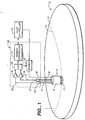
- a substrate or other object 11 contains a surface 13 that is being measured.
- An optical sensor head 15 directs optical radiation from one or more light emitting diodes (LEDs) against a spot 17 of the surface 13.
- LEDs light emitting diodes
- Other sources of optical radiation can be used instead ofLEDs but it is preferred that they have a narrow bandwidth, such as a few dozen nanometers in wavelength, or less. Highly coherent sources of optical radiation are unnecessary.
- a portion of the source radiation that is reflected from the surface is gathered by suitable optics, such as an optical fiber 19.
- Other optics, such as an optical fiber 21 collects a portion of the source radiation, preferably without any significant amount of radiation reflected from the surface, as background radiation that is used as a. reference.
- the sensor head 15 is connected with a module 23 that includes optical and electronic elements to interface between the sensor 15 and a host controller 25, such as a personal computer.
- Photodetectors 27 and 29 receive the optical signals from the optical fibers 19 and 21, respectively, to generate electrical signals in respective lines 31 and 33. These electrical signals are amplified by respective amplifiers 35 and 37, whose outputs are connected with an analog-to-digital converter 39. The amplified and digitized outputs of the photodetectors 27 and 29 and then sent to a controller 41 which controls operation of the sensor 15 and of the module 23, and can make a portion or all of the calculations necessary to determine the ultimate quantity related to the characteristic of the surface 13 that is being measured.
- the module 23 also includes a power circuit 43 that supplies, through a line 45, the LEDs or other optical radiation source included within the sensor head 15.
- the power is supplied by the host controller 25 but controlled by the controller 41.
- the module 23 is preferably provided in a small rugged package so that it may be positioned near the head 15 in a piece of processing machinery.
- a diameter of the sensor head 15 of about one-half of one inch is preferred for the CMP applications described below, resulting in a spot 17 having a diameter something less than that, depending upon the optical elements at the end of the head 15.
- Measurements can be made at a single point of the surface 13, at multiple points, or continuously across the surface 13, such as along a path 47, by providing relative motion between the head 15 and surface 13. Either the head 15 can be moved, or the substrate 11 moved, or both. In the CMP application described below, both are moved.
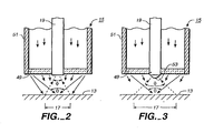
- Figure 2 shows a conceptual cross-sectional view of an end portion of the sensor head 15.
- Optical radiation from the source(s) (not shown in Figures 2 and 3) contained in the head 15 is directed through an optical radiation spreading element that extends across an end opening of a cylindrical housing 51.
- the element 49 spreads the source radiation over a maximum angle ⁇ , preferably with substantially uniform intensity.
- a diffraction element may be made for this purpose but use of ground glass for the element 49 operates satisfactorily and provides a randomness to the surface illumination. As discussed above, better results are obtained as the angle ⁇ increases.
- the element 49 is designed to provide this angle to be at least 45 degrees.
- An end of an optical fiber has an acceptance angle of optical radiation that depends primarily upon the refractive index of the fiber core material.
- Such an angle ⁇ is shown on Figure 2 at an end of the optical fiber 19, which extends through the element 49 to have an unobstructed view of the surface 13. It is also desirable that this angle be made as large as is practical, as discussed above, preferably 45 degrees or more.
- An optical fiber with a core made of sapphire, quartz ) or cubic zirconia has an angle of acceptance of about 45 degrees.
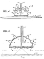
- a lens element 53 can be added to the end of the optical fiber 19, as shown in Figure 3.
- the diameter of the area viewed by the optical fiber 19 is increased, as indicated in Figure 3. It is the area of the surface 13 within the angle of acceptance ⁇ that defines the spot 17, assuming that this area is also substantially uniformly illuminated.
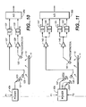
- FIG. 4 and 5 One specific embodiment of a sensor head 15 is shown in Figures 4 and 5, where elements that are counterparts of those described above are identified by the same reference numbers but, when different in structure, have a prime (') added to the reference number.
- a plurality of LEDs 55-64 are distributed around a hemispherical shell 65.
- a transparent cover 67 may be provided with radiation scattering properties but a wide distribution of radiation results from the numerous LEDs and internal reflection within the shell 65.
- the surface 13 is illuminated with a range of angles close to 180 degrees, depending upon the distance between the shell and the surface 13. Lenses provided as part of the LEDs may also be roughened to add to the diffusion of the illumination provided by the head 15 of Figures 4 and 5.
- FIG. 6 Another specific embodiment of a sensor head 15, which is preferred, is shown in cross section in Figure 6.
- a plurality of LEDs including LEDs 71 and 73, carried by a flat plate extending across the inside of the shell. Radiation from the LEDs passes through a diffuser 77 through which the radiation gathering optical fiber 19 extends, similar to the structure of Figures 2 and 3.
- the sensor head 15" When used in hostile environments, such as in semiconductor liquid etch or CMP machines, the sensor head 15" is sealed against liquids, moisture and gas vapors. This can be done at one end by sealing the diffuser 77 to sensor head 15" but a better seal is obtained by adding a single piece clear glass plate 79 which extends completely across and is sealed to the inside of the shell 51.
- Optical radiation from the LEDs is gathered into the optical fiber 17 by positioning a circular diffusive reflecting element 81 around the optical fiber 19.
- the element 81 is made small enough so as not to block the diffuser 77 from receiving almost all of the radiation from the LEDs but large enough to reflect enough of the radiation into the optical fiber 17 to obtain a useful background reference signal.
- the wavelength of the optical radiation source is chosen to be the best for monitoring the particular surface characteristics of interest.
- the radiation needs to interact with the feature or characteristic of the object or its surface that is desired to be monitored, in a way that can be detected in the radiation after being modified by the object.
- wavelengths slightly below the band edge of silicon are usually best, generally infra-red radiation less than one micron, to which the wafer is opaque. If radiation is transmitted through the object being monitored to obtain an object modified beam that is detected, the radiation is, of course, chosen to be of a wavelength that will pass through the object.
- the controller 41 calculates a ratio of the reflected radiation signal from the photodetector 27 to the background radiation signal from the photodetector 29, as is well known.
- the instrument is first calibrated by positioning the sensor head 15 against at least one surface having a known reflectivity, and preferably against several surfaces having known different reflectivities. Calibration includes adjusting the relative gains of the two signal channels until the instrument reads the known reflectivity of the test surface. This is preferably done by software within the controller 41, particularly when multiple test surfaces are used.
- emissivity of a surface is calculated as a measure of the thickness of a layer of material that forms that surface.
- the primary application is in semiconductor processing but the techniques are not so limited.
- a changing thickness of a dielectric material which is transparent to the incident radiation, is monitored by measuring the interference of the radiation reflected from both surfaces of the layer. The interference signal passes through peaks and valleys as the layer either becomes thicker when being formed by chemical vapor deposition (CVD) or otherwise, or becomes thinner as material is removed by wet or dry etching, CMP or some other technique.
- FIG. 7 shows a modification of the single wavelength embodiments described above.
- Two different types ofLEDs 91 and 92 emit optical radiation at wavelengths ⁇ 1 and ⁇ 2, respectively. This is reflected off the surface 13 and gathered by an optical fiber 93, passed to a beam splitter 95 and thence to photodetectors 97 and 99 through respective optical bandpass filters 101 ( ⁇ 1) and 103 ( ⁇ 2). The signal outputs of these photodetectors are then digitized by the analog-to-digital converter 39'.
- the reference radiation is obtained by an optical fiber 105 which directs the radiation sampled from the LEDs 91 and 92 to a beam splitter 107. A portion of the reference radiation then strikes a photodetector 109 through an optical filter 113 that passes ⁇ 1, and another portion reaches a photodetector 111 through an optical filter 115 that passes ⁇ 2.
- the electrical outputs of these photodetectors are also applied to the analog-to-digital converter 39'.
- the controller 41 ( Figure 1) now calculates the reflectivity or emissivity of the surface 13 separately for each of the radiation wavelengths ⁇ 1 and ⁇ 2.
- Calculated emissivity data are shown in curves of Figure 8. These curves are the same when the layer is being increased in thickness as when it is being decreased.
- One interference curve 117 results from processing the signals from the ⁇ 1 receiving photodetectors 97 and 109, and a second interference curve 119 is obtained from the signals from the ⁇ 2 receiving photodetectors 99 and 111.
- the calculation of emissivity described above is made twice, once for each wavelength.
- Additional data can be acquired for a third or more distinct wavelengths, thus giving one or more additional interference curves, but the complexity of implementing such a system generally outweighs the advantages of doing so.
- the periods of the curves 117 and 119 are different because of the different wavelengths at which the data is acquired. Their peaks and valleys are thus not aligned. This allows the thickness of the transparent layer of the surface 13 to be determined from the data forming both of the curves 117 and 119.
- the two values of the curves are unique for each value of layer thickness, at least over a significant range of thicknesses.
- the table of Figure 9 illustrates this.
- Each of the pairs of emissivity values for the two wavelengths corresponds to a specific thickness of the layer being monitored.
- the thickness of the layer is (A).
- A the thickness of the layer is (B).
- B a combination of values from the curves 117 and 119 of v and x gives a thickness (B).
- the table of Figure 9 is empirically determined for a specific layer material. An instrument that is capable of measuring the thickness of two or more types of materials has a separate look-up table for each material.
- ambient radiation can exist in the processing machine or environment in which the measurements are taken. This can, of course, affect the accuracy of the surface measurements.
- the measuring instrument can be shielded from such optical radiation in many cases, its effect can alternatively be effectively eliminated by modulating the incident radiation at a frequency other than that at which the ambient radiation may be modulated. That is, the power supply frequency and harmonics (60, 120 Hz. etc. in the U.S.) are avoided. Frequencies of any electrical noise generated in the processing machinery, which can be induced into the measurement circuits carrying low level signals, are also avoided.
- the photodetector output is then applied to an electronic bandpass filter to pass a narrow band of frequencies around the modulating frequency.
- Such a technique is shown in Figure 10, wherein the power supply 43a to an LED 121 is modulated with a sinusoidal signal having a frequency f1, such as several hundred Hz., depending on the situation.
- Background and reflected radiation photodetectors 121 and 123 apply their electrical signal to respective amplifiers 127 and 129.
- the amplified signals are then passed through respective filters 131 and 133 having narrow pass bands around the frequency f1.
- the electrical outputs of the filters 131 and 133 therefore represent the optical signals resulting from illumination by the LED 121 without optical or electrical noise introduced by the environment.
- Some characteristic of the filtered alternating current signals such as their root-mean-square (rms), is taken as representative of the surface characteristic being measured, before further arithmetic processing.
- This LED modulation technique can also be adapted to serve an additional function in a multiple wavelength instrument, as a variation of the embodiment of Figure 7.
- Figure 11 shows LEDs 135 and 137, emitting optical radiation at respective distinct wavelengths ⁇ 1 and ⁇ 2, being modulated at respective distinct frequencies f1 and f2.
- electrical bandpass filters are used. Only one reference radiation photodetector 139 is used, and only one photodetector 141 receives LED radiation reflected from the surface 13. Photodetector outputs are amplified by pre-amplifiers 143 and 145.
- the amplified signal from the photodetector 139 is applied to two filters 147 and 149, which each pass narrow frequency bands around one of the LED modulating frequencies f1 and f2, respectively.
- the amplified signal from the photodetector 141 is applied to two filters 151 and 153, which pass the frequencies f1 and f2, respectively.
- the four filter outputs are then digitized by the analog-to-digital converter 39b.
- the controller 41 ( Figure 1) then processes the signals from the f1 bandpass filters 147 and 151 to obtain data for one of the curves of Figure 8, and also processes the signals from the f2 bandpass filters 149 and 153 to obtain data for the other curve.
- the optical detection of films of normally opaque materials such as metals has typically been limited to determining when a breakthrough occurs during removal of the film by detecting when the amplitude of reflected radiation changes from one level to another in response to the metal being totally removed.
- a measurement of the reflectivity or emissivity of a metal layer can provide a measurement of its thickness when very thin.
- the shape of the curve in Figure 12 is for a copper layer over a layer of tantalum, as an example, the combination of which is carried by another material, usually a dielectric, on a substrate. Copper is used for conductors in integrated circuits.
- the layer of tantalum, or some other appropriate material provides a barrier to prevent copper from diffusing into the underlying dielectric.
- the emissivity of the two layer structure when at their full thicknesses, is a ( Figure 12), but when the copper layer is very thin, between thicknesses (X) and (Y), its emissivity varies in a measurable manner between a and b, as a function of its thickness.
- the thickness at (X) is about 1,000 Angstroms (100 nm).
- the underlying tantalum is thin enough to not be completely opaque, its emissivity also varying in a measurable manner between levels b and c as a function of its thickness, as indicated between thicknesses (Y) and (Z) in Figure 12.
- the emissivity c is that of the material under the tantalum, usually a dielectric.
- Such thin layers of metal are becoming extensively used in semiconductor processing and structures.
- the techniques of the present invention may be used to measure thickness of thin metal layers in situ during their formation, thinning or complete removal from all or portions of a wafer.
- a dielectric layer is formed to cover the wafer except where contacts need to be made through the dielectric layer to aluminum, polysilicon, substrate diffusions and the like. Shallow trenches are formed in the dielectric to define where the copper conductors are to be placed.
- a thin (typically 200-800 Angstroms i.e. 20-80 nm barrier layer, such as tantalum, is then deposited over the entire dielectric, including the trenches and vias through the dielectric.
- a copper layer is then formed, usually by electroplating, over the barrier layer. CMP is then used to remove the copper and underlying barrier layer from the top surface of the dielectric, leaving them in the trenches and vias where the copper conductors are desired to remain.
- Figure 13 is a look-up table that provides empirically determined data relating the emissivity and layer thickness of the curve of Figure 12. Measurements of emissivity, made by one of the ways described previously, are then converted to thickness by use of such a look-up table.
- the dual wavelength and modulated source techniques may also be used with metal layers.
- the thickness of a thin metal layer when in a region such as between (X) and (Y) of Figure 12, can be carefully controlled both during its formation and during its removal.
- the data of that characteristic curve are monitored from right to left, and when the layers are being removed, from left to right. It is also useful to monitor the thickness of a layer when it is being totally removed since this can give the process controller or the operator an indication when that end point is about to be reached.
- a very significant application of the various aspects of the present invention is the in situ measurement of layer thickness during its removal, at least partially, by CMP.
- CMP The largest application of CMP is in semiconductor wafer processing.
- CMP machines There are many different types of CMP machines being used and contemplated for use in the future. They provide relative motion with pressure between the layer surface and a pad, with a slurry of liquid chemical etchant and abrasive particles between them. It is difficult to optically monitor processes of such machines in situ because of the complex motion usually given to the substrate and layer being measured, limited optical access and optically hostile environment.
- Figures 14 and 15 show installation of a film thickness monitor according to the present invention on a CMP machine.
- Wafers 161 and 163 carry respective layers 165 and 167 that are being reduced in thickness.
- the backsides of the wafers are attached to respective wafer carriers 169 and 171.
- the wafer carriers are rotated by respective electrical motors 173 and 175.
- a structure 177 holds the wafer carriers in position.
- the wafer layers are urged against a pad 179 that is attached to a round platen 181 that itself is rotated by an electrical motor 183.
- a layer 185 of a liquid chemical etchant and abrasive particles in a slurry is applied to the pad 179. Material is removed from exposed surfaces of the wafer layers 165 and 167 by grinding them across the pad 179 with the abrasive slurry between them.
- the sensor head 15 described above preferably the version shown in Figure 6, is installed in the platen 181 in a position to reflect light off of the layers being processed as they move over the head 15.
- a transparent window 187 is installed in the pad 179 over the sensor 15.
- Optical radiation generated within the head 15 then travels upward through the window 187, through the slurry 185, strikes the wafer layers in turn that are being processed, and returns back through the same path to the gathering optics within the head 15.
- the head electronics 23 is attached underneath the platen 181. Communication of its digital output signals and control signals with the host controller 25 can occur through a slip-ring assembly 189 on a rotating shaft 191 of the platen 181. Alternatively, wireless communication can be utilized, such as with the use of infra-red or radio frequency frequencies.
- the optical path between the sensor head 15 and the wafer layer being monitored is not unencumbered.
- the slurry 185 although largely transparent to the interrogating radiation, affects the optical radiation that must pass through it twice, once in each direction.
- the sensor head of the present invention overcomes this difficulty to provide good measurements.
- the wide angle radiation illumination and collection, as described above, minimizes adverse effects of the changing optical properties of the slurry over time, particularly changing radiation scattering.
- the present invention thereby makes it possible to accurately measure the thickness of the layers being processed, while they are being processed.
- Figure 15 shows the platen 181 with the position in space of the wafers 161 and 163, as well as additional wafers 162 and 164, shown in dotted outline.
- Each of the four wafers is rotated in the direction indicated with arrows by its individual driving motor.
- the direction of rotation of the platen 15 is also indicated by an arrow.
- the sensor head 15 is thus scanned in a path 193 across all four rotating wafers, one at a time.
- An example emissivity signal obtained from the sensor head electronics 23 ( Figure 1) is shown in Figure 16A.
- This signal provides the emissivity (or, alternately, can be the reflectivity, if desired) of each wafer in turn as it is being scanned by the sensor 15, with the emissivity (or reflectivity) level of some other portion(s) of the CMP machine being measured as the sensor 15 moves between wafers.
- a rotational position encoder 195 attached to the rotating platen shaft 191 is read by a sensor 197, from which the host controller 25 generates relative position pulses such as those shown in Figure 16B.
- the encoder and sensor 195 and 197 can be of any suitable mechanical, optical, magnetic or other known type.
- the position pulses have a purpose of allowing the host controller to correlate the received data with an individual wafer.
- the host controller 25 can easily separate the stream of data obtained from the sensor head electronics 23, as shown in Figure 16, into separate signals, that from the wafers and that from the portions of the processing machine in between the wafers. This is because of a sharp change in emissivity level that will normally occur as the sensor head 15 passes across an edge of a wafer. For example, such a change occurs at a signal edge 201 as the sensor head 15 passes across an edge of the wafer 161 and onto the wafer. As the sensor head 15 leaves the wafer 161, passing from it to view some other surface, an edge 203 in the signal of Figure 16A occurs. As the processing of the wafer 161 proceeds, the measured level of its emissivity changes, for example, between two levels 205 and 207.
- a signal 209 is indicated for a given wafer location a defined distance from a wafer edge. This wafer location can be selected, for example, to be where integrated circuits are formed, or, alternatively, nearer wafer edges where integrated circuits are not formed.
- the signal 209 varies over time, in a manner of the examples of Figures 8 and 12. Each time the sensor head 15 passes over the location of the waver 161 where the signal 209 is taken, a new emissivity data point is acquired for that location. Monitored data may be selected by the host controller 25 for each of the other three wafers that have the same position with respect to their edges as the data 209 of the wafer 161. By using such a common location, the layer thickness may be compared among wafers.
- Non-uniform processing shows as a variation of the data 205 in a single span, for example, between the edges 201 and 203.
- Statistical calculations can be made by the host processor 25 of data from a particular wafer to provide an indication of a spread of the emissivity values across that wafer, either from a single scan or from multiple scans across it. Further, polishing rates may be calculated from the emissivity data, either at one or more specific wafer locations with respect to an edge or on the average across a portion or the entire wafer.
Landscapes
- Engineering & Computer Science (AREA)
- Mechanical Engineering (AREA)
- Physics & Mathematics (AREA)
- General Physics & Mathematics (AREA)
- Health & Medical Sciences (AREA)
- Life Sciences & Earth Sciences (AREA)
- Chemical & Material Sciences (AREA)
- Analytical Chemistry (AREA)
- Biochemistry (AREA)
- General Health & Medical Sciences (AREA)
- Immunology (AREA)
- Pathology (AREA)
- Length Measuring Devices By Optical Means (AREA)
Claims (36)
- Procédé permettant de déterminer une caractéristique particulière d'une surface, comportant les étapes consistant à :positionner à une première distance par rapport à la surface un élément optique d'étalement du rayonnement (49) qui étale un rayonnement optique incident sur un angle d'au moins 45 degrés ;diriger le rayonnement optique en provenance d'au moins une source de rayonnement optique jusque sur l'élément optique d'étalement du rayonnement (49) et de là sur la surface afin de faire réfléchir le rayonnement étalé en provenance de la surface ;capturer, par le biais de l'élément optique d'étalement du rayonnement (49), un rayonnement optique réfléchi par la surface, la première optique de convergence de rayonnement (19) ayant un angle d'admission d'au moins 45 degrés et positionnée à une deuxième distance par rapport à ladite surface par le positionnement d'une extrémité d'un premier conduit de lumière à la deuxième distance par rapport à la surface ;capturer le rayonnement optique en provenance de la au moins une source de rayonnement, la deuxième optique de convergence de rayonnement (17, 21) étant positionnée afin de recevoir le rayonnement optique en provenance de la au moins une source de rayonnement par le positionnement d'une extrémité d'un deuxième conduit de lumière afin de recevoir le rayonnement optique en provenance de la au moins une source de rayonnement ;détecter le rayonnement optique capturé par la première optique de convergence de rayonnement et par la deuxième optique de convergence de rayonnement ; etdéterminer la caractéristique particulière de la surface d'après les niveaux du rayonnement optique détecté en provenance de chacune de la première optique de convergence de rayonnement et de la deuxième optique de convergence de rayonnement.
- Procédé selon la revendication 1, dans lequel l'étape consistant à capturer le rayonnement optique en provenance de ladite au moins une source de rayonnement comprend l'étape consistant à faire réfléchir une portion du rayonnement optique en provenance de ladite au moins une source de rayonnement jusque dans l'extrémité du deuxième conduit de lumière d'un diffuseur de rayonnement optique réfléchissant qui est positionné sur une trajectoire de rayonnement optique en provenance de ladite au moins une source de rayonnement optique.
- Procédé selon la revendication 1 ou la revendication 2, dans lequel la caractéristique particulière de la surface comprend sa réflectivité, et l'étape consistant à déterminer la réflectivité comprend l'étape consistant à prendre un rapport d'un niveau détecté du rayonnement optique capturé par le premier conduit de lumière et par le deuxième conduit de lumière.
- Procédé selon la revendication 1 ou la revendication 2, dans lequel la caractéristique particulière de la surface comprend son émissivité, et l'étape consistant à déterminer l'émissivité comprend l'étape consistant à prendre un rapport d'un niveau détecté de rayonnement optique capturé par le premier conduit de lumière et par le deuxième conduit de lumière.
- Procédé selon la revendication 1 ou la revendication 2, dans lequel la surface se prolonge en travers d'un film porté par un substrat, et la caractéristique particulière du film devant être déterminée comprend son épaisseur, et l'étape consistant à déterminer l'épaisseur du film comprend l'étape consistant à comparer un niveau détecté de rayonnement optique capturé par le premier conduit de lumière et par le deuxième conduit de lumière.
- Procédé selon l'une quelconque des revendications précédentes, dans lequel la surface se prolonge en travers d'une structure formée sur une plaquette semi-conductrice.
- Procédé selon l'une quelconque des revendications 1 à 5, dans lequel la surface se prolonge en travers d'une structure formée sur un affichage à écran plat.
- Procédé selon la revendication 7, qui de plus comporte l'étape consistant à maintenir ladite surface contre une surface d'un élément mobile, et dans lequel l'étape consistant à diriger le rayonnement sur la surface comprend l'étape consistant à diriger le rayonnement en provenance de ladite au moins une source de rayonnement et au travers du diffuseur se trouvant à l'intérieur de l'élément mobile.
- Procédé selon l'une quelconque des revendications 1 à 7, dans lequel la caractéristique particulière de la surface est déterminée de manière simultanée avec la surface traitée d'une manière qui change sa dite caractéristique particulière.
- Procédé selon la revendication 9, dans lequel la surface est traitée par polissage chimico-mécanique.
- Procédé selon l'une quelconque des revendications 1 à 7, dans lequel l'étape consistant à positionner l'élément optique d'étalement du rayonnement comprend l'étape consistant à positionner un diffuseur de rayonnement transparent (77) à la première distance par rapport à la surface.
- Procédé selon l'une quelconque des revendications 1 à 7, dans lequel l'étape consistant à positionner l'élément optique d'étalement du rayonnement comprend l'étape consistant à positionner un élément hémisphérique ayant une pluralité de sources de rayonnement optique maintenues autour d'une surface intérieure de celui-ci, surface intérieure qui est réfléchissante et positionnée afin de s'ouvrir sur la surface.
- Procédé selon l'une quelconque des revendications 1 à 7, dans lequel l'étape consistant à diriger le rayonnement optique jusque sur l'élément optique d'étalement du rayonnement en provenance d'au moins une source de rayonnement optique comprend l'étape consistant à diriger ledit rayonnement en provenance d'au moins une source de rayonnement optique d'une première largeur de bande et d'au moins une source de rayonnement optique d'une deuxième largeur de bande, ladite première largeur de bande et ladite deuxième largeur de bande étant distinctes l'une par rapport à l'autre.
- Procédé selon la revendication 13, dans lequel les sources de rayonnement optique de la première largeur de bande sont excitées à une première fréquence de modulation, les sources de rayonnement optique de la deuxième largeur de bande sont excitées à une deuxième fréquence de modulation qui est distincte de la première fréquence de modulation, dans lequel l'étape consistant à détecter le rayonnement optique comprend l'étape consistant à diriger le rayonnement optique capturé par le biais de la première optique de convergence de rayonnement (19) sur un photodétecteur (27), et dans lequel l'étape consistant à déterminer la caractéristique de la surface comprend l'étape consistant à diriger un signal de sortie électrique en provenance du photodétecteur au travers de filtres passe-bande qui passent respectivement ladite première fréquence de modulation et ladite deuxième fréquence de modulation.
- Procédé selon la revendication 5, dans lequel l'étape consistant à diriger le rayonnement optique jusque sur l'élément optique d'étalement du rayonnement comprend l'étape consistant à diriger ledit rayonnement en provenance d'au moins une source de rayonnement optique d'une première largeur de bande et d'au moins une source de rayonnement optique d'une deuxième largeur de bande, ladite première largeur de bande et ladite deuxième largeur de bande étant distinctes l'une par rapport à l'autre, dans lequel le film est transparent au rayonnement optique de ladite première largeur de bande et de ladite deuxième largeur de bande, et de plus comportant:l'étape consistant à maintenir une relation de valeurs d'épaisseur du film en fonction des paires de valeurs des données de la caractéristique optique au niveau de la première largeur de bande et de la deuxième largeur de bande, etl'étape consistant à convertir de manière répétitive les paires mesurées de valeurs de la caractéristique optique au niveau de la première largeur de bande et de la deuxième largeur de bande respectives par des valeurs d'épaisseur de couche en référence à ladite relation.
- Procédé selon la revendication 5, dans lequel le film est du métal, et de plus comportant :l'étape consistant à maintenir une relation de valeurs d'épaisseur du film en fonction de soit la réflectivité soit l'émissivité dans une région où le film métallique devient partiellement transparent au rayonnement optique en provenance desdites une ou plusieurs sources de rayonnement optique, etl'étape consistant à convertir de manière répétitive les paires mesurées de valeurs de la caractéristique optique au niveau de la première largeur de bande et de la deuxième largeur de bande respectives par des valeurs d'épaisseur de couche en référence à ladite relation.
- Procédé selon l'une quelconque de la revendication 15 ou de la revendication 16, dans lequel les étapes consistant à déterminer la caractéristique de couche sont exécutées de manière simultanée, le film étant réduit en épaisseur par le biais d'un processus de polissage chimico-mécanique.
- Procédé selon l'une quelconque des revendications 1 à 7, dans lequel l'étape consistant à diriger le rayonnement optique jusque sur l'élément optique d'étalement du rayonnement comprend l'étape consistant à moduler le rayonnement optique en provenance desdites une ou plusieurs sources de rayonnement optique à une fréquence donnée, dans lequel l'étape consistant à détecter le rayonnement optique comprend l'étape consistant à diriger le rayonnement optique capturé par la première optique de convergence de rayonnement sur un photodétecteur (27) et dans lequel l'étape consistant à déterminer la caractéristique de la surface comprend l'étape consistant à diriger un signal de sortie électrique en provenance du photodétecteur au travers d'un filtre passe-bande qui passe ladite fréquence de modulation donnée.
- Procédé selon l'une quelconque des revendications 1 à 7, comportant de plus l'étape consistant à se déplacer de manière répétitive en travers de la surface sur laquelle le rayonnement optique est dirigé en provenance desdites une ou plusieurs sources de rayonnement optique et en provenance de laquelle le rayonnement optique réfléchi en provenance de celle-ci est capturé, l'étape consistant à noter un changement au niveau du rayonnement optique détecté causé par une discontinuité sur la surface, et l'étape consistant à référencer une région sur la surface dans une certaine position par rapport à la discontinuité pour laquelle ladite caractéristique particulière de la surface est déterminée.
- Procédé selon la revendication 1, dans lequel l'étape consistant à détecter le rayonnement optique comporte l'étape consistant à acquérir les données d'une caractéristique optique d'une couche ayant ladite surface à au moins une première longueur d'onde et une deuxième longueur d'onde distinctes de rayonnement optique, dans lequel ladite caractéristique optique varie différemment en fonction de l'épaisseur de la couche à ladite première longueur d'onde et à ladite deuxième longueur d'onde,
l'étape consistant à maintenir une relation de valeurs d'épaisseur de la couche en fonction des paires de valeurs des données de la caractéristique optique au niveau de la première longueur d'onde et de la deuxième longueur d'onde, et
l'étape consistant à convertir de manière répétitive les paires mesurées de valeurs de la caractéristique optique au niveau de la première longueur d'onde et de la deuxième longueur d'onde respectives par des valeurs d'épaisseur de couche en référence à ladite relation, ladite étape consistant à convertir ayant lieu de manière simultanée avec le processus de changement de l'épaisseur de la couche. - Procédé selon la revendication 20, dans lequel l'étape consistant à diriger le rayonnement optique comprend l'étape consistant à éclairer la surface avec le rayonnement optique comprenant ladite première longueur d'onde et ladite deuxième longueur d'onde distinctes, et dans lequel l'étape consistant à acquérir les données d'une caractéristique optique comporte l'étape consistant à recevoir une portion du rayonnement d'éclairage réfléchi en provenance de la couche, et l'étape consistant à détecter le rayonnement réfléchi d'une manière permettant de procurer des signaux séparés connexes aux niveaux du rayonnement réfléchi au niveau de ladite première longueur d'onde et de ladite deuxième longueur d'onde.
- Procédé selon la revendication 21, dans lequel l'étape consistant à détecter le rayonnement optique comprend l'étape consistant à mettre en oeuvre un premier photodétecteur et un deuxième photodétecteur sur la trajectoire du rayonnement réfléchi avec un premier filtre passe-bande optique et un deuxième filtre passe-bande optique respectifs devant ceux-ci, ledit premier filtre passant le rayonnement optique de la première longueur d'onde tout en bloquant le rayonnement optique de la deuxième longueur d'onde et le deuxième filtre passant le rayonnement optique au niveau de la deuxième longueur d'onde tout en bloquant le rayonnement optique au niveau de la première longueur d'onde.
- Procédé selon la revendication 21, dans lequel l'étape consistant à éclairer la surface comprend l'étape consistant à moduler le rayonnement d'éclairage de ladite première longueur d'onde et de ladite deuxième longueur d'onde au niveau d'une première fréquence et d'une deuxième fréquence distinctes respectives, et dans lequel l'étape consistant à détecter le rayonnement optique comprend l'étape consistant à obtenir un signal de sortie électrique de photodétecteur de celui-ci et l'étape consistant à filtrer ledit signal électrique afin de passer les composantes de celui-ci qui sont connexes aux valeurs du signal optique au niveau de ladite première fréquence et de ladite deuxième fréquence.
- Procédé selon la revendication 20, dans lequel la caractéristique optique de la couche pour laquelle les données sont acquises comprend une émissivité de la couche.
- Procédé selon la revendication 20, dans lequel l'étape consistant à maintenir la relation des valeurs comprend l'étape consistant à maintenir un tableau de paires de valeurs de la caractéristique optique au niveau de ladite au moins première longueur d'onde et de ladite au moins deuxième longueur d'onde pour chacune d'une pluralité d'épaisseurs de ladite couche, et l'étape consistant à convertir les paires mesurées de valeurs de la caractéristique optique par des valeurs d'épaisseur de couche comprend l'étape consistant à consulter l'épaisseur de couche dans ce tableau.
- Procédé selon l'une quelconque des revendications 21 à 23, dans lequel l'étape consistant à éclairer la surface comprend de plus l'étape consistant à diriger le rayonnement optique contre la surface sur un angle de 45 degrés ou plus et l'étape consistant à recevoir le rayonnement réfléchi en provenance de la couche comprend l'étape consistant à recevoir ledit rayonnement sur un angle de 45 degrés ou plus.
- Procédé selon la revendication 26, dans lequel la caractéristique optique de la couche pour laquelle les données sont acquises comprend une réflectivité de la couche.
- Procédé selon la revendication 26, dans lequel la caractéristique optique de la couche pour laquelle les données sont acquises comprend une émissivité de la couche
- Procédé selon l'une quelconque des revendications 20 à 24, dans lequel le traitement étant effectué sur ladite couche est un polissage chimico-mécanique.
- Appareil permettant de déterminer une caractéristique réfléchissante d'une zone d'un article, comportant :une composante de machine (181) ayant une surface (179) adaptée pour être contactée par ledit article,une fenêtre (187) formant une portion de la surface de ladite composante,au moins une source de rayonnement optique portée par la composante sur un côté de la fenêtre de manière opposée par rapport à la surface entrant en contact avec l'article,un élément optique d'étalement du rayonnement (49) porté par la composante entre la fenêtre et ladite au moins une source de rayonnement optique, ledit élément étalant la lumière en provenance de ladite au moins une source de rayonnement optique à travers la fenêtre sur un angle de 45 degrés ou plus,un premier conduit de lumière porté par la composante qui se prolonge au travers de l'élément d'étalement avec une extrémité faisant face à la fenêtre afin de converger le rayonnement optique passant au travers de ladite fenêtre en provenance de la zone de l'article, ladite extrémité du premier conduit de lumière ayant un angle d'admission de 45 degrés ou plus,un premier photodétecteur (27) porté par la composante afin de recevoir le rayonnement optique dans le premier conduit de lumière et de produire un premier signal électrique connexe à celui-ci,un deuxième conduit de lumière porté par la composante et ayant une extrémité positionnée entre ladite au moins une source de rayonnement optique et l'élément d'étalement afin d'obtenir le rayonnement optique en provenance de ladite au moins une source de rayonnement optique,un deuxième photodétecteur (29) porté par la composante afin de recevoir le rayonnement dans le deuxième conduit de lumière et de produire un deuxième signal électrique connexe à celui-ci, etun processeur (25) utilisant le premier signal électrique et le deuxième signal électrique afin de déterminer la caractéristique réfléchissante de la zone de l'article.
- Appareil selon la revendication 30, comportant de plus un deuxième élément d'étalement de rayonnement (81) porté par la composante entre la fenêtre et ladite au moins une source de rayonnement optique en une position permettant de diriger le rayonnement optique en provenance de ladite au moins une source de rayonnement optique jusque dans l'extrémité du deuxième conduit de lumière.
- Appareil selon la revendication 31, dans lequel la surface entrant en contact avec l'article de la composante est plane et a une surface arrière définissant une épaisseur de l'élément entre celles-ci, et dans lequel tous parmi la fenêtre, au moins une source de rayonnement optique, l'élément d'étalement, le deuxième élément d'étalement du rayonnement optique, l'extrémité du premier conduit de lumière, et l'extrémité du deuxième conduit de lumière, sont positionnés dans un compartiment formé dans la composante entre sa dite surface entrant en contact avec l'article et sa dite surface arrière.
- Appareil selon la revendication 32, dans lequel un module électronique (23) est attaché à ladite composante de machine qui comprend des amplificateurs (27, 29) pour chacun du premier signal électrique et du deuxième signal électrique, un circuit de conversion analogique-numérique (39), et un processeur (25), une sortie du processeur procurant les données de la caractéristique réfléchissante de la zone de l'article devant être déterminée.
- Appareil selon la revendication 33, dans lequel la composante de machine peut être déplacée afin de traiter l'article.
- Appareil selon l'une quelconque des revendications 30 à 33, dans lequel la composante fait partie d'une machine de polissage chimico-mécanique qui est mise en mouvement lors du traitement de la zone de l'article.
- Appareil selon la revendication 35, dans lequel la composante est un plateau muni d'un tampon à polir alors que sa dite surface est adaptée pour mise en contact par ledit article.
Applications Claiming Priority (2)
| Application Number | Priority Date | Filing Date | Title |
|---|---|---|---|
| US09/317,697 US6570662B1 (en) | 1999-05-24 | 1999-05-24 | Optical techniques for measuring layer thicknesses and other surface characteristics of objects such as semiconductor wafers |
| US317697 | 1999-05-24 |
Publications (2)
| Publication Number | Publication Date |
|---|---|
| EP1055903A1 EP1055903A1 (fr) | 2000-11-29 |
| EP1055903B1 true EP1055903B1 (fr) | 2006-12-20 |
Family
ID=23234867
Family Applications (1)
| Application Number | Title | Priority Date | Filing Date |
|---|---|---|---|
| EP00304118A Expired - Lifetime EP1055903B1 (fr) | 1999-05-24 | 2000-05-16 | Procédé optique de mesure d'épaisseur de couches et d'autres propriétés d'objets tels que des plaquettes semiconductrices |
Country Status (4)
| Country | Link |
|---|---|
| US (2) | US6570662B1 (fr) |
| EP (1) | EP1055903B1 (fr) |
| DE (1) | DE60032411T2 (fr) |
| TW (1) | TW577974B (fr) |
Cited By (1)
| Publication number | Priority date | Publication date | Assignee | Title |
|---|---|---|---|---|
| KR20220136342A (ko) * | 2019-11-18 | 2022-10-07 | 투룬 일리오피스토 | 수분 센서, 연마 디바이스 및 연마 패드 내의 수분을 측정하기 위한 방법 |
Families Citing this family (28)
| Publication number | Priority date | Publication date | Assignee | Title |
|---|---|---|---|---|
| US6320609B1 (en) | 1998-07-10 | 2001-11-20 | Nanometrics Incorporated | System using a polar coordinate stage and continuous image rotation to compensate for stage rotation |
| US6368881B1 (en) * | 2000-02-29 | 2002-04-09 | International Business Machines Corporation | Wafer thickness control during backside grind |
| DE10123470B4 (de) * | 2001-05-15 | 2010-08-19 | Carl Zeiss Jena Gmbh | Verfahren und Anordnung zur berührungslosen Ermittlung von Produkteigenschaften |
| US20030045008A1 (en) * | 2001-08-31 | 2003-03-06 | Gregory Olsen | Method and apparatus for monitoring changes in the surface of a workpiece during processing |
| US6842235B2 (en) * | 2001-09-28 | 2005-01-11 | Infineon Technologies North America Corp. | Optical measurement of planarized features |
| IL145699A (en) * | 2001-09-30 | 2006-12-10 | Nova Measuring Instr Ltd | Method of thin film characterization |
| US6935922B2 (en) | 2002-02-04 | 2005-08-30 | Kla-Tencor Technologies Corp. | Methods and systems for generating a two-dimensional map of a characteristic at relative or absolute locations of measurement spots on a specimen during polishing |
| US6762849B1 (en) * | 2002-06-19 | 2004-07-13 | Novellus Systems, Inc. | Method for in-situ film thickness measurement and its use for in-situ control of deposited film thickness |
| US6709312B2 (en) | 2002-06-26 | 2004-03-23 | Motorola, Inc. | Method and apparatus for monitoring a polishing condition of a surface of a wafer in a polishing process |
| DE10319543B4 (de) * | 2003-04-30 | 2011-03-03 | Byk-Gardner Gmbh | Vorrichtung und Verfahren zur Bestimmung von Oberflächeneigenschaften |
| WO2005017489A2 (fr) * | 2003-07-11 | 2005-02-24 | Svt Associates, Inc. | Systeme de mappage de couches |
| US7204639B1 (en) * | 2003-09-26 | 2007-04-17 | Lam Research Corporation | Method and apparatus for thin metal film thickness measurement |
| CN101006491A (zh) * | 2004-09-27 | 2007-07-25 | Idc公司 | 测量和建模显示器中的功率消耗 |
| US20060176487A1 (en) * | 2004-09-27 | 2006-08-10 | William Cummings | Process control monitors for interferometric modulators |
| WO2007005489A2 (fr) | 2005-07-05 | 2007-01-11 | Mattson Technology, Inc. | Procede et systeme de determination des proprietes optiques de tranches de semiconducteurs |
| KR100836501B1 (ko) * | 2005-10-11 | 2008-06-09 | 동부일렉트로닉스 주식회사 | 반도체 소자의 박막 제조 장비 |
| US8231251B2 (en) * | 2005-10-28 | 2012-07-31 | Philips Lumileds Lighting Company Llc | Multiple piece reflective angle transformer |
| US7543981B2 (en) * | 2006-06-29 | 2009-06-09 | Mattson Technology, Inc. | Methods for determining wafer temperature |
| TWI422798B (zh) * | 2006-10-06 | 2014-01-11 | 荏原製作所股份有限公司 | 加工終點檢測方法、研磨方法及研磨裝置 |
| US20100096553A1 (en) * | 2008-10-22 | 2010-04-22 | Honeywell International Inc. | Reflective optical sensor and switches and systems therefrom |
| DE102011101934B4 (de) * | 2011-05-18 | 2017-07-06 | Christian-Albrechts-Universität Zu Kiel | Großflächiger Biofilmsensor |
| US8917398B2 (en) | 2011-08-28 | 2014-12-23 | G & D Innovative Analysis Ltd. | Method and apparatus for supervision of optical material production |
| US9360302B2 (en) * | 2011-12-15 | 2016-06-07 | Kla-Tencor Corporation | Film thickness monitor |
| WO2015165503A1 (fr) * | 2014-04-29 | 2015-11-05 | Hewlett-Packard Indigo B.V. | Mesure d'épaisseur de couche transparente |
| DE102016116012A1 (de) * | 2016-08-29 | 2018-03-01 | Lapmaster Wolters Gmbh | Verfahren zum Messen der Dicke von flachen Werkstücken |
| KR102421732B1 (ko) * | 2018-04-20 | 2022-07-18 | 삼성전자주식회사 | 반도체 기판 측정 장치 및 이를 이용한 플라즈마 처리 장치 |
| TWI694181B (zh) * | 2018-08-29 | 2020-05-21 | 陳嘉朗 | 變頻極化拋光裝置及方法 |
| CN111469047B (zh) * | 2020-04-14 | 2021-06-25 | 大连理工大学 | 一种在线检测抛光垫接触特征的试验装置及其使用方法 |
Family Cites Families (51)
| Publication number | Priority date | Publication date | Assignee | Title |
|---|---|---|---|---|
| AT351295B (de) | 1977-12-09 | 1979-07-10 | Vianova Kunstharz Ag | Anordnung zur messung des glanzvermoegens von oberflaechen, insbesondere organischer ueberzuege |
| US4293224A (en) | 1978-12-04 | 1981-10-06 | International Business Machines Corporation | Optical system and technique for unambiguous film thickness monitoring |
| JPS62190728A (ja) | 1986-02-18 | 1987-08-20 | Nippon Telegr & Teleph Corp <Ntt> | エツチング終点モニタ法および装置 |
| US4927485A (en) | 1988-07-28 | 1990-05-22 | Applied Materials, Inc. | Laser interferometer system for monitoring and controlling IC processing |
| EP0412728A3 (en) | 1989-08-11 | 1991-04-10 | American Telephone And Telegraph Company | Interferometric method and apparatus for controlling film thickness |
| US5166080A (en) | 1991-04-29 | 1992-11-24 | Luxtron Corporation | Techniques for measuring the thickness of a film formed on a substrate |
| US5769540A (en) | 1990-04-10 | 1998-06-23 | Luxtron Corporation | Non-contact optical techniques for measuring surface conditions |
| US5208644A (en) | 1990-05-18 | 1993-05-04 | Xinix, Inc. | Interference removal |
| US5196285A (en) | 1990-05-18 | 1993-03-23 | Xinix, Inc. | Method for control of photoresist develop processes |
| USRE34425E (en) | 1990-08-06 | 1993-11-02 | Micron Technology, Inc. | Method and apparatus for mechanical planarization and endpoint detection of a semiconductor wafer |
| US5190614A (en) | 1990-09-05 | 1993-03-02 | Luxtron Corporation | Method of endpoint detection and structure therefor |
| US5138149A (en) | 1990-09-05 | 1992-08-11 | Xinix, Inc. | Apparatus and method for monitoring radiant energy signals with variable signal gain and resolution enhancement |
| US5166525A (en) | 1991-02-11 | 1992-11-24 | Xinix, Inc. | Through the wafer optical transmission sensor |
| US5308447A (en) | 1992-06-09 | 1994-05-03 | Luxtron Corporation | Endpoint and uniformity determinations in material layer processing through monitoring multiple surface regions across the layer |
| JP3375338B2 (ja) | 1992-06-09 | 2003-02-10 | ラクストロン コーポレイション | 信号の傾斜決定を用いたエンドポイント検出技術 |
| US5486701A (en) | 1992-06-16 | 1996-01-23 | Prometrix Corporation | Method and apparatus for measuring reflectance in two wavelength bands to enable determination of thin film thickness |
| US5499733A (en) | 1992-09-17 | 1996-03-19 | Luxtron Corporation | Optical techniques of measuring endpoint during the processing of material layers in an optically hostile environment |
| US5362969A (en) | 1993-04-23 | 1994-11-08 | Luxtron Corporation | Processing endpoint detecting technique and detector structure using multiple radiation sources or discrete detectors |
| US5564830A (en) | 1993-06-03 | 1996-10-15 | Fraunhofer Gesellschaft Zur Forderung Der Angewandten Forschung E.V. | Method and arrangement for determining the layer-thickness and the substrate temperature during coating |
| US5416594A (en) | 1993-07-20 | 1995-05-16 | Tencor Instruments | Surface scanner with thin film gauge |
| US5700180A (en) | 1993-08-25 | 1997-12-23 | Micron Technology, Inc. | System for real-time control of semiconductor wafer polishing |
| US5433651A (en) | 1993-12-22 | 1995-07-18 | International Business Machines Corporation | In-situ endpoint detection and process monitoring method and apparatus for chemical-mechanical polishing |
| JP2856666B2 (ja) | 1993-12-28 | 1999-02-10 | 大日本スクリーン製造株式会社 | 半導体ウェハの絶縁膜厚測定方法 |
| JP3993888B2 (ja) | 1993-12-28 | 2007-10-17 | ウォレス ティー.ワイ. タング | 薄膜を監視するための方法および装置 |
| JP3313505B2 (ja) | 1994-04-14 | 2002-08-12 | 株式会社日立製作所 | 研磨加工法 |
| US5475221A (en) | 1994-05-11 | 1995-12-12 | Brimrose Corporation Of America | Optical spectrometer using light emitting diode array |
| US5717608A (en) | 1994-09-26 | 1998-02-10 | Luxtron Corporation | Electro-optical board assembly for measuring the temperature of an object surface from infra-red emissions thereof, including an automatic gain control therefore |
| US5835225A (en) | 1994-11-30 | 1998-11-10 | Micron Technology, Inc. | Surface properties detection by reflectance metrology |
| US5555474A (en) | 1994-12-21 | 1996-09-10 | Integrated Process Equipment Corp. | Automatic rejection of diffraction effects in thin film metrology |
| US5608526A (en) | 1995-01-19 | 1997-03-04 | Tencor Instruments | Focused beam spectroscopic ellipsometry method and system |
| JPH08316279A (ja) | 1995-02-14 | 1996-11-29 | Internatl Business Mach Corp <Ibm> | 半導体基体の厚さ測定方法及びその測定装置 |
| US5825495A (en) * | 1995-02-27 | 1998-10-20 | Lockheed Martin Corporation | Bright field illumination system |
| US5625459A (en) * | 1995-03-03 | 1997-04-29 | Galileo Electro-Optics Corporation | Diffuse reflectance probe |
| DE69635816T2 (de) | 1995-03-28 | 2006-10-12 | Applied Materials, Inc., Santa Clara | Verfahren zum Herstellen einer Vorrichtung zur In-Situ-Kontrolle und Bestimmung des Endes von chemisch-mechanischen Planiervorgängen |
| US5893796A (en) | 1995-03-28 | 1999-04-13 | Applied Materials, Inc. | Forming a transparent window in a polishing pad for a chemical mechanical polishing apparatus |
| EP0735565B1 (fr) | 1995-03-31 | 1999-06-02 | International Business Machines Corporation | Méthode et appareil pour contrÔler la gravure sèche d'un film diélectrique jusqu'à une épaisseur donnée |
| US5659397A (en) | 1995-06-08 | 1997-08-19 | Az Technology | Method and apparatus for measuring total specular and diffuse optical properties from the surface of an object |
| JPH08339982A (ja) | 1995-06-13 | 1996-12-24 | Toshiba Corp | 半導体製造装置及び半導体装置の製造方法 |
| US5828460A (en) * | 1995-07-11 | 1998-10-27 | S.Q.C.C. Ltd. | Apparatus for optical inspection of metallic surfaces |
| US5838447A (en) | 1995-07-20 | 1998-11-17 | Ebara Corporation | Polishing apparatus including thickness or flatness detector |
| GB2304187B (en) * | 1995-08-07 | 1998-12-30 | Dia Stron Ltd | Translucency measurement |
| US5926262A (en) | 1997-07-01 | 1999-07-20 | Lj Laboratories, L.L.C. | Apparatus and method for measuring optical characteristics of an object |
| US5662360A (en) | 1996-01-05 | 1997-09-02 | S&B Technical Products, Inc. | Interlocked restraint for a plastic pipe joining system |
| US6010538A (en) | 1996-01-11 | 2000-01-04 | Luxtron Corporation | In situ technique for monitoring and controlling a process of chemical-mechanical-polishing via a radiative communication link |
| US5640242A (en) | 1996-01-31 | 1997-06-17 | International Business Machines Corporation | Assembly and method for making in process thin film thickness measurments |
| US5663797A (en) | 1996-05-16 | 1997-09-02 | Micron Technology, Inc. | Method and apparatus for detecting the endpoint in chemical-mechanical polishing of semiconductor wafers |
| US5872633A (en) | 1996-07-26 | 1999-02-16 | Speedfam Corporation | Methods and apparatus for detecting removal of thin film layers during planarization |
| JPH10166262A (ja) | 1996-12-10 | 1998-06-23 | Nikon Corp | 研磨装置 |
| US5838448A (en) | 1997-03-11 | 1998-11-17 | Nikon Corporation | CMP variable angle in situ sensor |
| US6406641B1 (en) | 1997-06-17 | 2002-06-18 | Luxtron Corporation | Liquid etch endpoint detection and process metrology |
| WO1999023479A1 (fr) | 1997-10-31 | 1999-05-14 | Technical Chemicals & Products, Inc. | Reflectometre |
-
1999
- 1999-05-24 US US09/317,697 patent/US6570662B1/en not_active Expired - Lifetime
-
2000
- 2000-03-09 TW TW089101133A patent/TW577974B/zh not_active IP Right Cessation
- 2000-05-16 EP EP00304118A patent/EP1055903B1/fr not_active Expired - Lifetime
- 2000-05-16 DE DE60032411T patent/DE60032411T2/de not_active Expired - Lifetime
- 2000-05-24 US US09/577,795 patent/US6654132B1/en not_active Expired - Lifetime
Cited By (1)
| Publication number | Priority date | Publication date | Assignee | Title |
|---|---|---|---|---|
| KR20220136342A (ko) * | 2019-11-18 | 2022-10-07 | 투룬 일리오피스토 | 수분 센서, 연마 디바이스 및 연마 패드 내의 수분을 측정하기 위한 방법 |
Also Published As
| Publication number | Publication date |
|---|---|
| TW577974B (en) | 2004-03-01 |
| DE60032411D1 (de) | 2007-02-01 |
| EP1055903A1 (fr) | 2000-11-29 |
| DE60032411T2 (de) | 2007-09-27 |
| US6570662B1 (en) | 2003-05-27 |
| US6654132B1 (en) | 2003-11-25 |
Similar Documents
| Publication | Publication Date | Title |
|---|---|---|
| EP1055903B1 (fr) | Procédé optique de mesure d'épaisseur de couches et d'autres propriétés d'objets tels que des plaquettes semiconductrices | |
| US6934040B1 (en) | Optical techniques for measuring layer thicknesses and other surface characteristics of objects such as semiconductor wafers | |
| US5872633A (en) | Methods and apparatus for detecting removal of thin film layers during planarization | |
| US6657737B2 (en) | Method and apparatus for measuring film thickness | |
| US6489624B1 (en) | Apparatus and methods for detecting thickness of a patterned layer | |
| US6334807B1 (en) | Chemical mechanical polishing in-situ end point system | |
| US6204922B1 (en) | Rapid and accurate thin film measurement of individual layers in a multi-layered or patterned sample | |
| US6110752A (en) | Optical techniques of measuring endpoint during the processing of material layers in an optically hostile environment | |
| KR100715072B1 (ko) | 상이한 파장을 갖는 광선으로 종료점을 검출하는 방법 및 장치 | |
| US6413147B1 (en) | Optical techniques of measuring endpoint during the processing of material layers in an optically hostile environment | |
| EP1218689B1 (fr) | Procede et appareil de surveillance in-situ de procedes de depot et de gravure par plasma au moyen d'une source de lumiere a bande large pulsee | |
| KR100542474B1 (ko) | 화학 기계적 연마 동작에서 인-시투 모니터링을 하기 위한방법 및 장치 | |
| KR101011051B1 (ko) | 스펙트럼들의 라이브러리를 생성하기 위한 방법과 장치 및높은 수율 측정 시스템 | |
| US5838448A (en) | CMP variable angle in situ sensor | |
| CN101530983B (zh) | 抛光状态监测装置和抛光装置以及方法 | |
| US7884024B2 (en) | Apparatus and method for optical interference fringe based integrated circuit processing | |
| US7008295B2 (en) | Substrate monitoring during chemical mechanical polishing | |
| KR100305537B1 (ko) | 연마방법및그것을사용한연마장치 | |
| US6876454B1 (en) | Apparatus and method for in-situ endpoint detection for chemical mechanical polishing operations | |
| US7042558B1 (en) | Eddy-optic sensor for object inspection | |
| WO1998005066A2 (fr) | Procede et dispositif de detection et de mesure en cours de fabrication de couches pelliculaires | |
| KR100270009B1 (ko) | 평탄 연마 표면의 불규칙한 부분 검출 및 결상 방법 | |
| US10816323B2 (en) | Film-thickness measuring apparatus, polishing apparatus, and polishing method | |
| EP1622743A2 (fr) | Systeme d'imagerie spectrale de substrat entier pour planarisation chimico-mecanique (cmp) | |
| WO1999019700A1 (fr) | Procede et appareil de mesure de temperature |
Legal Events
| Date | Code | Title | Description |
|---|---|---|---|
| PUAI | Public reference made under article 153(3) epc to a published international application that has entered the european phase |
Free format text: ORIGINAL CODE: 0009012 |
|
| AK | Designated contracting states |
Kind code of ref document: A1 Designated state(s): DE FR GB IT |
|
| AX | Request for extension of the european patent |
Free format text: AL;LT;LV;MK;RO;SI |
|
| 17P | Request for examination filed |
Effective date: 20010510 |
|
| AKX | Designation fees paid |
Free format text: DE FR GB IT |
|
| GRAP | Despatch of communication of intention to grant a patent |
Free format text: ORIGINAL CODE: EPIDOSNIGR1 |
|
| GRAS | Grant fee paid |
Free format text: ORIGINAL CODE: EPIDOSNIGR3 |
|
| GRAA | (expected) grant |
Free format text: ORIGINAL CODE: 0009210 |
|
| AK | Designated contracting states |
Kind code of ref document: B1 Designated state(s): DE FR GB IT |
|
| PG25 | Lapsed in a contracting state [announced via postgrant information from national office to epo] |
Ref country code: IT Free format text: LAPSE BECAUSE OF FAILURE TO SUBMIT A TRANSLATION OF THE DESCRIPTION OR TO PAY THE FEE WITHIN THE PRESCRIBED TIME-LIMIT;WARNING: LAPSES OF ITALIAN PATENTS WITH EFFECTIVE DATE BEFORE 2007 MAY HAVE OCCURRED AT ANY TIME BEFORE 2007. THE CORRECT EFFECTIVE DATE MAY BE DIFFERENT FROM THE ONE RECORDED. Effective date: 20061220 |
|
| REG | Reference to a national code |
Ref country code: GB Ref legal event code: FG4D |
|
| REF | Corresponds to: |
Ref document number: 60032411 Country of ref document: DE Date of ref document: 20070201 Kind code of ref document: P |
|
| EN | Fr: translation not filed | ||
| PLBE | No opposition filed within time limit |
Free format text: ORIGINAL CODE: 0009261 |
|
| STAA | Information on the status of an ep patent application or granted ep patent |
Free format text: STATUS: NO OPPOSITION FILED WITHIN TIME LIMIT |
|
| 26N | No opposition filed |
Effective date: 20070921 |
|
| PG25 | Lapsed in a contracting state [announced via postgrant information from national office to epo] |
Ref country code: FR Free format text: LAPSE BECAUSE OF FAILURE TO SUBMIT A TRANSLATION OF THE DESCRIPTION OR TO PAY THE FEE WITHIN THE PRESCRIBED TIME-LIMIT Effective date: 20070810 |
|
| PG25 | Lapsed in a contracting state [announced via postgrant information from national office to epo] |
Ref country code: FR Free format text: LAPSE BECAUSE OF FAILURE TO SUBMIT A TRANSLATION OF THE DESCRIPTION OR TO PAY THE FEE WITHIN THE PRESCRIBED TIME-LIMIT Effective date: 20061220 |
|
| REG | Reference to a national code |
Ref country code: DE Ref legal event code: R081 Ref document number: 60032411 Country of ref document: DE Owner name: LUMASENSE TECHNOLOGIES HOLDINGS, INC., US Free format text: FORMER OWNER: LUXTRON CORP., SANTA CLARA, US Effective date: 20110908 Ref country code: DE Ref legal event code: R082 Ref document number: 60032411 Country of ref document: DE Representative=s name: PATENTANWAELTE MAXTON LANGMAACK & PARTNER, DE Effective date: 20110908 Ref country code: DE Ref legal event code: R081 Ref document number: 60032411 Country of ref document: DE Owner name: LUMASENSE TECHNOLOGIES HOLDINGS, INC., SANTA C, US Free format text: FORMER OWNER: LUXTRON CORP., SANTA CLARA, CALIF., US Effective date: 20110908 |
|
| PGFP | Annual fee paid to national office [announced via postgrant information from national office to epo] |
Ref country code: DE Payment date: 20180529 Year of fee payment: 19 |
|
| PGFP | Annual fee paid to national office [announced via postgrant information from national office to epo] |
Ref country code: GB Payment date: 20180529 Year of fee payment: 19 |
|
| REG | Reference to a national code |
Ref country code: DE Ref legal event code: R119 Ref document number: 60032411 Country of ref document: DE |
|
| GBPC | Gb: european patent ceased through non-payment of renewal fee |
Effective date: 20190516 |
|
| PG25 | Lapsed in a contracting state [announced via postgrant information from national office to epo] |
Ref country code: DE Free format text: LAPSE BECAUSE OF NON-PAYMENT OF DUE FEES Effective date: 20191203 Ref country code: GB Free format text: LAPSE BECAUSE OF NON-PAYMENT OF DUE FEES Effective date: 20190516 |