EP1055925B1 - Biochip-Lesegerät - Google Patents
Biochip-Lesegerät Download PDFInfo
- Publication number
- EP1055925B1 EP1055925B1 EP00109722A EP00109722A EP1055925B1 EP 1055925 B1 EP1055925 B1 EP 1055925B1 EP 00109722 A EP00109722 A EP 00109722A EP 00109722 A EP00109722 A EP 00109722A EP 1055925 B1 EP1055925 B1 EP 1055925B1
- Authority
- EP
- European Patent Office
- Prior art keywords
- biochip
- light
- samples
- reader
- excitation light
- Prior art date
- Legal status (The legal status is an assumption and is not a legal conclusion. Google has not performed a legal analysis and makes no representation as to the accuracy of the status listed.)
- Expired - Lifetime
Links
Images


Classifications
-
- G—PHYSICS
- G01—MEASURING; TESTING
- G01N—INVESTIGATING OR ANALYSING MATERIALS BY DETERMINING THEIR CHEMICAL OR PHYSICAL PROPERTIES
- G01N21/00—Investigating or analysing materials by the use of optical means, i.e. using sub-millimetre waves, infrared, visible or ultraviolet light
- G01N21/62—Systems in which the material investigated is excited whereby it emits light or causes a change in wavelength of the incident light
- G01N21/63—Systems in which the material investigated is excited whereby it emits light or causes a change in wavelength of the incident light optically excited
- G01N21/64—Fluorescence; Phosphorescence
- G01N21/645—Specially adapted constructive features of fluorimeters
- G01N21/6452—Individual samples arranged in a regular 2D-array, e.g. multiwell plates
-
- G—PHYSICS
- G01—MEASURING; TESTING
- G01N—INVESTIGATING OR ANALYSING MATERIALS BY DETERMINING THEIR CHEMICAL OR PHYSICAL PROPERTIES
- G01N21/00—Investigating or analysing materials by the use of optical means, i.e. using sub-millimetre waves, infrared, visible or ultraviolet light
- G01N21/62—Systems in which the material investigated is excited whereby it emits light or causes a change in wavelength of the incident light
- G01N21/63—Systems in which the material investigated is excited whereby it emits light or causes a change in wavelength of the incident light optically excited
- G01N21/64—Fluorescence; Phosphorescence
- G01N21/6428—Measuring fluorescence of fluorescent products of reactions or of fluorochrome labelled reactive substances, e.g. measuring quenching effects, using measuring "optrodes"
-
- G—PHYSICS
- G01—MEASURING; TESTING
- G01N—INVESTIGATING OR ANALYSING MATERIALS BY DETERMINING THEIR CHEMICAL OR PHYSICAL PROPERTIES
- G01N21/00—Investigating or analysing materials by the use of optical means, i.e. using sub-millimetre waves, infrared, visible or ultraviolet light
- G01N21/62—Systems in which the material investigated is excited whereby it emits light or causes a change in wavelength of the incident light
- G01N21/63—Systems in which the material investigated is excited whereby it emits light or causes a change in wavelength of the incident light optically excited
- G01N21/64—Fluorescence; Phosphorescence
- G01N21/645—Specially adapted constructive features of fluorimeters
- G01N21/6456—Spatial resolved fluorescence measurements; Imaging
- G01N21/6458—Fluorescence microscopy
-
- G—PHYSICS
- G01—MEASURING; TESTING
- G01N—INVESTIGATING OR ANALYSING MATERIALS BY DETERMINING THEIR CHEMICAL OR PHYSICAL PROPERTIES
- G01N27/00—Investigating or analysing materials by the use of electric, electrochemical, or magnetic means
- G01N27/26—Investigating or analysing materials by the use of electric, electrochemical, or magnetic means by investigating electrochemical variables; by using electrolysis or electrophoresis
- G01N27/416—Systems
- G01N27/447—Systems using electrophoresis
- G01N27/44704—Details; Accessories
- G01N27/44717—Arrangements for investigating the separated zones, e.g. localising zones
- G01N27/44721—Arrangements for investigating the separated zones, e.g. localising zones by optical means
Definitions
- the present invention relates to a reader for reading the wavelengths of fluorescence caused by marking such samples as deoxyribonucleic acid (DNA) or protein with a fluorescent substance and then exciting the substance by laser light or other alternative means. More specifically, the invention relates to improvements made in order to reduce the size and cost of the reader and increase the accuracy thereof.
- DNA deoxyribonucleic acid
- the invention relates to improvements made in order to reduce the size and cost of the reader and increase the accuracy thereof.
- the present invention further relates to a reader for biochips, such as DNA chips and protein chips. More specifically, the invention relates to a reader whose S/N ratio is superior and whose cost can be reduced.
- the prior art discloses a technique in which deoxyribonucleic acid (DNA) or protein is marked with a fluorescent substance, the substance is excited by irradiation with laser light, and the resulting wavelengths of fluorescence are read so that DNA or protein is detected and analyzed.
- a biochip onto which samples of DNA or protein marked with the fluorescent substance are spotted in arrays is used.
- the biochip is read by irradiating and scanning laser light laterally, for example, to excite spots of the fluorescent substance arranged in arrays.
- the emitted fluorescent light is then condensed by an optical fiber, for example, and received by an optical detector through an optical filter to detect the desired wavelength.
- the biochip is moved longitudinally to repeat the same process as described above. This process is repeated until the biochip is read entirely.
- the object of the present invention is to solve the aforementioned problems by providing a biochip reader which can simultaneously achieve three objectives: downsizing, cost reduction and accuracy improvement.
- a biochip such as a DNA chip, used with the reader has the structure in which several thousand to several ten thousand types of known DNA segments are arranged in arrays on a substrate. If any unknown DNA segment is flowed onto the DNA chip, it combines with a DNA segment of the same type. Taking advantage of this nature of DNA, a known DNA segment that has formed a combination is examined by the biochip reader to identify the properties of the unknown DNA, such as DNA arrangement.
- FIG. 1 shows an example of hybridizing such a biochip as described above.
- the six types of DNA segments, DN01 to DN06 are arranged in arrays on a substrate SB01 to form a DNA chip.
- UN01 is an unknown DNA segment and is previously given a fluorescent mark, as indicated by LM01 in the figure. When hybridized to the DNA chip, this unknown DNA segment combines with another DNA segment whose arrangement is complementary.
- the unknown DNA segment UN01 combines with the known DNA segment DN01, as indicated by CB01 in FIG. 1 .
- excitation light is irradiated at the DNA chip thus hybridized, in order to detect fluorescent light emitted from the fluorescent mark described earlier. Consequently, it is possible to know which of the known DNA segments the unknown DNA segment has combined with.
- fluorescent light is observed only at a spot where the DNA combination CB01 has been produced. This means fluorescent light is detected only from the spot indicated by LD01 in FIG. 1 .
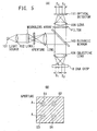
- FIG. 2 is a schematic block diagram showing an example of the conventional biochip reader described earlier.
- the numeral 1 indicates a light source for emitting excitation light, such as a laser light source
- the numeral 2 indicates a dichroic mirror
- the numeral 3 indicates an objective lens
- the numeral 4 indicates a DNA chip which is a biochip onto which multiple cells are arranged in arrays
- the numeral 5 indicates a filter
- the numeral 6 indicates a lens
- the numeral 7 indicates an optical detector, such as a photomultiplier tube.
- CL01 to CL03 are the aforementioned cells in which DNA segments, namely samples, of the same type are arranged.
- Light emitted from the light source 1 is reflected by the dichroic mirror 2 as excitation light and condensed onto cells on the DNA chip 4 through the objective lens 3.
- the excitation light is condensed onto the cell CL02.
- Fluorescent light produced by the excitation light in the cell CL02 becomes parallel light as it travels through the objective lens 3, and passes through the dichroic mirror 2. Fluorescent light that has passed through the dichroic mirror 2 travels through the filter 5 and is condensed onto the optical detector 7 by the lens 6.
- the DNA chip 4 is scanned by a drive means which is not shown in FIG. 2 .
- the DNA chip 4 is scanned in the direction indicated by MV01 in FIG. 2 so that the excitation light is irradiated at the remaining cells CL01 and CL03 on the DNA chip 4.
- Dust may deposit on the DNA chip 4, however, for such reasons as the mixing of foreign matter with a liquid in which the unknown DNA segment is hybridized or the way subsequent processes are carried out. If the dust is organic, the excitation light causes the dust to emit fluorescent light that is more intense than that emitted by a cell. This results in the problem that the fluorescent light serves as noise and therefore deteriorates the S/N ratio.
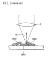
- FIG. 3 is an enlarged view of the cell CL02 shown in FIG. 2 .
- Members indicated by 3, 4 and CL02 are the same as those in FIG. 2 . If the DNA chip 4 is contaminated with dust particles marked DS01 and DS02 in FIG. 3 , fluorescent light indicated by LL11 is produced by the excitation light in addition to fluorescent light emitted from the cell CL02. This deteriorates the S/N ratio.
- a confocal optical system has been used with the conventional biochip reader to detect only the fluorescent light produced by cells by removing fluorescent light produced by dust.
- a DNA chip has been hermetically sealed to prevent it from being contaminated with dust.
- these measures have caused the problems not only of increased cost but also of insufficiently improved S/N ratio.
- the objective of the present invention is therefore to provide a biochip reader whose S/N ratio is superior and whose cost can be reduced.
- WO 99/23474 A discloses an optical array system and a reader for micro titer plates, wherein the optical system is made of lens arrays and normal lenses arranged to allow parallel reading of plural wells of a micro titer plate in absorption, fluorescence and luminescence.
- WO 94/27137 A discloses an apparatus and methods for evanescent light fluoroimmunoassays.
- the appratus employs a planar waveguide with an integral semi-cylindrical lens integrally attached to the waveguide adjacent a receiving edge of the wave guide for receiving light from a light source.
- Detection means are provided for simultaneously separately collecting a plurality of fluoreszent signals each corresponding to an individual one of a plurality of patches of immobilized capture molecules provided on one of the surfaces of the waveguide.
- the present invention provides a biochip reader, wherein light is irradiated at a biochip onto which multiple samples are arranged in spots or in linear arrays and image data according to the multiple samples is read using an optical detector.
- the biochip reader comprises means for arranging multiple pieces of spectroscopic information on the sample under analysis in spaces between the images of the aforementioned samples. According to the biochip reader configured in such a way as described above, it is possible to output pieces of spectroscopic information on the samples into spaces between the images of the samples and thereby realize simultaneous, multi-wavelength measurement easily. According to this configuration, it is also possible to acquire multi-wavelength information using a compact biochip reader.
- the biochip reader comprises a light source for emitting excitation light, a dichroic mirror for reflecting or transmitting the excitation light, an objective lens for condensing the excitation light reflected or transmitted by the dichroic mirror and projecting fluorescent light produced at the biochip onto the dichroic mirror, an optical detector for detecting the fluorescent light, and a lens for condensing the excitation light reflected or transmitted by the dichroic mirror onto the detector.
- the biochip is fabricated using a transparent substrate that can transmit both the excitation light and fluorescent light and the excitation light is irradiated from the side opposite to the side where the samples are arranged on the biochip. According to this configuration, it is possible to improve the S/N ratio of the biochip reader and reduce the cost thereof.
- FIG. 6 is a schematic block diagram showing one embodiment of a biochip reader in accordance with the present invention.
- the numeral 101 indicates a light source for emitting laser light
- the numeral 102 indicates a lens for making parallel the laser light emitted by the light source 101
- the numeral 103 indicates a dichroic mirror
- the numeral 106 indicates an objective lens
- the symbol S indicates a sample
- the symbol G indicates a grating
- the numeral 108 indicates a lens
- the numeral 109 indicates an optical detector.
- Excitation light emitted by the light source 101 is made parallel by the lens 102, is reflected by the dichroic mirror 103, is condensed through the objective lens 106, and is irradiated at the sample S. This irradiation causes the sample S to emit fluorescent light (whose wavelength differs from that of the excitation light). The fluorescent light then follows back the path that the excitation light followed, by passing through the objective lens 106 and reaching the dichroic mirror 103.
- the diffraction angle of the fluorescent light is relative to its wavelength.
- the fluorescent light thus diffracted by the grating G is condensed onto the optical detector 109 through the lens 108.
- the optical detector 109 a camera is used, for example.
- spectroscopic images with wavelengths of ⁇ 1 to ⁇ n are formed for these respective samples in spatially different positions on the optical detector 109, as shown in FIG. 8 .
- These spectroscopic images are spectroscopic information and can well be measured with a monochrome camera. As is evident from the figures, gaps between the spots are skillfully used in this example.
- the present invention is not limited to this sample arrangement.
- the invention can also be applied to fluorescence patterns of electrophoresis arranged in linear arrays.
- images shown in FIG. 9 are obtained. That is, spectroscopic images with wavelengths of ⁇ 1 to ⁇ n are formed for the electrophoresis pattern of each lane (along the longitudinal axis) in spatially different positions along the lateral axis.
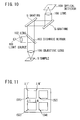
- FIG. 10 is a schematic block diagram showing another embodiment of the present invention.
- two gratings are arranged so that their directions of diffraction are at right angles to each other. According to this configuration, two-dimensional spectra are obtained as shown in FIG. 11 . If, for example, the spectral pattern is graduated in 100-nm increments laterally (X-axis direction) and in 10-nm increments longitudinally (Y-axis direction), it is possible to perform measurement with a wider dynamic range and higher precision.
- FIG. 12 shows an embodiment in which dichroic mirrors are used in place of the gratings. These dichroic mirrors are combinations of optical filters with optical shift means. As shown in FIG. 12 , dichroic mirrors (optical filters) 31, 32 and 33 with different transmission wavelengths are stacked on the optical axis. In this embodiment, the angle of each dichroic mirror is determined so that light is reflected by the dichroic mirror at the same angle as it diffracts at a grating (equivalent to the optical shift means).
- FIG. 13 is an embodiment in which a non-moving Fourier spectrometer 81, such as a Savart or a Michelson model, is used in place of the gratings or dichroic mirrors.
- images formed at the optical detector 109 are not spectra themselves but an image of interference fringes. Consequently, spectra can be obtained by using computation means (not shown in the figure) and submitting this image to a Fourier transform process.
- the measurement resolution can be further improved by using a confocal microscope or 2 photon microscope instead of a regular fluorescent substance or a camera.
- the quantitativeness of measurement is also improved because the slice effect of the confocal method makes it possible to always measure a constant volume of samples even if the thickness of each sample varies.
- the confocal microscope may be of the non-scanning type.
- a shield means such as slits. If the area of the shield means is greater than the area of a sample, dead spaces are produced in the imaging area of an optical detector. Conversely, if the area of the shield means is smaller than the area of the sample, dead spaces are produced in the area of the sample.
- an aperture A is optically aligned with the area of a sample S1 or with part of the sample S1, for example, as shown in FIG. 5 (A) and FIG. 5 (B) .
- This arrangement makes it possible to most effectively use both the area of the sample S1 and the imaging area of the optical detector. This arrangement is also effective for removing errors due to disorder in the edges of a sample.
- the shape of the aperture may not necessarily be circular; it may be rectangular instead.
- the aperture shown in FIG. 5 (A) or FIG. 5 (B) or the rectangular aperture described above may be used as a pinhole or slit for a non-scanning confocal microscope.
- This approach it is possible for even a small and inexpensive microscope to achieve the high resolution characteristic of confocal microscopes and the quantitativeness due to the slice effect.
- the detection means is not limited to the spectroscopy method shown in FIG. 6 , but may be a regular filter method.
- Luminous energy can be increased further by attaching a microlens array MA to the light-source side of an aperture AP.
- Use of the microlens array MA eliminates the need for the aperture AP since light beams are condensed onto the focal point of each microlens.
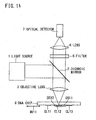
- FIG. 14 is a schematic block diagram showing one example of a biochip reader for explaining certain features of the present invention.
- members indicated by 1 to 3 and 5 to 7 are the same as those in FIG. 2
- the numeral 8 indicates a DNA chip using a plastic or glass substrate which allows excitation light or fluorescent light to pass through it.
- Members indicated by CL11 to CL13 are cells the same as those described earlier on which multiple samples of DNA segments of the same type are arranged.
- the symbols DS11 and DS12 indicate dust particles adhering to the cell CL12 on the DNA chip 8.
- the excitation light is irradiated at the cell CL12 through the transparent substrate of the DNA chip 8.
- Fluorescent light produced by the excitation light at the cell is made parallel through the objective lens 3, and passes through the dichroic mirror 2.
- the fluorescent light that has passed through the dichroic mirror 2 is condensed by a lens 6 onto the optical detector 7 through a filter 5.
- the fluorescent light produced by the excitation light at the cell passes through the DNA chip 8 and is output to the side opposite to the side where the cells are arranged.
- the DNA chip 8 is scanned by a drive means which is not shown in the figure.
- the DNA chip 8 is scanned in the direction indicated by MV11 in FIG. 14 so that the excitation light is irradiated at the remaining cells CL11 and CL13 on the DNA chip 8.
- Liquid in which unknown DNA segments are hybridized is flowed onto the side where the cells, such as the cell CL12, shown in FIG. 14 are arranged.
- the dust particles DS11 and DS12 adhere to the side of the substrate where the cells are arranged on the DNA chip 8.
- fluorescent light resulting from the dust particle and serving as a noise component can be reduced by irradiating the excitation light from the side opposite to the side where the cells are arranged on the DNA chip 8.
- the excitation light is irradiated at the neighbors of a boundary between the substrate of the DNA chip and a cell.
- biochips are, as the matter of course, not limited to a DNA chip only. They may be such chips as fabricated by arranging in arrays segments of ribonucleic acid (RNA), protein or sugar chain on a transparent substrate.
- RNA ribonucleic acid
- RNA segments undergo hybridization as with DNA segments, while protein segments and sugar chain segments are submitted to an antigen-antibody reaction.
- segments of known samples combine with segments of unknown samples marked with a fluorescent substance.
- FIG. 14 is of the non-immersion type, it may be of the immersion type, such as a water immersion or an oil immersion lens.
- FIG. 15 is a partially enlarged view of the cell CL12 shown in FIG. 14 when an immersion lens is used. Members indicated by 3, 8 and CL12 in FIG. 15 are the same as those in FIG. 14 .
- the symbol LQ11 indicates a fluid such as water or oil filled into the gap between the objective lens 3 and the DNA chip 8.
- the numerical aperture (NA) is improved, thereby improving the S/N ratio further, because of the refractive index of fluid, such as water or oil.
- the method in which beams of excitation light itself are scanned is more suitable than scanning the DNA chip 8 or the objective lens 3.
- FIG. 16 is a partially enlarged view of the cell CL12 shown in FIG. 14 when a solid immersion lens (SIL), which has the same effect as an immersion lens, is used.
- SIL solid immersion lens
- members indicated by 8 and CL12 are the same as those in FIG. 14
- the numeral 9 indicates an SIL.
- NA numerical aperture
- the numerical aperture (NA) is improved by the SIL, thereby improving the S/N ratio further.
- the substrate of a DNA chip 8 may be prepared by placing transparent electrodes made of an indium-tin oxide (ITO) film on a transparent substrate. Hybridization can be accelerated by applying a positive voltage to the electrodes because DNA is charged with negative electricity.
- ITO indium-tin oxide
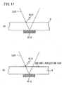
- An anti-reflection coating may be placed on the surface of the DNA chip 8's substrate opposite to the surface where cells are arranged.
- FIG. 17 is a schematic view showing comparison between DNA chips with and without an anti-reflection coating.
- FIG. 17 (A) members indicated by 8 and CL12 are the same as those in FIG. 14 , and the numeral 200 indicates an anti-reflection coating.
- the structure of the DNA chip 8 shown in FIG. 17 (A) is the same as the one shown in FIG. 14 .
- the anti-reflection coating 200 is formed on one side of the substrate of the DNA chip 8 opposite to the side where cells are arranged.
- the ratio of reflected light RL01 to incident light IL01 is approximately "4%".
- the ratio of reflected light RL11 to incident light IL11 can be reduced to as small as approximately "0.5%". Consequently, the luminous energy of excitation light irradiated at cells on the DNA chip 8 increases, improving the S/N ratio.
- the side of the substrate of the DNA chip 8 where cells are arranged may be in the state of dryness. It is also possible to leave that side of the substrate wetted with hybridization liquid.
- a laser light source has been mentioned earlier as an example of the source of excitation light
- a non-laser light source such as an LED lamp, xenon lamp, halogen lamp or any other white light source, may be used instead.
- the present invention offers the following advantages.
- their optical detector may be one of the means shown in FIG. 6 , FIG. 10 , FIG. 12 and FIG. 13 .
Landscapes
- Health & Medical Sciences (AREA)
- Life Sciences & Earth Sciences (AREA)
- Chemical & Material Sciences (AREA)
- Immunology (AREA)
- Physics & Mathematics (AREA)
- General Physics & Mathematics (AREA)
- Biochemistry (AREA)
- General Health & Medical Sciences (AREA)
- Analytical Chemistry (AREA)
- Pathology (AREA)
- Nuclear Medicine, Radiotherapy & Molecular Imaging (AREA)
- Molecular Biology (AREA)
- Chemical Kinetics & Catalysis (AREA)
- Electrochemistry (AREA)
- Optics & Photonics (AREA)
- Investigating, Analyzing Materials By Fluorescence Or Luminescence (AREA)
Claims (8)
- Ein Biochip-Lesegerät zum Lesen von Bilddaten gemäß mehreren Proben (S), die in Punkten oder Arrays auf einem Biochip angeordnet sind, unter Verwendung eines optischen Detektors (109) durch Aufstrahlen von Licht auf den Biochip, wobei das Biochip-Lesegerät umfaßt:ein Mittel (G;31-33;81) zum Anordnen von mehreren Stücken von spektroskopischer Information auf den Proben (S) unter Analyse in Räumen zwischen Bildern,dadurch gekennzeichnet, dassdas Mittel (G;31-33;81) so konfiguriert ist, dass die spektroskopische Information auf dem optischen Detektor (109) in einer zweidimensionalen Weise entwickelt wird, wenn die Proben (S) in Punkten angeordnet sind.
- Das Biochip-Lesegerät gemäß Anspruch 1, wobei das Mittel ein Gitter (G), eine Kombination eines optischen Filters und eines optischen Schiebemittels ("optical shift means") (31-33) oder ein Fourier-Spektrometer (81) umfaßt, die bzw. das zwischen den Proben (S) und dem optischen Detektor (109) angeordnet ist.
- Das Biochip-Lesegerät gemäß Anspruch 1, wobei das Mittel ein konfokales Abtastmikroskop ("scanning confocal microscope"), ein nicht-abtastendes konfokales Mikroskop ("non-scanning confocal microscope") oder ein Doppelgitter-Anregungsmikroskop ("dual-grating excitation microscope") ist.
- Das Biochip-Lesegerät gemäß Anspruch 1 oder 2, ferner mit Mitteln zum Trennen von Signalen der spektroskopischen Information von Rauschen unter Verwendung bekannter Spektren und einem Regressionsverfahren.
- Das Biochip-Lesegerät gemäß Anspruch 1 oder 2, wobei eine Apertur (A) zum Begrenzen einer Fläche der Spektroskopie mit der Position jeder Probe (S) oder mit einem Teil jeder Probe (S) ausgerichtet ist.
- Das Biochip-Lesegerät gemäß Anspruch 5, wobei eine Mikrolinsenanordnung ("microlens array") (MA) an der Lichtquellenseite der Apertur angebracht ist.
- Das Biochip-Lesegerät gemäß Anspruch 1 oder 2, ferner mit:einer Lichtquelle (101) zum Emittieren von Anregungslicht,einem dichroitischen Spiegel (103) zum Reflektieren des Anregungslichts oder zum Passierenlassen des Anregungslichts,einer Objektivlinse (106) zum Kondensieren von Licht, das von dem dichroitischen Spiegel (103) reflektiert wurde oder diesen passiert hat auf den Biochip und zum Projizieren von fluoreszierendem Licht, das an dem Biochip erzeugt wurde, auf den dichroitischen Spiegel (103),einem optischen Detektor (109) zum Erfassen des fluoreszierenden Lichts, undeiner Linse (108) zum Kondensieren des fluoreszierenden Lichts, das durch den dichroitischen Spiegel (103) reflektiert wurde und diesen passiert hat, auf den optischen Detektor (109).
- Das Biochip-Lesegerät gemäß einem der Ansprüche 1 bis 7, wobei der Biochip unter Verwendung eines transparenten Substrats, das den Durchgang von Anregungs- und von fluoreszierendem Licht erlaubt, konfiguriert ist, und das Anregungslicht von einer Seite des Biochips gegenüber der Seite, an der die Proben angeordnet sind, aufgestrahlt ist bzw. wird.
Priority Applications (1)
| Application Number | Priority Date | Filing Date | Title |
|---|---|---|---|
| EP08160013A EP1983331B1 (de) | 1999-05-28 | 2000-05-08 | Optische Anordnung zur Auswertung eines Biochips |
Applications Claiming Priority (6)
| Application Number | Priority Date | Filing Date | Title |
|---|---|---|---|
| JP14939999 | 1999-05-28 | ||
| JP14939999A JP3689901B2 (ja) | 1999-05-28 | 1999-05-28 | バイオチップ読取装置 |
| JP14940099A JP3695631B2 (ja) | 1999-05-28 | 1999-05-28 | 電気泳動装置 |
| JP14940099 | 1999-05-28 | ||
| JP2000007724 | 2000-01-17 | ||
| JP2000007724A JP3859050B2 (ja) | 2000-01-17 | 2000-01-17 | バイオチップ読み取り装置 |
Related Child Applications (2)
| Application Number | Title | Priority Date | Filing Date |
|---|---|---|---|
| EP08160013A Division EP1983331B1 (de) | 1999-05-28 | 2000-05-08 | Optische Anordnung zur Auswertung eines Biochips |
| EP08160013.2 Division-Into | 2008-07-09 |
Publications (3)
| Publication Number | Publication Date |
|---|---|
| EP1055925A2 EP1055925A2 (de) | 2000-11-29 |
| EP1055925A3 EP1055925A3 (de) | 2004-05-12 |
| EP1055925B1 true EP1055925B1 (de) | 2010-09-08 |
Family
ID=27319743
Family Applications (2)
| Application Number | Title | Priority Date | Filing Date |
|---|---|---|---|
| EP08160013A Expired - Lifetime EP1983331B1 (de) | 1999-05-28 | 2000-05-08 | Optische Anordnung zur Auswertung eines Biochips |
| EP00109722A Expired - Lifetime EP1055925B1 (de) | 1999-05-28 | 2000-05-08 | Biochip-Lesegerät |
Family Applications Before (1)
| Application Number | Title | Priority Date | Filing Date |
|---|---|---|---|
| EP08160013A Expired - Lifetime EP1983331B1 (de) | 1999-05-28 | 2000-05-08 | Optische Anordnung zur Auswertung eines Biochips |
Country Status (3)
| Country | Link |
|---|---|
| US (2) | US20040182710A1 (de) |
| EP (2) | EP1983331B1 (de) |
| DE (2) | DE1055925T1 (de) |
Cited By (2)
| Publication number | Priority date | Publication date | Assignee | Title |
|---|---|---|---|---|
| CN104568893A (zh) * | 2015-01-24 | 2015-04-29 | 北京中拓机械集团有限责任公司 | 半导体晶片的高速荧光光谱检测装置 |
| CN106841137A (zh) * | 2017-01-10 | 2017-06-13 | 清华大学 | 单曝光下多色荧光成像的方法和系统 |
Families Citing this family (36)
| Publication number | Priority date | Publication date | Assignee | Title |
|---|---|---|---|---|
| US20040112535A1 (en) * | 2000-04-13 | 2004-06-17 | Olympus Optical Co., Ltd. | Focus detecting device |
| JP3741051B2 (ja) * | 2001-05-10 | 2006-02-01 | 横河電機株式会社 | バイオチップ読取装置 |
| CN100404692C (zh) | 2001-05-11 | 2008-07-23 | 松下电器产业株式会社 | 生物分子基底,使用它的检验和诊断方法及装置 |
| DE10131687A1 (de) * | 2001-06-29 | 2003-01-16 | Eppendorf Ag | Vorrichtung zur Durchführung von Nukleinsäure-Amplifikationsreaktionen bei gleichzeitiger Verfolgung der Bildung von Amplifikationsprodukten |
| US20030031596A1 (en) * | 2001-08-09 | 2003-02-13 | Yokogawa Electric Corporation | Biochip reader and fluorometric imaging apparatus |
| DE102004015488B4 (de) * | 2004-03-26 | 2008-01-31 | Lavision Biotec Gmbh | Verfahren zum Auslesen durch streifenweises Abtasten von flächigen Objekten mit Substanzen, die Fluoreszenzstrahlung abgeben |
| JP4701739B2 (ja) * | 2005-02-17 | 2011-06-15 | パナソニック株式会社 | 蛍光測定装置 |
| US7663750B2 (en) * | 2005-06-30 | 2010-02-16 | Applied Biosystems, Llc | Two-dimensional spectral imaging system |
| US7817273B2 (en) * | 2005-06-30 | 2010-10-19 | Life Technologies Corporation | Two-dimensional spectral imaging system |
| US7805081B2 (en) * | 2005-08-11 | 2010-09-28 | Pacific Biosciences Of California, Inc. | Methods and systems for monitoring multiple optical signals from a single source |
| US7518728B2 (en) * | 2005-09-30 | 2009-04-14 | Intel Corporation | Method and instrument for collecting fourier transform (FT) Raman spectra for imaging applications |
| US20070131870A1 (en) * | 2005-12-12 | 2007-06-14 | Combisep | Multiplexed CE fluorescence system |
| US7692783B2 (en) * | 2006-02-13 | 2010-04-06 | Pacific Biosciences Of California | Methods and systems for simultaneous real-time monitoring of optical signals from multiple sources |
| SE529711C2 (sv) * | 2006-03-22 | 2007-11-06 | Aamic Ab | Fluorescensläsare |
| US20080277595A1 (en) * | 2007-05-10 | 2008-11-13 | Pacific Biosciences Of California, Inc. | Highly multiplexed confocal detection systems and methods of using same |
| US20100167413A1 (en) * | 2007-05-10 | 2010-07-01 | Paul Lundquist | Methods and systems for analyzing fluorescent materials with reduced autofluorescence |
| US20090262332A1 (en) * | 2008-04-18 | 2009-10-22 | Microvast, Inc. | High-throughput spectral imaging and spectroscopy apparatus and methods |
| EP2163885A1 (de) * | 2008-06-24 | 2010-03-17 | Koninklijke Philips Electronics N.V. | System und Verfahren zur Mikroarraycharakterisierung |
| CN102077080B (zh) * | 2008-06-24 | 2014-06-18 | 皇家飞利浦电子股份有限公司 | 微阵列表征系统和方法 |
| US8275226B2 (en) | 2008-12-09 | 2012-09-25 | Spectral Applied Research Ltd. | Multi-mode fiber optically coupling a radiation source module to a multi-focal confocal microscope |
| WO2010121643A1 (en) * | 2009-04-20 | 2010-10-28 | Agilent Technologies, Inc. | Identifying calibration markers in multiple detection channels |
| US8357281B2 (en) * | 2009-09-21 | 2013-01-22 | Advanced Analytical Technologies, Inc. | Multi-wavelength fluorescence detection system for multiplexed capillary electrophoresis |
| US8670178B2 (en) * | 2009-12-08 | 2014-03-11 | Spectral Applied Research Inc. | Imaging distal end of multimode fiber |
| US8830451B1 (en) | 2010-05-07 | 2014-09-09 | Stc.Unm | Multinode acoustic focusing for parallel flow cytometry analysis applications |
| US9274042B2 (en) | 2010-05-07 | 2016-03-01 | Stc.Unm | Spatially correlated light collection from multiple sample streams excited with a line focused light source |
| US9074977B2 (en) | 2010-05-07 | 2015-07-07 | Stc.Unm | Multinode acoustic focusing for parallel flow cytometry analysis applications |
| DE102011083718A1 (de) * | 2011-09-29 | 2013-04-04 | Siemens Aktiengesellschaft | Konfokales Spektrometer und Verfahren zur Bildgebung in einem konfokalen Spektrometer |
| EP2864762A4 (de) * | 2012-06-21 | 2016-01-20 | Stc Unm | Räumlich korrelierte lichtsammlung aus mehreren mit einer leitungsfokussierten lichtquelle angeregten probenströmen |
| CN102818886A (zh) * | 2012-08-28 | 2012-12-12 | 天津市先石光学技术有限公司 | 一种小剂量均相激发光免疫检测仪 |
| US9581550B2 (en) * | 2013-05-31 | 2017-02-28 | Pacific Biosciences Of California | Analytical devices having compact lens train arrays |
| DE102014111167A1 (de) * | 2014-08-06 | 2016-02-11 | Carl Zeiss Microscopy Gmbh | Hochauflösende Scanning-Mikroskopie mit der Unterscheidung mindestens zweier Wellenlängenbereiche |
| CN105424698B (zh) * | 2015-11-25 | 2018-05-15 | 江苏三联生物工程有限公司 | 一种带抓手功能的生物芯片阅读仪 |
| US10883820B2 (en) | 2017-11-13 | 2021-01-05 | Taiwan Semiconductor Manufacturing Co., Ltd. | Apparatus and method for metrology |
| WO2019136579A1 (zh) * | 2018-01-09 | 2019-07-18 | 深圳达闼科技控股有限公司 | 微型光谱检测设备 |
| WO2021049109A1 (ja) * | 2019-09-11 | 2021-03-18 | パナソニックIpマネジメント株式会社 | 水分検知装置 |
| US10895727B1 (en) * | 2019-10-19 | 2021-01-19 | SequLITE Genomics US, Inc. | Microscope for locating structures on the inner surface of a fluidic channel |
Family Cites Families (22)
| Publication number | Priority date | Publication date | Assignee | Title |
|---|---|---|---|---|
| US4790919A (en) * | 1984-06-28 | 1988-12-13 | E. I. Du Pont De Nemours And Company | Process for preparation of electrophoresis gel material |
| EP0217619A3 (de) | 1985-09-26 | 1989-01-25 | Molecular Devices Corporation | Verfahren und Vorrichtung zur Abbildung von optisch nachprüfbaren Reaktionsversuchen |
| US5274240A (en) * | 1990-01-12 | 1993-12-28 | The Regents Of The University Of California | Capillary array confocal fluorescence scanner and method |
| US5038352A (en) * | 1990-11-13 | 1991-08-06 | International Business Machines Incorporation | Laser system and method using a nonlinear crystal resonator |
| US5324633A (en) * | 1991-11-22 | 1994-06-28 | Affymax Technologies N.V. | Method and apparatus for measuring binding affinity |
| US5422712A (en) * | 1992-04-01 | 1995-06-06 | Toa Medical Electronics Co., Ltd. | Apparatus for measuring fluorescent spectra of particles in a flow |
| CA2162996C (en) * | 1993-05-18 | 2008-02-05 | James N. Herron | Apparatus and methods for multianalyte homogeneous fluoroimmunoassays |
| US5538613A (en) * | 1993-10-26 | 1996-07-23 | Genesys Technologies, Inc. | Electrophoresis analyzer |
| US5578832A (en) * | 1994-09-02 | 1996-11-26 | Affymetrix, Inc. | Method and apparatus for imaging a sample on a device |
| DE19510102C1 (de) * | 1995-03-20 | 1996-10-02 | Rainer Dr Uhl | Konfokales Fluoreszenzmikroskop |
| US5859700A (en) * | 1995-11-22 | 1999-01-12 | Kairos Scientific, Inc. | High resolution imaging microscope (HIRIM) and uses thereof |
| US5871628A (en) * | 1996-08-22 | 1999-02-16 | The University Of Texas System | Automatic sequencer/genotyper having extended spectral response |
| ATE335845T1 (de) * | 1997-05-16 | 2006-09-15 | Exact Sciences Corp | Elektrophoretische analyse von molekülen mit immobilisierten sonden |
| WO1998058370A1 (en) * | 1997-06-16 | 1998-12-23 | Digital Papyrus Corporation | Planar proximity lens element and disk drive using same |
| DE19748211A1 (de) * | 1997-10-31 | 1999-05-06 | Zeiss Carl Fa | Optisches Array-System und Reader für Mikrotiterplatten |
| US6100535A (en) * | 1998-01-29 | 2000-08-08 | The Regents Of The University Of California | Rotary confocal scanner for detection of capillary arrays |
| US6100541A (en) * | 1998-02-24 | 2000-08-08 | Caliper Technologies Corporation | Microfluidic devices and systems incorporating integrated optical elements |
| US6406921B1 (en) * | 1998-07-14 | 2002-06-18 | Zyomyx, Incorporated | Protein arrays for high-throughput screening |
| US6603537B1 (en) * | 1998-08-21 | 2003-08-05 | Surromed, Inc. | Optical architectures for microvolume laser-scanning cytometers |
| US6642062B2 (en) * | 1998-09-03 | 2003-11-04 | Trellis Bioinformatics, Inc. | Multihued labels |
| JP2000147421A (ja) * | 1998-11-17 | 2000-05-26 | Yokogawa Electric Corp | 共焦点光スキャナ |
| AU2001249237A1 (en) * | 2000-03-16 | 2001-09-24 | Spectrumedix Corporation | Multi-wavelength array reader for biological assay |
-
2000
- 2000-05-08 EP EP08160013A patent/EP1983331B1/de not_active Expired - Lifetime
- 2000-05-08 DE DE1055925T patent/DE1055925T1/de active Pending
- 2000-05-08 EP EP00109722A patent/EP1055925B1/de not_active Expired - Lifetime
- 2000-05-08 DE DE60044923T patent/DE60044923D1/de not_active Expired - Lifetime
-
2004
- 2004-01-30 US US10/769,017 patent/US20040182710A1/en not_active Abandoned
- 2004-01-30 US US10/768,632 patent/US20040184960A1/en not_active Abandoned
Cited By (2)
| Publication number | Priority date | Publication date | Assignee | Title |
|---|---|---|---|---|
| CN104568893A (zh) * | 2015-01-24 | 2015-04-29 | 北京中拓机械集团有限责任公司 | 半导体晶片的高速荧光光谱检测装置 |
| CN106841137A (zh) * | 2017-01-10 | 2017-06-13 | 清华大学 | 单曝光下多色荧光成像的方法和系统 |
Also Published As
| Publication number | Publication date |
|---|---|
| DE60044923D1 (de) | 2010-10-21 |
| EP1983331B1 (de) | 2011-07-13 |
| US20040184960A1 (en) | 2004-09-23 |
| EP1055925A3 (de) | 2004-05-12 |
| DE1055925T1 (de) | 2001-06-07 |
| EP1983331A3 (de) | 2008-11-05 |
| EP1055925A2 (de) | 2000-11-29 |
| EP1983331A2 (de) | 2008-10-22 |
| US20040182710A1 (en) | 2004-09-23 |
Similar Documents
| Publication | Publication Date | Title |
|---|---|---|
| EP1055925B1 (de) | Biochip-Lesegerät | |
| US8264680B2 (en) | Biochip reader and electrophoresis system | |
| US8149399B2 (en) | Methods and systems for simultaneous real-time monitoring of optical signals from multiple sources | |
| AU2007215173B2 (en) | Methods and systems for simultaneous real-time monitoring of optical signals from multiple sources | |
| US6704104B2 (en) | Multi-wavelength array reader for biological assay | |
| US6654119B1 (en) | Scanning spectrophotometer for high throughput fluroescence detection | |
| KR100590548B1 (ko) | 광검출 장치 | |
| WO1999058963A1 (en) | Sensing unit provided with separated detection light guiding | |
| WO2003021209A1 (en) | System for high throughput analysis | |
| JP2001311690A (ja) | バイオチップ読取装置及び電気泳動装置 | |
| KR20030079577A (ko) | 레이저 유발 표면형광 검출 장치 | |
| JP2011002398A (ja) | 分光イメージング装置 | |
| RU2679605C2 (ru) | Флуориметрический анализатор биологических микрочипов | |
| CN119053846A (zh) | 宽谱分析系统 | |
| AU2011202922A1 (en) | Methods and systems for simultaneous real-time monitoring of optical signals from multiple sources |
Legal Events
| Date | Code | Title | Description |
|---|---|---|---|
| PUAI | Public reference made under article 153(3) epc to a published international application that has entered the european phase |
Free format text: ORIGINAL CODE: 0009012 |
|
| AK | Designated contracting states |
Kind code of ref document: A2 Designated state(s): AT BE CH CY DE DK ES FI FR GB GR IE IT LI LU MC NL PT SE |
|
| AX | Request for extension of the european patent |
Free format text: AL;LT;LV;MK;RO;SI |
|
| TCNL | Nl: translation of patent claims filed | ||
| DET | De: translation of patent claims | ||
| PUAL | Search report despatched |
Free format text: ORIGINAL CODE: 0009013 |
|
| AK | Designated contracting states |
Kind code of ref document: A3 Designated state(s): AT BE CH CY DE DK ES FI FR GB GR IE IT LI LU MC NL PT SE |
|
| AX | Request for extension of the european patent |
Extension state: AL LT LV MK RO SI |
|
| 17P | Request for examination filed |
Effective date: 20040727 |
|
| AKX | Designation fees paid |
Designated state(s): DE GB NL |
|
| 17Q | First examination report despatched |
Effective date: 20080125 |
|
| GRAP | Despatch of communication of intention to grant a patent |
Free format text: ORIGINAL CODE: EPIDOSNIGR1 |
|
| RTI1 | Title (correction) |
Free format text: BIOCHIP READER |
|
| GRAS | Grant fee paid |
Free format text: ORIGINAL CODE: EPIDOSNIGR3 |
|
| GRAA | (expected) grant |
Free format text: ORIGINAL CODE: 0009210 |
|
| AK | Designated contracting states |
Kind code of ref document: B1 Designated state(s): DE GB NL |
|
| REG | Reference to a national code |
Ref country code: GB Ref legal event code: FG4D |
|
| REF | Corresponds to: |
Ref document number: 60044923 Country of ref document: DE Date of ref document: 20101021 Kind code of ref document: P |
|
| REG | Reference to a national code |
Ref country code: NL Ref legal event code: T3 |
|
| PLBE | No opposition filed within time limit |
Free format text: ORIGINAL CODE: 0009261 |
|
| STAA | Information on the status of an ep patent application or granted ep patent |
Free format text: STATUS: NO OPPOSITION FILED WITHIN TIME LIMIT |
|
| 26N | No opposition filed |
Effective date: 20110609 |
|
| REG | Reference to a national code |
Ref country code: DE Ref legal event code: R097 Ref document number: 60044923 Country of ref document: DE Effective date: 20110609 |
|
| PGFP | Annual fee paid to national office [announced via postgrant information from national office to epo] |
Ref country code: NL Payment date: 20140410 Year of fee payment: 15 |
|
| REG | Reference to a national code |
Ref country code: NL Ref legal event code: MM Effective date: 20150601 |
|
| PG25 | Lapsed in a contracting state [announced via postgrant information from national office to epo] |
Ref country code: NL Free format text: LAPSE BECAUSE OF NON-PAYMENT OF DUE FEES Effective date: 20150601 |
|
| PGFP | Annual fee paid to national office [announced via postgrant information from national office to epo] |
Ref country code: GB Payment date: 20160504 Year of fee payment: 17 Ref country code: DE Payment date: 20160504 Year of fee payment: 17 |
|
| REG | Reference to a national code |
Ref country code: DE Ref legal event code: R119 Ref document number: 60044923 Country of ref document: DE |
|
| GBPC | Gb: european patent ceased through non-payment of renewal fee |
Effective date: 20170508 |
|
| PG25 | Lapsed in a contracting state [announced via postgrant information from national office to epo] |
Ref country code: GB Free format text: LAPSE BECAUSE OF NON-PAYMENT OF DUE FEES Effective date: 20170508 Ref country code: DE Free format text: LAPSE BECAUSE OF NON-PAYMENT OF DUE FEES Effective date: 20171201 |