EP1056057A1 - Dispositif et procédé pour l'identification d'objets transmettant la lumière - Google Patents
Dispositif et procédé pour l'identification d'objets transmettant la lumière Download PDFInfo
- Publication number
- EP1056057A1 EP1056057A1 EP00110290A EP00110290A EP1056057A1 EP 1056057 A1 EP1056057 A1 EP 1056057A1 EP 00110290 A EP00110290 A EP 00110290A EP 00110290 A EP00110290 A EP 00110290A EP 1056057 A1 EP1056057 A1 EP 1056057A1
- Authority
- EP
- European Patent Office
- Prior art keywords
- light
- emitting
- identification target
- light source
- adjustment
- Prior art date
- Legal status (The legal status is an assumption and is not a legal conclusion. Google has not performed a legal analysis and makes no representation as to the accuracy of the status listed.)
- Withdrawn
Links
- 238000000034 method Methods 0.000 title claims description 26
- 238000001514 detection method Methods 0.000 claims abstract description 118
- 238000005070 sampling Methods 0.000 claims abstract description 31
- 239000002131 composite material Substances 0.000 claims description 9
- 238000003780 insertion Methods 0.000 claims description 6
- 230000037431 insertion Effects 0.000 claims description 6
- 230000006866 deterioration Effects 0.000 abstract description 6
- 238000012545 processing Methods 0.000 description 31
- 238000006243 chemical reaction Methods 0.000 description 21
- 238000012790 confirmation Methods 0.000 description 8
- 230000007423 decrease Effects 0.000 description 7
- 238000010586 diagram Methods 0.000 description 5
- 230000007246 mechanism Effects 0.000 description 5
- 238000002360 preparation method Methods 0.000 description 4
- 238000002834 transmittance Methods 0.000 description 4
- 239000003086 colorant Substances 0.000 description 3
- 239000000470 constituent Substances 0.000 description 3
- 101150051783 SWT1 gene Proteins 0.000 description 2
- 230000004397 blinking Effects 0.000 description 2
- 238000009434 installation Methods 0.000 description 2
- 101150002135 SDC1 gene Proteins 0.000 description 1
- 230000003247 decreasing effect Effects 0.000 description 1
- 238000012850 discrimination method Methods 0.000 description 1
- 230000000694 effects Effects 0.000 description 1
- 230000007613 environmental effect Effects 0.000 description 1
- 238000011156 evaluation Methods 0.000 description 1
- 230000001747 exhibiting effect Effects 0.000 description 1
- 230000002401 inhibitory effect Effects 0.000 description 1
- 239000003550 marker Substances 0.000 description 1
- 230000010355 oscillation Effects 0.000 description 1
- 230000035945 sensitivity Effects 0.000 description 1
Images


Classifications
-
- G—PHYSICS
- G07—CHECKING-DEVICES
- G07D—HANDLING OF COINS OR VALUABLE PAPERS, e.g. TESTING, SORTING BY DENOMINATIONS, COUNTING, DISPENSING, CHANGING OR DEPOSITING
- G07D7/00—Testing specially adapted to determine the identity or genuineness of valuable papers or for segregating those which are unacceptable, e.g. banknotes that are alien to a currency
- G07D7/06—Testing specially adapted to determine the identity or genuineness of valuable papers or for segregating those which are unacceptable, e.g. banknotes that are alien to a currency using wave or particle radiation
- G07D7/12—Visible light, infrared or ultraviolet radiation
Definitions
- the present invention relates to a light-transmitting object identifying apparatus and method which can easily authenticate a light-transmitting object.
- vending machines allow the use of bills, specific prepaid cards, and the like in addition to coins.
- Vending machines are installed in various places, and hence operate in various operation conditions. These machines are therefore required to exhibit satisfactory performance in every operation environment. This applies to mechanisms for authenticating coins, bills, and the like.
- the authenticity of a coin can be checked by examining its weight and shape, and hence a coin identifying mechanism can be mechanically formed.
- a light source and a light-receiving element are spaced apart from each other by a predetermined distance, and a bill is conveyed between them to detect a light and dark pattern unique to the light source. The detected pattern is then compared with a reference light and dark pattern held in advance, thereby authenticating the bill.
- a color sensor may be used.
- a color sensor is expensive and demands complicated signal processing, and hence cannot be used for a vending machine or the like which must meet a requirement for low cost as an absolute necessity.
- a white light source incandescent lamp
- the white light source has a short service life, and burns out in a short period of time when the ambient temperature becomes high as in a case wherein the machine is installed on a road under the hot sun. In such a case, even if a bill is inserted into the vending machine, the bill is determined as a counterfeit and rejected.
- the color appearance of a bill may be determined by using, for example, two light-emitting diodes for emitting light beams having different wavelengths as light sources and receiving the light beams from the light-emitting diodes with one light-receiving element.
- Light-emitting diodes vary in luminous efficacy. For this reason, the driving currents to the light-emitting diodes must be adjusted to equalize the performance ratios.
- an error signal is output in either of the two cases, i.e., a case wherein the output of the green light-emitting diode becomes equal to or higher than a reference level (the color of the bill is offset to green to some extent) and a case wherein the output of the red light-receiving element become equal to or higher than a reference level (the color of the bill is offset to red to some extent).
- Japanese Patent Laid-Open No. 54-066894 is, however, based on the assumption that "when the color of a bill does not shift (offset) to red or green, the amount of light received by the light-receiving element, i.e., the output, is at zero level as in the case of the absence of a bill".
- an error can only be determined when the color of the bill is offset to green or red to some extent.
- Some effect can be expected from this technique when a bill is printed in a specific color. If, however, bills are printed in full color as in Japan, it is almost impossible to authenticate bills by using the above technique.
- the service life of a light-emitting diode is inversely proportional to the emission time to a certain degree. If, therefore, the emission time of the light-emitting diode is too long, the diode deteriorates, resulting in a deterioration in identification performance. This is the problem that must be overcome by all means. That is, a deterioration in light-emitting diode needs to be suppressed.
- the present invention has been made to solve the above problems, and has as its object to provide a light-transmitting object identifying apparatus which can automatically solve problems associated with variations in performance of each constituent members of a mechanism for detecting an identification object, changes in performance over time, and changes in performance due to environments with a simple arrangement, can be easily manufactured and adjusted, and has high reliability.
- Fig. 1 shows the arrangement of a negotiable instrument identifying apparatus according to an embodiment of the present invention.
- Fig. 2 shows the detailed circuit arrangement of a light source B intensity changing/driving circuit as an automatic light source emission intensity adjusting circuit in Fig. 1.
- Fig. 3 shows the detailed circuit arrangement of a light source A driving circuit in Fig. 1.
- Fig. 4 shows the arrangement of a light source emission changing/driving circuit in a case wherein the light sources A and B are formed by using cathode common two-color LEDs.
- reference numeral 10 denotes a control unit for controlling the overall negotiable instrument identifying apparatus of this embodiment.
- the control unit 10 is comprised of a CPU 11 for performing various control operations in accordance with control procedures that are stored in, for example, a memory 12 and indicated by the flow charts to be described later, the memory 12 storing control programs for the CPU 11 and the like, a timer 13 for performing time control, an A/D converter 14 for converting an input analog signal into a corresponding digital signal, and a sampling circuit 15 for sampling an analog signal input through an input port.
- the CPU 11 outputs light source control data DD2 as light source control signals (Sa, Sb, Fb, and T) upon detection of a first half end signal UD1 from the timer 13, and outputs DD1 upon detection of UD2.
- the CPU 11 controls the sampling circuit 15 and A/D converter 14 to start A/D conversion.
- Reference numeral 21 denotes a light source A driving circuit for performing blink control on the light source A in accordance with a light source A blink signal Sa; and 22, a light source B intensity changing/driving circuit serving as an automatic emission intensity adjusting circuit for the light source B, which performs blink control on the light source B in accordance with a light source B blink signal Sb from the control unit 10, adjusts the emission intensity of the light source B in accordance with a light intensity adjustment signal T, and holds an adjusted state by stopping light intensity adjustment when a light intensity fixing signal Fb is output.
- Reference numeral 23 denotes a light source A/light source B capable of emitting light beams having different wavelengths.
- the light source A and light source B may be separate light-emitting elements, or may be a composite light source formed by integrating two light sources.
- Reference numeral 24 denotes a photoelectric converter for receiving light from the light source A/light source B 23 or light transmitted through an identification target 100, converting the received light into an electrical signal corresponding to the amount of light received, and outputting the signal, and it can be formed by using photodiode and the like.
- Reference numeral 25 denotes a log amplifier for amplifying the electrical signal from the photoelectric converter 24.
- a light-reception signal value from the photoelectric converter 24 is amplified by the log amplifier 25 for the following reason.
- a linear amplifier an output from the linear amplifier always contains absolute value components of emission intensity.
- offsets associated with absolute value components of emission intensity e.g., variations in the distance between the light source and the photoelectric converter, emission intensity, light-reception intensity, and the like, temperature characteristics, deterioration, and the like, cannot be basically removed.
- a log amplifier when a log amplifier is used, an output associated with only the properties of an identification target can be obtained.
- Is cancellation and the like unique to log amplifiers need not be performed, and the arrangement of a log amplifier itself can be simplified.
- Reference numeral 26 denotes a high-pass filter for removing components having frequencies less than the light source driving frequency (DC components and fluctuation components associated with brightness which are produced between the DC components and the light source driving frequency) from a detection electrical signal from the log amplifier 25; and 27, an amplifier circuit for superimposing a DC voltage V1 as a reference on the output from the high-pass filter 26, and outputting the resultant voltage.
- DC components and fluctuation components associated with brightness which are produced between the DC components and the light source driving frequency
- Reference numeral 31 denotes an interruption detection circuit for detecting an identification target.
- the interruption detection circuit 31 drives sensors, wave-shapes detection signals, and outputs the resultant signals to the control unit 10.
- the control unit 10 detects the position of the identification target 100 on the basis of detection signals Rck from identification target sensors 32, 33, and 34 and rotation sensor (Pr) 35.
- the input sensor (Pi) 32 detects the insertion of the identification target 100.
- the identification start sensor (Ps) 33 detects a reference for the position of the identification target 100 and also detects that the identification target 100 reaches the installation position (detection area) of the light source 23 and photoelectric converter 24.
- the pass sensor 34 detects that the identification target 100 passes through the installation position of the light source 23 and photoelectric converter 24 and moves outside the detection area.
- the rotation sensor (pr) 35 detects the rotation amount of a convey motor 41 (the convey amount of the identification target 100).
- the rotation sensor (pr) 35 detects pulses Rck for the rotation amount of the convey motor 41.
- Reference numeral 37 denotes a driving circuit for the convey motor 41.
- the driving circuit 37 drives the convey motor 41 in accordance with a motor switch signal Ms from the CPU 11 of the control unit 10.
- the convey motor 41 conveys the identification target 100.
- the identification target 100 includes an arbitrary object through which light is partly transmitted.
- a convey unit is designed for a sheet-like object as a target.
- an identification target having an arbitrary shape can identified by only changing the structure of the convey unit.
- control unit 10 is formed by using, for example, a one-chip microcomputer, which is connected to an external unit through an I/O port to simplify the hardware arrangement. If the control unit is designed to directly A/D-convert a sampled value of an AC output signal and load it as data into an identifying unit formed by the CPU 11, in particular, the circuit can be simplified.
- the control unit 10 in this embodiment performs authentication as follows.
- the photoelectric converter 24 is adjusted in advance such that the same output signal is obtained with respect to the light sources A and B that emit light beams having different wavelengths. Furthermore, the output signal of photoelectric converter 24 is adjusted by the light intensity of the light source B.
- the output difference between detection signals based on light beams transmitted through the identification target in this state is detected as an output from the high-pass filter 26.
- the sampling circuit 15 then samples a signal proportional to the difference in output between the detection values based on the light sources A and B, which is based on this output difference. Authentication is performed on the basis of the sampled value.
- the light source A blink signal Sa and light source B blink signal Sb are used to control this alternate emission.
- the light intensity adjustment signal T is used to adjust each emission intensity. When the identification target reaches a recognition area, the above adjustment is not performed, and light intensity is fixed.
- the light intensity fixing signal Fb is a control signal for this operation.
- a deterioration in the light sources is suppressed by periodically setting an interval during which only emission is stopped while the adjusted level is held in the absence of an identification target, instead of continuing adjustment by always alternately causing the light sources A and B to emit light beams. This control will be described in detail later.
- Fig. 2 shows the detailed arrangement of the light source B intensity changing/driving circuit 22.
- the light source in accordance with the light source B blink signal Sb, the light source is ON/OFF-controlled.
- Light source driving current control is performed in accordance with the light intensity adjustment signal T.
- a light source driving current is fixed in accordance with the light intensity fixing signal Fb.
- an analog switch circuit is used to perform adjustment stop control based on the light intensity adjustment signal T when the light intensity fixing signal Fb is output.
- This circuit is integrally formed with a low-pass filter unit.
- the analog switching circuit When the light intensity fixing signal Fb is "0", the analog switching circuit is turned on.
- the output of the low-pass filter unit shifts to a voltage lower than the current voltage when the light intensity adjustment signal T is "0", and shifts to a voltage higher than the current voltage when the light intensity adjustment signal T is "1".
- a sample-and-hold unit serves only as a buffer when the light intensity fixing signal Fb is "0", and a change in output from the low-pass filter is directly used as a control signal for a light source driving current. As a consequence, when the current voltage shifts to a lower voltage, the driving current for the light source B increases.
- Fig. 3 shows an example of the detailed arrangement of the light source A driving circuit 21 in Fig. 1. As shown in Fig. 3, blinking of the light source A is controlled in accordance with ON/OFF of the light source A blink signal Sa.
- the light source A 21 and light source B 22 are formed by light-emitting diodes having different arrangements.
- the present invention is not limited to the case wherein the light source A 21 and light source B 22 are formed by light-emitting diodes having different arrangements.
- the light source A 21 and light source B 22 may be integrated into a composite light source.
- Fig. 4 shows an example of the detailed arrangement of the light source A driving circuit 21 and light source B intensity changing/driving circuit 22 when they are integrated into a composite light source.
- light-emitting diodes are formed by cathode-common two-color light-emitting diodes.
- the light source B blink signal Sb is "0"
- both the light sources A and B are turned off (non-emission state) regardless of the state of the light source A blink signal Sa.
- the light source A blink signal Sa is "0” and the light source B blink signal Sb is "1”
- the light source A is turned off (no-emission state)
- the light source B is turned on (emission state).
- the light source A blink signal Sa is "1" and the light source B blink signal Sb is "1”
- the light source A is turned on (emission state)
- the light source B is turned off (no-emission state).
- the light source A 21 and light source B 22 are formed by separate light sources, and the light source A driving circuit 21 and light source B intensity changing/driving circuit 22 respectively have the arrangements shown in Figs. 3 and 2. With the arrangement shown in Fig. 4, these light sources can be treated in the same manner as described above by changing the control timing of the light source A blink signal Sa and light source B blink signal Sb from the control unit 10.
- Fig. 5 shows control data for the output port of the CPU 11 which outputs four types of light source control signals (each consisting of one bit).
- the values of DD1 and DD2 are set in a control procedure to which the operation mode shifts. By alternately outputting combinations of two values of DD1 and DD2 to the output port, alternate control on the light sources which is unique to each mode is performed.
- Fig. 5A shows control data set in a fixed emission mode (detection mode);
- Fig. 5B control data in an adjustment emission mode (standby adjustment mode or pre-detection adjustment mode) of adjusting emission intensity;
- Fig. 5C control data set in a non-emission mode (standby hold mode) unique to this embodiment.
- the light intensity fixing signal F becomes "1" regardless of whether DD1 or DD2 is output.
- the above analog switch circuit is open, and hence the light intensities set when the circuit was opened are fixed.
- the two light sources alternately emit light beams while the light intensities are kept in a given state.
- the light intensity adjustment signal T may be "1" or "0" because its value does not influence the emission condition.
- the light intensity fixing signal F becomes "0" regardless of whether DD1 or DD2 is output. At this time, the above analog switch circuit is on. Therefore, while “0" is output as the light intensity adjustment signal T, the light intensity of the light source B decreases. In contrast to this, while “1" is output as the light intensity adjustment signal T, the light intensity of the light source B increases. The degree of increase/decrease in light intensity is determined by the time constant of the low-pass filter unit.
- steps S112 and S113 the T-bit values of DD1 and DD2, each output as the light intensity adjustment signal T, are updated and stored on the basis of the result obtained by comparing a sampled value of an alternate output signal Vo with the reference voltage V1 in step S111 in the control procedure. These values are updated and output at a subsequent alternate switching timing.
- T bits are set to "0" to decrease the light intensity of the light source B. If the sample value is larger than the value of the reference voltage V1, T bits are set to "1". As described above, in the adjustment emission mode, light source intensity adjustment is performed to always bring a sample value in an alternate emission state near to the reference value.
- the light source A blink signal Sa, light source B blink signal Sb, and light intensity fixing signal F are "0", “0", and "1", respectively, regardless of whether DD1 or DD2 is output, and hence the light sources A and B emit no light. Since the analog switch circuit is open, a voltage value for defining light intensity which was set when the analog switch circuit was opened is fixed.
- the light intensity level in the non-emission state is kept at a certain level.
- the value of the light intensity adjustment signal T may be "1" or "0" because its value does not influence the emission condition.
- the light sources can be controlled by alternately outputting DD1 and DD2.
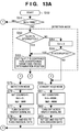
- Fig. 6 is a flow chart showing general control operation in this embodiment.
- step S100 standby adjustment mode processing is executed to execute the adjustment mode for a predetermined period of time.
- the light sources A and B alternately emit light beams, and the detection levels of the photoelectric converter 24 are made uniform.
- the CPU 11 repeats a light source driving cycle a predetermined number of times (60 times; a total of 15 msec, in this embodiment), in which the light sources A and B alternately emit light beams, the photoelectric converter 24 receives the light beams, and negative feedback control is performed to set the value A/D-converted by the A/D converter 14 to a specific value. Thereafter, the flow advances to step S200 to execute the standby hold mode of stopping emission control on the light sources A and B for a predetermined period of time.
- the CPU 11 repeats a light source driving cycle a predetermined number of times (8,000 times; a total of 2 sec, in this embodiment), in which the light intensity fixing signal Fb is output to hold the emission intensity level set when the flow shifted from the standby adjustment mode in step S100, and alternate emission is stopped in this state. Thereafter, the flow returns to the standby adjustment mode in step S100.
- the flow advances to the pre-detection adjustment mode in step S300. Note that this detection state may be checked every several cycles.
- step S300 the CPU 11 executes the pre-detection adjustment mode of causing the light sources A and B to alternately emit light beams and making the detection levels of the photoelectric converter 24 uniform.
- the driving signal MS is output to the convey motor 41 to drive the convey motor so as to start conveying an identification target into the apparatus.
- the CPU 11 performs the same operation as the standby adjustment mode in step S100 a predetermined number of times (e.g., 60 times; a total of 15 msec, in this embodiment). The flow then advances to the detection mode in step S400.
- the CPU 11 In the detection mode in step S400, the CPU 11 outputs the light intensity fixing signal Fb to hold the emission intensity level set when the flow advances from the pre-detection adjustment mode in step S300. While this state is held, the light sources A and B alternately emit light beams, and the sampling circuit 15 samples the output Vo from the amplifier circuit 27 in every cycle. In addition, the CPU 11 determines the current state by checking Pi 32, Ps 33, Pe 34, and Pr 35 in every cycle. After the CPU 11 repeats this operation a predetermined number of times (8,000 times or less in this embodiment), the flow returns to the standby adjustment mode in step S100.
- step S200 If no identification target is detected after a lapse of a predetermined period of time in the standby hold mode processing in step S200, the flow advances to the processing in step S100 after a lapse of a predetermined period of time.
- the CPU 11 then alternately executes the processing in step S100 and the processing in step S200.
- the CPU 11 stops light emission during the execution of the processing in step S200 instead of always alternately causing the light sources A and B to emit light beams, thereby suppressing a decrease in the service life of each light source.
- the control operation shown in Fig. 6 and driving control on the convey motor 41 are switched every time the count value of a counter Mct for counting light source driving cycles reaches a predetermined count value.
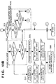
- Fig. 7 shows the count value of the counter Mct and each operation control switching timing.
- Fig. 7 is a timing chart showing the operation of this embodiment.
- the upper, intermediate, and lower portions of Fig. 7 respectively indicate the counter value of the counter Mct, the respective operation modes in Fig. 6, and the control timing of the convey motor 41 and light sources.
- the execution of the standby hold mode is started when the Mct count value becomes Swk1, and is kept executed until the count value becomes Swk2.
- the flow advances to the standby adjustment mode, and the Mct count value is set to Swt1. This mode is executed until the Mct count value becomes Swt2.
- the light intensity fixing signal Fb is set to be adjustable, and the light sources A and B alternately emit light beams to perform light intensity adjustment.
- the Mct count value becomes Swt2
- the Mct count value is preset to Swk1
- the flow advances to the standby hold mode. If the input sensor (Pi) 32 detects the insertion of an identification target in the above standby hold mode, the flow advances to the pre-detection adjustment mode while presetting the Mct count value to Sdt1 to drive the convey motor 41 so as to convey the identification target to the identification area.
- the light intensity fixing signal Fb is set to be adjustable, and the light sources A and B alternately emit light beams, thereby performing light intensity adjustment.
- the Mct count value becomes Sdt2
- the pre-detection adjustment mode is terminated, and the detection adjustment result is fixed.
- the Mct count value is then preset to Sdc1 to start the detection mode.
- the CPU 11 keeps driving the convey motor 41 to convey the identification target to the identification area, and waits for the arrival of the identification target at the position of the identification start sensor (Ps) 33. If the interruption of light is detected, a counter Ect for counting pulse signals Rck generated by the rotation sensor (Pr) 35 starts counting.
- the properties of the identification target are obtained to perform determination by checking the sampled value of the reception output Vo and the position of the identification target specified by the count value of the counter Ect in correspondence with each other.
- the detection mode is terminated, and the Mct count value is preset to Swt1. The flow then advances to the standby adjustment mode.
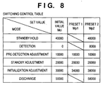
- Fig. 8 shows examples of the set values of the Mct count values in the respective modes.
- "initial value (Mci)” is a preset value at the start of the execution of mode processing
- preset 2 (Mp2) is an Mct count value at the time of the end of mode processing
- preset 1 (Mp1) indicates the alternate switching timing of the light sources A and B, which will be described later.
- preset 1 (Mp1) is the count value that shows the switching timing of the first adjustment and second adjustment described in the second embodiment. Note that the switching control table shown in Fig. 8 is stored in the memory 12.
- Fig. 9 is a flow chart showing operation in a light source driving cycle in this embodiment.
- Fig. 10 is a timing chart showing the relationship between the light source driving cycle and a signal generated by a timer and sent to the CPU in this embodiment.
- reference symbol Mct denotes a counter incremented in every light source driving cycle. The value of the counter Mct is set to fall within a specific range in each operation mode. Each mode can therefore be identified by only checking the value of the counter Mct.
- step S1 as shown in Fig. 5 DD1 is output to the output port (DD) to switch from the light source B driving state to the light source A driving state. UD2 is reset to "0".
- step S2 the first processing (to be described in detail later) is executed. In this case, if sampling and A/D conversion are started in the second half period of the previous cycle, evaluation of conversion data, determination, processing, and the like are performed.
- step S3 the Mct counter is incremented by one to count the number of times this light source driving cycle is executed.
- step S11 DD2 is output to DD to switch from the light source A driving state to the light source B driving state.
- UD1 is reset to "0" in advance.
- step S12 execute mode selection state check processing, thereby performing mode continuation or shift determination corresponding to each operation mode, initialization upon shift, a check on the position of the identification target, and the like.
- step S13 the second process is executed.
- a conversion start signal is output to the sampling circuit 15 and A/D converter 14 at a predetermined timing after a preparation for conversion is made.
- step S14 the CPU 11 confirms that UD2 is "0".
- step S15 the CPU 11 monitors whether UD2 changes to "1". If UD2 becomes "1", the flow returns to step S1 to perform emission control on the light source A.
- the timer 13 periodically outputs the first half period end signal UD1 associated with the light source driving cycle, the second half period end signal UD2 thereof, and an A/D conversion start signal ADT to the CPU 11 with predetermined time lags being kept among the respective signals.
- UD1, UD2 UD1 UD2
- ADT change from "0" to "1".
- the counter Gct is reset to continue a series of operations.
- UD1, UD2, and ADT are reset from “1" to "0" under the control of the CPU 11 after they are detected by the CPU 11.
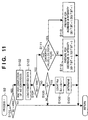
- Fig. 11 shows the first process in step S2 in Fig. 9 in detail.
- the Mct count value is equal to or less than "40,000", which indicates a mode other than the discharge or standby hold mold. If the count value is not equal to or less than "40,000", since the standby hold mode is set, and no A/D conversion data needs to be loaded, the flow returns.
- step S101 If it is determined in step S101 that the Mct count value is equal to or less than "40,000" , the detection mode and each adjustment mode are set, and a value has been sampled and A/D conversion has been started in step S13. The flow therefore advances to step S102. If the end of conversion is confirmed by checking the conversion end signal, the flow advances to step S103. In step S103, the data from the A/D converter 14 is loaded into the CPU 11.
- step S104 whether the Mct count value is equal to or more than "10,000" is checked to determine whether the light intensity adjustment mode or detection mode is set.
- step S105 it is checked whether a confirmation signal Fjp is stored.
- the confirmation signal Fjp is a marker indicating that the position of the identification target 100 can be specified.
- step S53 the confirmation signal Fjp is stored or set when a predetermined clock change of the pulse output Rck from the rotation sensor (Pr) 35 is confirmed between the previous light source driving cycle and the current cycle. If there is no confirmation signal Fjp, it is determined that the identification target 100 is not located at a position where its position should be determined, and the flow returns without performing determination.
- step S105 If it is determined in step S105 that the confirmation signal Fjp is present, the flow advances to step S106 to count Rck and increment Ect by one. In step S107, determination processing is executed at the corresponding point, and the flow returns.
- step S104 If it is determined in step S104 that the Mct count value is "10,000" or more, the flow advances to step S111 to compare the A/D-converted data value of the AC output signal Vo loaded in step S103 with a predetermined digital value corresponding to the reference voltage V1. If the reference voltage V1 is higher, the flow advances to step S112 to set the T bits of DD1 and DD2 to "0" to make a preparation for decreasing the light intensity of the light source B. The flow then returns.
- step S111 If it is determined in step S111 that the reference voltage V1 is lower, the flow advances to step S113 to set the T bits of DD1 and DD2 to "1" to make a preparation for increasing the light intensity of the light source B. The flow then returns.
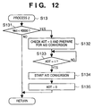
- Fig. 12 shows the detailed second process in step S13 in Fig. 9.
- step S131 first of all it is checked in step S131 whether the Mct count value is "40,000" or less which indicates a mode other than the discharge or standby hold mode shown in Fig. 8. If the Mct count value is not "40,000" or less, since it indicates that the standby hold mode is set, the flow returns without performing A/D conversion.
- step S131 If it is determined in step S131 that the Mct count value is "40,000" or less, since it indicates that a mode in which A/D conversion should be performed is set, the flow advances to step S132. It is then confirmed that the ADT signal is "0" before the A/D conversion timing in Fig. 10, and a preparation for A/D conversion processing is made.
- step S133 the CPU 11 monitors whether the A/D conversion timing has come, and the ADT signal becomes "1". If the A/D conversion timing has come, and the ADT signal becomes "1", the flow advances from step S133 to step S134 to output a conversion start signal to the sampling circuit 15 and A/D converter 14. The ADT signal is then set to "0", and the flow returns.
- step S51 first of all it is checked in step S51 whether the Mct count value is 10,000 or more, i.e., the detection mode is set. If the Mct count value is not 10,000 or more, since the detection mode is set, the flow advances to step S52 to check whether the Ps 33 or Pe 34 has detected the identification target 100, i.e., the identification target 100 is located in the identification area.
- step S52 If it is determined in step S52 that the Ps 33 or Pe 34 has detected the identification target 100, the flow advances to step S53 to check the Pr 35 and compare its current value with the value detected by the Pr 35 and stored in the previous cycle. If a predetermined change in value is determined, it is determined that the identification target 100 has been conveyed by a predetermined amount. In this case, it is determined that a cycle in which the position of the identification target 100 can be specified is set, and the confirmation signal Fjp is stored. In addition, the value detected by the Pr 35 and stored in the previous cycle is updated to the detection value in the current cycle.
- step S52 If it is determined in step S52 that neither the Ps 33 nor the Pe 34 have detected the identification target 100, it is determined that the identification target has not reached the position of the identification start sensor (Ps) 33. The flow then advances to step S54 to reset the counter Ect to "0", which counts Pr signals for specifying the position of the identification target from the identification start position.
- step S55 it is checked whether the input sensor Pi 32 has detected the identification target. If the input sensor Pi 32 has detected the identification target, it is determined that the leading edge of the identification target is located between the Pi 32 and the Ps 33. Thereafter, the identification target is conveyed upon rotation of the convey motor 41 and reaches the position of the Ps 33. The flow therefore advances to step S53.
- step S55 If it is determined in step S55 that the input sensor Pi 32 has not detected the identification target, since a detection error may be present in the input sensor, the flow advances to the standby hold mode in step S60 and the subsequent steps.
- step S60 the count value of the Mct count value is set to 40,000, and preset 2 (Mp2) is set to 48,000.
- step S62 the MS signal is turned off to perform control so as not to drive the convey motor 41.
- step S63 DD1 and DD2 as driving pulse data outputs are set to non-emission data. The flow then returns.
- step S51 If it is determined in step S51 that the Mct count value is 10,000 or more, since the detection mode is not set, the flow advances to step S71 to check whether the Mct count value is 40,000 or more, i.e., an operation mode in which the light sources are not turned on, e.g., the standby hold mode, is set. If the Mct count value is not 40,000 or more, since the standby adjustment more or pre-detection adjustment mode is set, the flow advances to step S72 to check whether the Mct count value is equal to preset 2 (Mp2). If the Mct count value is not equal to preset 2 (Mp2), since it indicates that the adjustment mode has not been completed, the flow returns.
- Mp2 preset 2
- step S73 If the Mct count value becomes equal to preset 2 (Mp2), the flow advances to step S73. If the Mct count value is 20,000 or less, and the pre-detection adjustment mode is set, the detection mode in step S75 and the subsequent steps is started.
- step S76 the count value of the counter Mct is reset to "0", and preset 2 (Mp2) is set to 8,000 to execute the detection mode afterward.
- the MS signal is enabled to continuously drive the convey motor 41, which has already been driven, in step S77.
- DD1 and DD2 as driving pulse data outputs are then set to fixed emission data. The flow then returns. With this operation, the emission intensities are fixed, and the identification target passes through the identification area.
- step S73 If it is determined in step S73 that the Mct count value is not 20,000 or less, since it indicates that the standby adjustment or initialization adjustment is performed, the flow advances to the standby hold mode in step S60 and the subsequent steps.
- the Mct count value is set to 40,000, and preset 2 (Mp2) is set to 48,000 to shift to the hold mode.
- step S62 the MS signal is turned off (disabled) to stop the convey motor 41.
- DD1 and DD2 as driving pulse data outputs are set to non-emission data. The flow then returns.
- step S71 If it is determined in step S71 that the Mct count value is 40,000 or more, it indicates that the standby hold mode or discharge mode is being executed.
- the flow then advances to S81 to check whether light received by the input sensor (Pi) is interrupted, and an identification target is inserted into the apparatus. If light received by the input sensor (Pi) is not interrupted, the flow advances to step S82 to check whether the Mct count value becomes equal to preset 2 (Mp2), and the operation under execution is complete. If the Mct count value is not equal to preset 2 (Mp2), the flow returns.
- step S82 If it is determined in step S82 that the Mct count value is equal to preset 2 (Mp2), the flow advances to the standby adjustment mode in step S85 and the subsequent steps.
- step S86 the Mct count value is set to 20,000, and preset 2 (Mp2) is set to 20,060.
- step S87 the MS signal is turned off (disabled) to stop the convey motor 41.
- step S88 DD1 and DD2 as driving pulse data outputs are set to adjustment emission data. The flow then returns.
- step S81 If it is determined in step S81 that light received by the input sensor (Pi) is interrupted, and an identification target is inserted into the apparatus, the Mct count value is set to 10,000 and preset 2 (Mp2) is set to 10,060 to shift to the pre-detection adjustment mode in step S91 and the subsequent steps.
- step S93 the MS signal is turned on to drive the convey motor 41 to insert the identification target into the apparatus, and pre-detection adjustment is executed at the same time.
- step S88 DD1 and DD2 as driving pulse data outputs are set to adjustment emission data. The flow then returns.
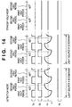
- Fig. 14 shows examples of driving control signals and detection signal timings for the light source A/light source B 23 in the detection mode and standby hold mode in the above control.
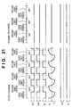
- Fig. 15 shows examples of driving control signals and detection signal timings for the light source A/light source B 23 in the standby adjustment mode and pre-detection adjustment mode. Note that the detection output Vo is indicated in opposite phase to become lower than the reference voltage V1 when one light source that is dominant with respect to the other light source emits light.
- control operation is performed to set a detection output sampled value to the reference voltage V1 before an identification target reaches the detection range.
- the output of the log amplifier 25 at the sampling timing is also controlled to a predetermined voltage.
- the photoelectric converter 24 When the identification target reaches the detection range while the amounts of light beams emitted from the light source A/light source B 23 in this control state are fixed, the photoelectric converter 24 outputs an electrical signal corresponding to the wavelength of light emitted from each light source 23 and having passed through the identification target. This signal is amplified by the log amplifier 25 and output to the high-pass filter 26.
- the waveform of the output Vo in Fig. 14 and 15 is opposite in phase to a change in light amount. For this reason, if, for example, the color of the identification target in the detection range is reddish rather than greenish (the transmittance degree of light from the light source A is higher) when the light source A is a red and the light source B is a green the output voltage of a signal at the light source A emission timing becomes smaller than that of a signal at the light source B emission timing in the case shown in Fig. 14.
- the output voltage value of a signal at the light source B emission timing becomes smaller than that of a signal at the light source A emission timing.
- the color of the identification target in the detection range is reddish rather than greenish, and hence the output voltage value of a signal at the light source A emission timing is smaller than that of a signal at the light source B emission timing.
- the color of the identification target in the detection range is greenish rather than reddish, and hence the output voltage value of a signal at the light source B emission timing is smaller than that of a signal at the light source A emission timing.
- the high-pass filter 26 removes components having frequencies less than the light source driving frequency from a detection signal to extract only AC components having frequencies equal to or higher than the light source driving frequency.
- the amplifier circuit 27 amplifies the lighit source driving frequency and superimposes the reference voltage V1 on the extracted components.
- the sampling circuit 15 samples waveform data at the detection timing (second half period of a light source driving cycle) of light emitted from the light source B from this superimposed waveform.
- the A/D converter 14 A/D-converts the sampled data. The resultant data is stored in the form of a digital value until the next A/D conversion.
- the amplifier circuit 27 outputs a signal that oscillates to the positive or negative side with respect to the reference voltage V1 in proportion to changes (the difference between detection signals when the photoelectric converter 24 receives light beams from the two light sources) in the amounts of light beams detected from the light sources A and B.
- the extent to which the color of an identification target is reddish (when the signal oscillates to the positive side) or the extent to which the color of an identification target is greenish (when the signal oscillates to the negative side) can be detected by only sampling a signal at the detection timing of light emitted from the light source B.
- the CPU 11 loads the signal level of a detection signal change (color appearance and degree) caused upon switching from the light source A to the light source B, which is the sampling result obtained by the sampling circuit 15. As shown in Fig. 14, in this embodiment the tendency of the color of an identification target with respect to light beams emitted from the light source A/light source B 23 is output as one signal.
- the CPU 11 therefore compares this detection signal pattern with the standard pattern obtained by detecting an authentic identification target (negotiable instrument or the like) and registered in the memory 12 in advance at predetermined convey intervals, thereby determining the degree of similarity. If a predetermined degree of similarity or higher is determined, the identification target is identified as an authentic one.
- Figs. 16 and 17 show sampling results with respect to a predetermined identification target (using a proper color chart) in this embodiment.
- Fig. 16 shows the sampling result obtained with respect to the identification target when green and red light-emitting diodes are respectively used as the light sources A and B.
- Fig. 17 shows the sampling result obtained with respect to the identification target when an infrared light-emitting diode and red light-emitting diode are respectively used as the light sources A and B.
- the identification target is reddish, bluish, or greenish, i.e., a color arrangement, cannot be accurately determined, high-sensitivity detection can be performed within the green gamut.
- a light-transmitting object identifying apparatus which can automatically solve problems associated with variations in performance of each constituent member of a mechanism for detecting an identification object, changes in performance over time, and changes in performance due to environments with a simple arrangement, can be easily manufactured and adjusted, and has high reliability.
- a deterioration in the light sources can be minimized because the apparatus is designed to perform detection sensitivity adjustment at predetermined intervals and inhibit the light sources from emitting light while no adjustment is performed, in the absence of an identification target, instead of performing adjustment by always causing the light sources to emit light.
- the light source 23 has two light sources, and the photoelectric converter 24 is used to detect light beams emitted from the two light sources and transmitted through an identification target.
- the present invention is not limited to the above arrangement.
- the light source may be constituted by a plurality of light sources.
- the light source A may be constituted by light sources A1 and A2.
- the emission intensities of the light sources can be made uniform by using a method of adjusting the emission intensities of the light sources A1 and A2 by causing them to emit light beams at a timing B while the emission of the light source B is stopped, and then adjusting the light source A (constituted by the light sources A1 and A2) and the light source B after returning the emission timing of the light source A2 to a timing A. Since the adjustment can be realized by the same operation as that described above except for switching of the light source driving circuit, the circuit arrangement can be simplified.
- a composite light source constituted by green and infrared LEDs and a red LED makes it easy to detect bluish and greenish colors as compared with the case wherein green and red LEDs are used.
- the second embodiment of the present invention in which a light source is constituted by a plurality of light sources, will be described below.
- the same reference numerals as in the first embodiment denote the same parts in the second embodiment described below, and a detailed description thereof will be omitted.
- Fig. 18 shows the arrangement of a negotiable instrument identifying apparatus according to the second embodiment of the present invention.
- the second embodiment shown in Fig. 18 includes a light source A1 driving circuit 121 having an arrangement similar to that of the light source A driving circuit 21 in the first embodiment shown in Fig. 1, and differs from the first embodiment in that the second embodiment also includes a light source A2 intensity changing/driving circuit 122 and a composite light source 123 constituted by light sources A1, A2, and B.
- a light source A1 blink signal Sa1 similar to the light source A blink signal Sa, light source A2 blink signal Sa2, and light intensity fixing signal Fa2 are prepared.
- the light source A shown in Fig. 18 is made of light sources A1 and A2
- the light source A2 is caused to emit light at the timing of the light source B to adjust the emission intensities of the light sources A1 and A2 while the emission of the light source B is stopped in the first adjustment emission.
- the emission intensities of the composite light source can be made uniform by using the method of adjusting the emission intensities of the light sources A1 and A2 first, restoring the timing of the light source A2 to that of the light source A after the second adjustment emission process, and then adjusting the light source A (constituted by the light sources A1 and A2).
- the circuit arrangement can be simplified.
- Figs. 19A to 19D show control data for the output port of the CPU 11, which outputs six types of light source control signal (each consisting of one bit) in the second embodiment.
- the values of DD1 and DD2 are set in a control procedure to which the operation mode shifts. By alternately outputting combinations of two values of DD1 and DD2 to the output port, alternate control on the light sources which is unique to each mode is performed.
- Fig. 19A shows control data set in a fixed emission mode (detection mode);
- Fig. 19B control data in the first adjustment emission mode (standby adjustment mode or pre-detection adjustment mode) of adjusting emission intensity;
- Fig. 19C control data in the second adjustment emission mode (standby adjustment mode or pre-detection adjustment mode) of adjusting emission intensity;
- Fig. 19D control data set in a non-emission mode (standby hold mode).
- the light intensity fixing signals Fa2 and Fb become "1" regardless whether DD1 or DD2 is output, and the analog switch circuit described above is open at this time. Therefore, the light intensities set when the analog switch circuit was opened are fixed.
- the light source A constituted by the light sources A1 and A2
- the light source B are caused to alternately emit light while certain light intensities are fixed.
- the value of the light intensity adjustment signal T may be either "1" or "0" because it does not influence the emission condition.
- the light intensity fixing signal Fb is "1" regardless of whether DD1 or DD2 is output, and hence the light source B keeps its light intensity level while stopping light emission.
- the light intensity fixing signal Fa2 is "0" regardless of whether DD1 or DD2 is output, and the above analog switch circuit is on at this time. For this reason, while “0" is output as the light intensity adjustment signal T, the light intensity of the light source A2 decreases. In contrast to this, while "1" is output, the light intensity of the light source A2 increases.
- the light source B holds its light intensity level while stopping light emission, and intensity adjustment of the light source A2 is performed to always bring sampled values near to a reference value while the light sources A1 and A2 are caused to alternately emit light.
- the light source A1 blink signal Sa1, light source A2 blink signal Sa2, and light source B blink signal Sb respectively become “0", “0", and "1". As a consequence, only the light source B emits light.
- the light intensity fixing signal Fa2 is "1" regardless of whether DD1 or DD2 is output, and hence the light intensity of the light source A2 is fixed.
- the light intensity fixing signal Fb is "0" regardless of whether DD1 or DD2 is output, and the above analog switch circuit is on at this time. For this reason, while “0" is output as the light intensity adjustment signal T, the light intensity of the light source B decreases. In contrast to this, while "1" is output, the light intensity of the light source B increases.
- intensity adjustment of the light source B is performed to always bring sampled values near to a reference value while the light sources A and B constituting the composite light source whose light intensity ratio is fixed are caused to alternately emit light.
- each of the light source A1 blink signal Sa1, light source A2 blink signal Sa2, and light source B blink signal Sb becomes "0" regardless of whether DD1 or DD2 is output.
- Each of the light intensity fixing signals Fa2 and Fb becomes "1" regardless of whether DD1 or DD2 is output, and the above analog switch circuit is open. The voltage values for defining light intensities which were set when the analog switch circuit was opened are fixed.
- the light intensity adjustment signal T may be "1" or "0" because its value does not influence the emission condition.
- the light sources can be controlled by alternately outputting DD1 and DD2.
- the general control in the second embodiment having the above arrangement is the same as that in the first embodiment except for mode selection state check processing.
- the mode selection state check processing in the second embodiment will be described with reference to Figs. 20A and 20B.
- step S201 first of all it is checked in step S201 whether a Mct count value is equal to or larger than 50,000, i.e., the discharge mode is set. If the Mct count value is not 50,000 or more, the flow advances to step S202 to check whether the Mct count value is 10,000 or more.
- step S203 the flow advances to step S203 to check whether the Mct count value is equal to the value of preset 2 (Mp2). If the Mct count value is not equal to the value of preset 2 (Mp2), the flow advances to step S204 to check whether a Ps 33 or Pe 34 has detected an identification target 100, i.e., the identification target 100 is in the identification area.
- step S210 the flow advances to step S210 to check a Pr 35 and compare the current value with the detection value stored in the Pr 35 in the previous cycle. If there is a predetermined change, it is determined that the identification target 100 has been conveyed by a predetermined amount.
- the current cycle is determined as a cycle in which the position of the identification target 100 can be specified, and a confirmation signal Fjp is stored.
- the detection value stored in the Pr 35 in the previous cycle is updated to the detection value in the current cycle, and the flow returns.
- step S204 If it is determined in step S204 that neither the Ps 33 nor the Pe 34 have detected the identification target 100, it is determined that the identification target has not reached the position of the identification start sensor (Ps) 33.
- the flow then advances to step S205 to reset a counter Ect for a Pr signal for specifying the position of the identification target from the identification start position to 0.
- step S206 it is checked whether the input sensor Pi 32 has detected the identification target.
- step S206 If it is determined in step S206 that the input sensor Pi 32 has not detected the identification target, since a detection error may be caused in the input sensor, the flow advances to the standby hold mode in step S207 and the subsequent steps.
- step S207 the count value of the counter Mct is set to 40,000, and preset 1 (Mp1) and preset 2 (Mp2) are respectively set to 60,000 and 48,000.
- step S208 an MS signal is turned off to inhibit a convey motor 41 from being driven.
- step S209 DD1 and DD2 as driving pulse data outputs are set to non-emission data, and the flow returns.
- step S206 If it is determined in step S206 that the input sensor Pi 32 has detected the identification target, it is determined that the leading edge of the identification target is located between the Pi 32 and Ps 33. Since the identification target is conveyed upon rotation of the convey motor 41 and reaches the position of the Ps 33, the flow advances to step S210.
- step S210 the Pr 35 is checked, and the current values is compared with the detection value stored in the Pr 35 in the previous cycle. If there is a predetermined change, it is determined that the identification target 100 has been conveyed by a predetermined amount. In this case, the current cycle is determined as a cycle in which the position of the identification target can be specified, and the confirmation signal Fjp is stored.
- the detection value stored in the Pr 35 in the previous cycle is updated to the detection value in the current cycle, and the flow returns.
- step S212 the flow advances to step S212 to check whether the Ps 33 or Pe 34 has detected the identification target 100, i.e., the identification target 100 is in the identification area. If the Ps 33 or Pe 34 has detected the identification target 100 in such situation other than the detection mode, the flow advances to the discharge mode processing in step S213 and the subsequent steps.
- the discharge mode processing first of all in step S213 the count value of the counter Mct, preset 1 (Mp1), and preset 2 (Mp2) are respectively set to 50,000, 60,000, and 58,000.
- step S214 the MS signal is turned on to drive the convey motor 41 to convey the identification target and discharge it from the discharge position.
- step S209 DD1 and DD2 as driving pulse data outputs are set to non-emission data. The flow then returns.
- step S212 If it is determined in step S212 that neither the Ps 33 nor the Pe 34 have detected the identification target 100, the flow advances to step S215 to check whether the Mct count value is 40,000 or more, i.e., the standby hold mode of inhibiting the light sources from emitting light is set. If the Mct count value is not 40,000 or more, since the standby adjustment mode or detection mode is set, the flow advances to step S216 to check whether the Mct count value is equal to the value of preset 1 (Mp1). If the Mct count value is equal to the value of preset 1 (Mp1), the flow advances to the second adjustment mode in the step S222 to set adjustment emission data as the driving pulse data DD1 and DD2. The flow then returns.
- Mp1 the value of preset 1
- step S216 If it is determined in step S216 that the Mct count value is not equal to the value of preset 1 (Mp1), the flow advances to step S217 to check whether the Mct count value is equal to the value of preset 2 (Mp2). If the Mct count value is not equal to the value of preset 2 (Mp2), it is determined that the first or second adjustment mode is not complete. The flow then returns.
- step S217 When the Mct count value becomes equal to the value of the preset 2 (Mp2), the flow advances from step S217 to step S218 to check whether the Mct count value is 20,000 or less. If the Mct count value is not 20,000 or less, it is determined that the standby adjustment mode is complete, and the flow advances to the standby hold mode in step S 207 and the subsequent steps.
- Mp2 the value of the preset 2
- step S218 If it is determined in step S218 that the Mct count value is 20,000 or less, it is determined that the pre-detection adjustment mode is complete, and the flow advances to the detection mode in step S219 and the subsequent steps.
- step S219 the count value of the counter Mct, preset 1 (Mp1), and preset 2 (Mp2) are respectively set to 0, 60,000, and 8,000.
- step S220 the MS signal is turned on to continuously drive the convey motor 41.
- step S221 and DD2 as driving pulse data outputs are set to fixed emission data. The flow then returns.
- step S215 If it is determined in step S215 that the Mct count value is 40,000 or more, it indicates that the standby hold mode is being executed, and the flow advances to step S225 to check whether light to the input sensor (Pi) is interrupted and the identification target is inserted into the apparatus. If light to the input sensor (Pi) is not interrupted, the flow advances to step S226 to check whether the Mct count value is equal to preset 2 (Mp2) and the operation mode under execution is complete. If the Mct count value is not equal to preset 2 (Mp2), the flow returns.
- Mp2 preset 2
- step S226 If it is determined in step S226 that the Mct count value is equal to preset 2 (Mp2), the standby adjustment mode processing in step S227 and the subsequent steps is executed.
- step S227 the Mct count value, preset 1 (Mp1), and preset 2 (Mp2) are respectively set to 20,000, 20,030, and 20,060.
- step S2208 the MS signal is turned off (disabled) to stop the convey motor 41.
- step S229 DD1 and DD2 as driving pulse data outputs are set to adjustment emission data. The flow then returns.
- step S225 If it is determined in step S225 that light to the input sensor (Pi) is interrupted and the identification target is inserted into the apparatus, the flow advances to the pre-detection adjustment mode in the step S230 and the subsequent steps, and the Mct count value, preset 1 (Mp1), and preset 2 (Mp2) are respectively set to 10,000, 10,030, and 10,060.
- step S231 the MS signal is turned on to drive the convey motor 41.
- step S229 DD1 and DD2 as driving pulse data outputs are set to first adjustment emission data. The flow then returns.
- step S201 If it is determined in step S201 that the Mct count value is 50,000 or more (the discharge mode in the second embodiment), the flow advances to step S240 to check whether the Pi 32, Ps 33, or Pe 34 has detected the identification target 100, i.e., the identification target 100 is located in the apparatus. If the Pi 32, Ps 33, or Pe 34 has detected the identification target 100, the flow returns.
- step S240 If it is determined in step S240 that none of the Pi 32, Ps 33, and Pe 34 have detected the identification target 100, the flow advances to step S241 to check whether the Mct count value is equal to preset 2 (Mp2) and the discharge mode under execution is complete. If the Mct count value is not equal to preset 2 (Mp2), the flow returns.
- step S241 If it is determined in step S241 that the Mct count value is equal to preset 2 (Mp2), the initialization adjustment mode processing in step S242 and the subsequent steps is executed.
- step S242 the Mct count value, preset 1 (Mp1), and preset 2 (Mp2) are respectively set to 30,000, 34,000, and 38,000.
- step S243 the MS signal is turned off (disabled) to stop the convey motor 41.
- step S229 DD1 and DD2 as driving pulse data outputs are set to adjustment emission data. The flow then returns.
- Fig. 21 shows examples of driving control signals for the light sources A1, A2, and B123 and detection signal timings in the detection mode and standby hold mode under the control described above.
- Fig. 22 shows examples of driving control signals for the light sources A1, A2, and B123 and detection signal timings in the standby adjustment mode and pre-detection adjustment mode.
- Fig. 23 shows the sampling result obtained by performing sampling operation in this manner with respect to a predetermined identification target in the second embodiment. In the case shown in Fig. 23, a green LED, infrared LED, and red LED are respectively used as the light source A1, light source A2, and light source B.
- each of the standby adjustment mode and pre-detection adjustment mode is divided into two parts.
- the light sources A1 and A2 are adjusted.
- the light sources A1 and A2 and light source B are adjusted (e.g., 30 times + 30 times; a total of 15 msec).
- red and green light-emitting diodes or a red light-emitting diode, infrared light-emitting diode, and green light-emitting diode are installed in one place, and light beams are received by one photoelectric converter.
- the present invention is not limited to this, and may be constituted by a plurality of combinations of detection systems (a light source, light source driving circuit, photoelectric converter, and light-receiving amplifier unit).
- the third embodiment may have the same basic arrangement as that of the first embodiment.
- blinking of each light source and fixing of light intensity may be concurrently controlled at the same timing, and signal data processing such as sampling and light intensity adjustment may be performed in light source driving cycles in a time-divisional manner.
- the third embodiment is constituted by the two detection systems in the first embodiment.
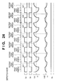
- Fig. 24 shows examples of driving control signals for the light sources and detection signal timings in the detection mode according to the third embodiment.
- Fig. 25 shows examples of driving control signals for the light sources and detection signal timings in the standby adjustment mode and pre-detection adjustment mode.
- the duty ratio of driving pulses for the light sources is nearly 50%.
- the present invention is not limited to a duty ratio of 50%, and an arbitrary duty ratio can be set.
- a light-transmitting object identifying apparatus which can automatically solve problems associated with variations in performance of each constituent member of a mechanism for detecting an identification object, changes in performance over time, and changes in performance due to environments with a simple arrangement, can be easily manufactured and adjusted, and has high reliability.
- reliable authentication can be performed using a simple algorithm.
- the light sources do not emit light unnecessarily, the reliability of each light source can be greatly improved.
Landscapes
- Health & Medical Sciences (AREA)
- General Health & Medical Sciences (AREA)
- Toxicology (AREA)
- Physics & Mathematics (AREA)
- General Physics & Mathematics (AREA)
- Geophysics And Detection Of Objects (AREA)
- Inspection Of Paper Currency And Valuable Securities (AREA)
- Photometry And Measurement Of Optical Pulse Characteristics (AREA)
- Investigating Or Analysing Materials By Optical Means (AREA)
Priority Applications (1)
| Application Number | Priority Date | Filing Date | Title |
|---|---|---|---|
| EP07010495A EP1840848A3 (fr) | 1999-05-28 | 2000-05-23 | Appareil et procédé d'identification d'objet électroluminescent |
Applications Claiming Priority (2)
| Application Number | Priority Date | Filing Date | Title |
|---|---|---|---|
| JP15011099A JP3866878B2 (ja) | 1999-05-28 | 1999-05-28 | 光透過物の識別装置及び方法 |
| JP15011099 | 1999-05-28 |
Related Child Applications (1)
| Application Number | Title | Priority Date | Filing Date |
|---|---|---|---|
| EP07010495A Division EP1840848A3 (fr) | 1999-05-28 | 2000-05-23 | Appareil et procédé d'identification d'objet électroluminescent |
Publications (1)
| Publication Number | Publication Date |
|---|---|
| EP1056057A1 true EP1056057A1 (fr) | 2000-11-29 |
Family
ID=15489717
Family Applications (2)
| Application Number | Title | Priority Date | Filing Date |
|---|---|---|---|
| EP00110290A Withdrawn EP1056057A1 (fr) | 1999-05-28 | 2000-05-23 | Dispositif et procédé pour l'identification d'objets transmettant la lumière |
| EP07010495A Withdrawn EP1840848A3 (fr) | 1999-05-28 | 2000-05-23 | Appareil et procédé d'identification d'objet électroluminescent |
Family Applications After (1)
| Application Number | Title | Priority Date | Filing Date |
|---|---|---|---|
| EP07010495A Withdrawn EP1840848A3 (fr) | 1999-05-28 | 2000-05-23 | Appareil et procédé d'identification d'objet électroluminescent |
Country Status (5)
| Country | Link |
|---|---|
| US (2) | US6483095B1 (fr) |
| EP (2) | EP1056057A1 (fr) |
| JP (1) | JP3866878B2 (fr) |
| KR (1) | KR100335603B1 (fr) |
| CA (1) | CA2308644C (fr) |
Cited By (2)
| Publication number | Priority date | Publication date | Assignee | Title |
|---|---|---|---|---|
| EP2230647A1 (fr) * | 2006-09-29 | 2010-09-22 | Aruze Corp. | Dispositif d'identification de feuille |
| DE10341327B4 (de) * | 2002-09-11 | 2017-07-20 | Omron Corp. | Photoelektrischer Sensor |
Families Citing this family (12)
| Publication number | Priority date | Publication date | Assignee | Title |
|---|---|---|---|---|
| JP3866878B2 (ja) * | 1999-05-28 | 2007-01-10 | 株式会社日本コンラックス | 光透過物の識別装置及び方法 |
| JP3706807B2 (ja) * | 2001-01-24 | 2005-10-19 | キヤノン株式会社 | 画像入力システム |
| JP2002245511A (ja) | 2001-02-15 | 2002-08-30 | Hitachi Ltd | 紙質識別方法 |
| JP2003032435A (ja) * | 2001-07-18 | 2003-01-31 | Canon Inc | 画像認識装置 |
| JP3839342B2 (ja) * | 2002-04-11 | 2006-11-01 | 株式会社リコー | 給紙装置及びそれを備えた画像形成装置 |
| US8718919B2 (en) * | 2002-04-23 | 2014-05-06 | Robert Bosch Gmbh | Method and apparatus for lane recognition for a vehicle |
| WO2007109760A2 (fr) * | 2006-03-22 | 2007-09-27 | The Curators Of The University Of Missouri | Appareil et procede d'evaluation de la neutralisation visuelle |
| US8682056B2 (en) * | 2008-06-30 | 2014-03-25 | Ncr Corporation | Media identification |
| US8255820B2 (en) | 2009-06-09 | 2012-08-28 | Skiff, Llc | Electronic paper display device event tracking |
| DE102009054067A1 (de) * | 2009-11-20 | 2011-05-26 | Osram Opto Semiconductors Gmbh | Licht emittierende Vorrichtung |
| US9875594B2 (en) * | 2013-02-20 | 2018-01-23 | Crane Payment Innovations, Inc. | Banknote validator |
| JP7656160B2 (ja) * | 2020-02-07 | 2025-04-03 | 富士通オプティカルコンポーネンツ株式会社 | 制御装置および制御方法 |
Citations (6)
| Publication number | Priority date | Publication date | Assignee | Title |
|---|---|---|---|---|
| JPS5466894A (en) | 1977-11-07 | 1979-05-29 | Omron Tateisi Electronics Co | Banknote color detecting apparauts |
| US4587434A (en) * | 1981-10-22 | 1986-05-06 | Cubic Western Data | Currency note validator |
| US4618257A (en) * | 1984-01-06 | 1986-10-21 | Standard Change-Makers, Inc. | Color-sensitive currency verifier |
| JPS62111377A (ja) * | 1985-11-11 | 1987-05-22 | 富士電機株式会社 | 紙幣等の光学的識別方式 |
| US4769532A (en) * | 1986-07-11 | 1988-09-06 | Laurel Bank Machines Co., Ltd. | Apparatus for adjusting optical sensors with threshold memory |
| JPH1186073A (ja) * | 1997-09-10 | 1999-03-30 | Yokohama Denshi Kogyo Kk | 有価証券識別装置及び方法 |
Family Cites Families (2)
| Publication number | Priority date | Publication date | Assignee | Title |
|---|---|---|---|---|
| JP3866878B2 (ja) * | 1999-05-28 | 2007-01-10 | 株式会社日本コンラックス | 光透過物の識別装置及び方法 |
| JP3933826B2 (ja) * | 1999-12-14 | 2007-06-20 | 株式会社日本コンラックス | 紙葉類の光学的識別装置 |
-
1999
- 1999-05-28 JP JP15011099A patent/JP3866878B2/ja not_active Expired - Fee Related
-
2000
- 2000-05-17 CA CA002308644A patent/CA2308644C/fr not_active Expired - Fee Related
- 2000-05-18 US US09/573,383 patent/US6483095B1/en not_active Expired - Fee Related
- 2000-05-23 EP EP00110290A patent/EP1056057A1/fr not_active Withdrawn
- 2000-05-23 EP EP07010495A patent/EP1840848A3/fr not_active Withdrawn
- 2000-05-27 KR KR1020000028887A patent/KR100335603B1/ko not_active Expired - Fee Related
-
2002
- 2002-07-11 US US10/194,841 patent/US6642502B2/en not_active Expired - Fee Related
Patent Citations (6)
| Publication number | Priority date | Publication date | Assignee | Title |
|---|---|---|---|---|
| JPS5466894A (en) | 1977-11-07 | 1979-05-29 | Omron Tateisi Electronics Co | Banknote color detecting apparauts |
| US4587434A (en) * | 1981-10-22 | 1986-05-06 | Cubic Western Data | Currency note validator |
| US4618257A (en) * | 1984-01-06 | 1986-10-21 | Standard Change-Makers, Inc. | Color-sensitive currency verifier |
| JPS62111377A (ja) * | 1985-11-11 | 1987-05-22 | 富士電機株式会社 | 紙幣等の光学的識別方式 |
| US4769532A (en) * | 1986-07-11 | 1988-09-06 | Laurel Bank Machines Co., Ltd. | Apparatus for adjusting optical sensors with threshold memory |
| JPH1186073A (ja) * | 1997-09-10 | 1999-03-30 | Yokohama Denshi Kogyo Kk | 有価証券識別装置及び方法 |
Cited By (5)
| Publication number | Priority date | Publication date | Assignee | Title |
|---|---|---|---|---|
| DE10341327B4 (de) * | 2002-09-11 | 2017-07-20 | Omron Corp. | Photoelektrischer Sensor |
| EP2230647A1 (fr) * | 2006-09-29 | 2010-09-22 | Aruze Corp. | Dispositif d'identification de feuille |
| US8194236B2 (en) | 2006-09-29 | 2012-06-05 | Universal Entertainment Corporation | Sheet identifying device |
| US8300217B1 (en) | 2006-09-29 | 2012-10-30 | Universal Entertainment Corporation | Sheet identifying device |
| US8300216B2 (en) | 2006-09-29 | 2012-10-30 | Universal Entertainment Corporation | Sheet identifying device |
Also Published As
| Publication number | Publication date |
|---|---|
| EP1840848A2 (fr) | 2007-10-03 |
| JP3866878B2 (ja) | 2007-01-10 |
| US6642502B2 (en) | 2003-11-04 |
| US20020175301A1 (en) | 2002-11-28 |
| KR20010029755A (ko) | 2001-04-16 |
| EP1840848A3 (fr) | 2008-04-02 |
| CA2308644C (fr) | 2005-06-07 |
| JP2000339513A (ja) | 2000-12-08 |
| KR100335603B1 (ko) | 2002-05-08 |
| US6483095B1 (en) | 2002-11-19 |
| CA2308644A1 (fr) | 2000-11-28 |
Similar Documents
| Publication | Publication Date | Title |
|---|---|---|
| EP1056057A1 (fr) | Dispositif et procédé pour l'identification d'objets transmettant la lumière | |
| KR100274406B1 (ko) | 유가증권 식별장치 및 방법 | |
| EP1254435B1 (fr) | Appareil et procede d'authentification de documents | |
| GB2227093A (en) | Apparatus for adjusting optical sensors | |
| WO2004036508A2 (fr) | Procede et systeme d'authentication de devise a multilongueur d'onde | |
| EP1049054A3 (fr) | Dispositif discriminateur de pièces de monnaie | |
| KR101037430B1 (ko) | 검사장치 | |
| EP1056055A3 (fr) | Appareil discriminateur de pièces de monnaie | |
| JP2003077025A (ja) | 紙葉類判別装置及び紙葉類判別方法 | |
| JPS59604A (ja) | 対向照明形縁部検出装置 | |
| JP3960282B2 (ja) | 紙幣識別装置 | |
| WO2004097752A1 (fr) | Dispositif et procede d'identification de feuille | |
| US6400460B1 (en) | Multifunction optical sensor with variable detection threshold and noise suppression | |
| JP3309484B2 (ja) | 結晶方位検出方法および装置 | |
| JPH0944633A (ja) | 紙葉類鑑別装置 | |
| JP3971889B2 (ja) | 紙幣識別装置およびその制御方法 | |
| KR101974601B1 (ko) | 지폐 계수기의 더블 검지 센서구조 | |
| JP2001283281A (ja) | 紙葉類の蛍光スレッド検出装置 | |
| KR20030095770A (ko) | 지폐계수기용 크기센서의 신호처리장치 | |
| JP2007299154A (ja) | 紙幣識別装置 | |
| JP2002279479A (ja) | 紙幣検知装置 | |
| KR20000018517A (ko) | 지폐 인식 장치의 지폐 인식 감도 조절 방법 | |
| KR19990073025A (ko) | 위폐감식회로 | |
| JP2005190256A (ja) | 紙幣識別装置 | |
| KR19990073026A (ko) | 위폐감식장치 |
Legal Events
| Date | Code | Title | Description |
|---|---|---|---|
| PUAI | Public reference made under article 153(3) epc to a published international application that has entered the european phase |
Free format text: ORIGINAL CODE: 0009012 |
|
| AK | Designated contracting states |
Kind code of ref document: A1 Designated state(s): DE FR GB IT NL |
|
| AX | Request for extension of the european patent |
Free format text: AL;LT;LV;MK;RO;SI |
|
| 17P | Request for examination filed |
Effective date: 20010319 |
|
| AKX | Designation fees paid |
Free format text: DE FR GB IT NL |
|
| RAP1 | Party data changed (applicant data changed or rights of an application transferred) |
Owner name: KABUSHIKI KAISHA NIPPON CONLUX |
|
| 17Q | First examination report despatched |
Effective date: 20061212 |
|
| RIN1 | Information on inventor provided before grant (corrected) |
Inventor name: IWAKI, KUNIHIDE |
|
| RAP1 | Party data changed (applicant data changed or rights of an application transferred) |
Owner name: KABUSHIKI KAISHA NIPPON CONLUX |
|
| STAA | Information on the status of an ep patent application or granted ep patent |
Free format text: STATUS: THE APPLICATION IS DEEMED TO BE WITHDRAWN |
|
| 18D | Application deemed to be withdrawn |
Effective date: 20101111 |