EP1056128A2 - Dispositif semi-conducteur à mémoire et son procédé de manufacture - Google Patents
Dispositif semi-conducteur à mémoire et son procédé de manufacture Download PDFInfo
- Publication number
- EP1056128A2 EP1056128A2 EP00111276A EP00111276A EP1056128A2 EP 1056128 A2 EP1056128 A2 EP 1056128A2 EP 00111276 A EP00111276 A EP 00111276A EP 00111276 A EP00111276 A EP 00111276A EP 1056128 A2 EP1056128 A2 EP 1056128A2
- Authority
- EP
- European Patent Office
- Prior art keywords
- capacitor
- insulating film
- film
- forming
- protective insulating
- Prior art date
- Legal status (The legal status is an assumption and is not a legal conclusion. Google has not performed a legal analysis and makes no representation as to the accuracy of the status listed.)
- Withdrawn
Links
- 239000004065 semiconductor Substances 0.000 title claims abstract description 81
- 238000004519 manufacturing process Methods 0.000 title claims description 21
- 239000003990 capacitor Substances 0.000 claims abstract description 292
- 230000001681 protective effect Effects 0.000 claims abstract description 120
- 230000005669 field effect Effects 0.000 claims abstract description 61
- 239000012535 impurity Substances 0.000 claims abstract description 54
- 238000009792 diffusion process Methods 0.000 claims abstract description 50
- 229910044991 metal oxide Inorganic materials 0.000 claims abstract description 33
- 150000004706 metal oxides Chemical class 0.000 claims abstract description 33
- 239000000758 substrate Substances 0.000 claims abstract description 26
- UFHFLCQGNIYNRP-UHFFFAOYSA-N Hydrogen Chemical compound [H][H] UFHFLCQGNIYNRP-UHFFFAOYSA-N 0.000 claims description 47
- 229910052739 hydrogen Inorganic materials 0.000 claims description 47
- 239000001257 hydrogen Substances 0.000 claims description 47
- 230000004888 barrier function Effects 0.000 claims description 24
- 238000000034 method Methods 0.000 claims description 23
- VYPSYNLAJGMNEJ-UHFFFAOYSA-N Silicium dioxide Chemical compound O=[Si]=O VYPSYNLAJGMNEJ-UHFFFAOYSA-N 0.000 claims description 11
- 229910052814 silicon oxide Inorganic materials 0.000 claims description 11
- WFKWXMTUELFFGS-UHFFFAOYSA-N tungsten Chemical compound [W] WFKWXMTUELFFGS-UHFFFAOYSA-N 0.000 claims description 10
- 229910052721 tungsten Inorganic materials 0.000 claims description 10
- 239000010937 tungsten Substances 0.000 claims description 10
- 229910052797 bismuth Inorganic materials 0.000 claims description 9
- JCXGWMGPZLAOME-UHFFFAOYSA-N bismuth atom Chemical compound [Bi] JCXGWMGPZLAOME-UHFFFAOYSA-N 0.000 claims description 9
- 230000002093 peripheral effect Effects 0.000 claims description 6
- 229910021420 polycrystalline silicon Inorganic materials 0.000 claims description 6
- 229920005591 polysilicon Polymers 0.000 claims description 6
- 229910052451 lead zirconate titanate Inorganic materials 0.000 claims description 4
- 229910052454 barium strontium titanate Inorganic materials 0.000 claims description 3
- HFGPZNIAWCZYJU-UHFFFAOYSA-N lead zirconate titanate Chemical compound [O-2].[O-2].[O-2].[O-2].[O-2].[Ti+4].[Zr+4].[Pb+2] HFGPZNIAWCZYJU-UHFFFAOYSA-N 0.000 claims description 3
- BPUBBGLMJRNUCC-UHFFFAOYSA-N oxygen(2-);tantalum(5+) Chemical compound [O-2].[O-2].[O-2].[O-2].[O-2].[Ta+5].[Ta+5] BPUBBGLMJRNUCC-UHFFFAOYSA-N 0.000 claims description 3
- 238000000151 deposition Methods 0.000 claims description 2
- 239000000463 material Substances 0.000 claims description 2
- BASFCYQUMIYNBI-UHFFFAOYSA-N platinum Chemical compound [Pt] BASFCYQUMIYNBI-UHFFFAOYSA-N 0.000 description 52
- NRTOMJZYCJJWKI-UHFFFAOYSA-N Titanium nitride Chemical compound [Ti]#N NRTOMJZYCJJWKI-UHFFFAOYSA-N 0.000 description 35
- RTAQQCXQSZGOHL-UHFFFAOYSA-N Titanium Chemical compound [Ti] RTAQQCXQSZGOHL-UHFFFAOYSA-N 0.000 description 28
- 239000010936 titanium Substances 0.000 description 28
- 229910052719 titanium Inorganic materials 0.000 description 28
- 229910052697 platinum Inorganic materials 0.000 description 26
- QVGXLLKOCUKJST-UHFFFAOYSA-N atomic oxygen Chemical compound [O] QVGXLLKOCUKJST-UHFFFAOYSA-N 0.000 description 9
- 238000001312 dry etching Methods 0.000 description 9
- 229910052760 oxygen Inorganic materials 0.000 description 9
- 239000001301 oxygen Substances 0.000 description 9
- 229910052782 aluminium Inorganic materials 0.000 description 8
- XAGFODPZIPBFFR-UHFFFAOYSA-N aluminium Chemical compound [Al] XAGFODPZIPBFFR-UHFFFAOYSA-N 0.000 description 8
- HTXDPTMKBJXEOW-UHFFFAOYSA-N dioxoiridium Chemical compound O=[Ir]=O HTXDPTMKBJXEOW-UHFFFAOYSA-N 0.000 description 8
- 229910000457 iridium oxide Inorganic materials 0.000 description 8
- 125000004435 hydrogen atom Chemical group [H]* 0.000 description 7
- 238000002955 isolation Methods 0.000 description 7
- 229910052581 Si3N4 Inorganic materials 0.000 description 6
- 229910052751 metal Inorganic materials 0.000 description 6
- 239000002184 metal Substances 0.000 description 6
- 230000008569 process Effects 0.000 description 6
- 230000009467 reduction Effects 0.000 description 6
- HQVNEWCFYHHQES-UHFFFAOYSA-N silicon nitride Chemical compound N12[Si]34N5[Si]62N3[Si]51N64 HQVNEWCFYHHQES-UHFFFAOYSA-N 0.000 description 6
- 238000004544 sputter deposition Methods 0.000 description 6
- 229910052582 BN Inorganic materials 0.000 description 5
- PZNSFCLAULLKQX-UHFFFAOYSA-N Boron nitride Chemical compound N#B PZNSFCLAULLKQX-UHFFFAOYSA-N 0.000 description 5
- 230000015572 biosynthetic process Effects 0.000 description 4
- 238000006555 catalytic reaction Methods 0.000 description 4
- 238000000354 decomposition reaction Methods 0.000 description 4
- 150000002500 ions Chemical class 0.000 description 4
- 238000005229 chemical vapour deposition Methods 0.000 description 3
- 125000002887 hydroxy group Chemical group [H]O* 0.000 description 3
- 230000010354 integration Effects 0.000 description 3
- KJTLSVCANCCWHF-UHFFFAOYSA-N Ruthenium Chemical compound [Ru] KJTLSVCANCCWHF-UHFFFAOYSA-N 0.000 description 2
- 238000000137 annealing Methods 0.000 description 2
- 230000015556 catabolic process Effects 0.000 description 2
- 238000006731 degradation reaction Methods 0.000 description 2
- 229910052741 iridium Inorganic materials 0.000 description 2
- GKOZUEZYRPOHIO-UHFFFAOYSA-N iridium atom Chemical compound [Ir] GKOZUEZYRPOHIO-UHFFFAOYSA-N 0.000 description 2
- 230000007246 mechanism Effects 0.000 description 2
- 238000012827 research and development Methods 0.000 description 2
- 229910052703 rhodium Inorganic materials 0.000 description 2
- 239000010948 rhodium Substances 0.000 description 2
- MHOVAHRLVXNVSD-UHFFFAOYSA-N rhodium atom Chemical compound [Rh] MHOVAHRLVXNVSD-UHFFFAOYSA-N 0.000 description 2
- 229910052707 ruthenium Inorganic materials 0.000 description 2
- OKTJSMMVPCPJKN-UHFFFAOYSA-N Carbon Chemical compound [C] OKTJSMMVPCPJKN-UHFFFAOYSA-N 0.000 description 1
- 229910052799 carbon Inorganic materials 0.000 description 1
- 238000007796 conventional method Methods 0.000 description 1
- 230000000593 degrading effect Effects 0.000 description 1
- 238000011161 development Methods 0.000 description 1
- 238000005516 engineering process Methods 0.000 description 1
- 238000005530 etching Methods 0.000 description 1
- 230000006870 function Effects 0.000 description 1
- 238000000059 patterning Methods 0.000 description 1
- 230000010287 polarization Effects 0.000 description 1
- 238000005245 sintering Methods 0.000 description 1
- 230000002269 spontaneous effect Effects 0.000 description 1
Images




Classifications
-
- H—ELECTRICITY
- H10—SEMICONDUCTOR DEVICES; ELECTRIC SOLID-STATE DEVICES NOT OTHERWISE PROVIDED FOR
- H10D—INORGANIC ELECTRIC SEMICONDUCTOR DEVICES
- H10D89/00—Aspects of integrated devices not covered by groups H10D84/00 - H10D88/00
-
- H—ELECTRICITY
- H10—SEMICONDUCTOR DEVICES; ELECTRIC SOLID-STATE DEVICES NOT OTHERWISE PROVIDED FOR
- H10B—ELECTRONIC MEMORY DEVICES
- H10B12/00—Dynamic random access memory [DRAM] devices
- H10B12/01—Manufacture or treatment
- H10B12/09—Manufacture or treatment with simultaneous manufacture of the peripheral circuit region and memory cells
-
- H—ELECTRICITY
- H10—SEMICONDUCTOR DEVICES; ELECTRIC SOLID-STATE DEVICES NOT OTHERWISE PROVIDED FOR
- H10B—ELECTRONIC MEMORY DEVICES
- H10B53/00—Ferroelectric RAM [FeRAM] devices comprising ferroelectric memory capacitors
- H10B53/30—Ferroelectric RAM [FeRAM] devices comprising ferroelectric memory capacitors characterised by the memory core region
-
- H—ELECTRICITY
- H10—SEMICONDUCTOR DEVICES; ELECTRIC SOLID-STATE DEVICES NOT OTHERWISE PROVIDED FOR
- H10B—ELECTRONIC MEMORY DEVICES
- H10B53/00—Ferroelectric RAM [FeRAM] devices comprising ferroelectric memory capacitors
- H10B53/40—Ferroelectric RAM [FeRAM] devices comprising ferroelectric memory capacitors characterised by the peripheral circuit region
-
- H—ELECTRICITY
- H10—SEMICONDUCTOR DEVICES; ELECTRIC SOLID-STATE DEVICES NOT OTHERWISE PROVIDED FOR
- H10D—INORGANIC ELECTRIC SEMICONDUCTOR DEVICES
- H10D1/00—Resistors, capacitors or inductors
- H10D1/60—Capacitors
- H10D1/68—Capacitors having no potential barriers
- H10D1/682—Capacitors having no potential barriers having dielectrics comprising perovskite structures
-
- H—ELECTRICITY
- H10—SEMICONDUCTOR DEVICES; ELECTRIC SOLID-STATE DEVICES NOT OTHERWISE PROVIDED FOR
- H10B—ELECTRONIC MEMORY DEVICES
- H10B12/00—Dynamic random access memory [DRAM] devices
- H10B12/01—Manufacture or treatment
- H10B12/02—Manufacture or treatment for one transistor one-capacitor [1T-1C] memory cells
- H10B12/03—Making the capacitor or connections thereto
- H10B12/033—Making the capacitor or connections thereto the capacitor extending over the transistor
Definitions
- the present invention relates to a semiconductor device comprising a capacitor having a capacitor insulating film composed of an insulating metal oxide film such as a ferroelectric film or a high-dielectric-constant film and to a method of fabricating the same.
- a semiconductor device comprising a capacitor having a capacitor insulating film made of an insulating metal oxide such as a ferroelectric film or a high-dielectric-constant film is the development of a process which allows the integration of the capacitor into a CMOS integrated circuit without degrading the properties of the capacitor.
- the most important point is to prevent the degradation of the properties of the capacitor due to the reduction of an insulating metal oxide composing the capacitor insulating film by hydrogen.
- a device isolation region 11 is formed in a surface portion of a semiconductor substrate 10 , followed by a gate electrode 13 formed on the semiconductor substrate 10 with a gate insulating film 12 interposed therebetween. Then, impurity ions at a low concentration are implanted by using the gate electrode 13 as a mask. Subsequently, impurity ions at a high concentration are implanted by using the gate electrode 13 and the gate protective insulating film 14 as a mask, whereby impurity diffusion layers 15 each having an LDD structure and serving as a source or drain region of the field-effect transistor is formed.
- a first protective insulating film 16 is deposited over the entire surface of the semiconductor substrate 10 . Then, a first contact hole is formed in the first protective insulating film 16 and a conductive film is filled in the first contact hole, whereby a first contact plug 17 connected to one of the impurity diffusion layers 15 which serves as the source or drain region of the first field-effect transistor forming a memory cell is formed.
- a capacitor lower electrode 18 composed of a multilayer film consisting of a titanium film, a titanium nitride film, an iridium oxide film, and a platinum film and connected to the first contact plug 17 and a capacitor insulating film 19 composed of an insulating metal oxide are formed on the first protective insulating film 16 .
- an insulating film 20 is formed on the first protective insulating film 16 to be located between the capacitor lower electrode 18 and the capacitor insulating film 19 .
- a capacitor upper electrode 21 composed of a multilayer film consisting of a platinum film and a titanium film is formed over the plurality of capacitor insulating films 19 and the insulating film 20 to have a peripheral portion extending over the first protective insulating film 16 .
- the foregoing capacitor lower electrode 18 , the capacitor insulating film 19 , and the capacitor upper electrode 21 constitute a capacitor for storing data.
- the capacitor and the first field-effect transistor constitute a memory cell.
- a plurality of memory cells constitute a memory cell array.
- a hydrogen barrier film 22 composed of a silicon nitride film or a boron nitride film is formed to cover the capacitor upper electrode 21 .
- a second protective insulating film 23 is deposited entirely over the hydrogen barrier film 22 and the first protective insulating film 16 .
- the hydrogen barrier layer 22 has the function of preventing a hydrogen atom from being diffused in the capacitor upper electrode 21 , reaching the capacitor insulating film 19 , and reducing the insulating metal oxide composing the capacitor insulating film 19 .
- a second contact hole 27 (see Figure 9(a) ) is formed in the second protective insulating film 23 and then a third contact hole 28 (see Figure 9(b) ) is formed in the first and second protective insulating films 16 and 23 .
- a conductive film is deposited on the second protective insulating film 23 such that the second and third contact holes 27 and 28 are filled therewith and then patterned, thereby forming a second contact plug 24 connected to the capacitor upper electrode 21 , a third contact plug 25 connected to the impurity diffusion layer 15 of the second field-effect transistor forming a sense amp, and a wiring layer 26 for providing a connection between the second and third contact plugs 24 and 25 .
- a voltage is applied to the capacitor lower electrode 18 for every one bit so that the capacitor lower electrode 18 is connected to the impurity diffusion layer 15 of the first field-effect transistor via the first contact plug 17 .
- the capacitor upper electrode 21 is connected to the impurity diffusion layer 15 of the second field-effect transistor forming a sense amp via the second contact plug 24 , the wiring layer 26 , and the third contact plug 25 .
- the present inventors noticed that the insulating metal oxide composing the capacitor insulating film 19 was reduced irrespective of the hydrogen barrier film 22 provided on the capacitor upper electrode 21 with the view to preventing the reduction of the insulating metal oxide and the properties of the capacitor were degraded thereby.
- the present inventors found that the insulating metal oxide was reduced in accordance with the following mechanism. A description will be given to the mechanism whereby the insulating metal oxide film is reduced irrespective of the hydrogen barrier film 22 provided on the capacitor upper electrode 21 .
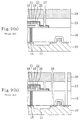
- the capacitor upper electrode 21 is exposed in the second contact hole 27 via the opening formed in the hydrogen barrier film 22 , as shown in Figure 10(a) .
- Figure 10(a) shows the state in which the second resist pattern 30 is formed on the second protective insulating film 23
- the capacitor upper electrode 21 is also opposed to the first resist pattern 29 via the opening formed in the hydrogen barrier film 22 even if the second contact hole 27 is formed in the second protective insulating film 23 by using the first resist pattern 29 .
- the active hydrogen generated on the surface of the capacitor upper electrode 21 is diffused in the capacitor upper electrode 21 through the opening of the hydrogen barrier film 22 of the capacitor upper electrode 22 to reach the capacitor insulating film 19 and reduce the insulating metal oxide composing the capacitor insulating film 19 , as shown in Figure 10(c) , which degrades the properties of the capacitor.
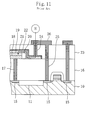
- the wiring layer 26 formed by patterning the conductive film deposited on the second protective insulating film 23 is subjected to an annealing process (sintering) performed in a hydrogen atmosphere, a hydrogen atom is diffused in the second contact plug 24 and in the capacitor upper electrode 21 to reach the capacitor insulating film 19 and reduce the insulating metal oxide composing the capacitor insulating film 19 , as shown in Figure 11 , which also degrades the properties of the capacitor.
- a semiconductor device comprises: a protective insulating film deposited on a semiconductor substrate having first and second field-effect transistors formed thereon; a capacitor composed of a capacitor lower electrode, a capacitor insulating film made of an insulating metal oxide, and a capacitor upper electrode which are formed in upwardly stacked relationship on the protective insulating film; a first contact plug formed in the protective insulating film to provide a direct connection between an impurity diffusion layer serving as a source or drain region of the first field-effect transistor and the capacitor lower electrode; and a second contact plug formed in the protective insulating film to provide a direct connection between an impurity diffusion layer serving as a source or drain region of the second field-effect transistor and the capacitor upper electrode.
- the capacitor upper electrode of the capacitor is connected directly to the impurity diffusion layer of the second field-effect transistor by the second contact plug formed in the protective insulating film, not by the wiring layer formed on the protective insulating film deposited on the capacitor as in the conventional semiconductor device.
- This obviates the necessity to form a contact hole for providing a connection between the wiring layer formed on the protective insulating film on the capacitor and the capacitor upper electrode and hence the necessity for a resist pattern for forming the contact hole.
- the capacitor upper electrode is covered with the protective insulating film on the capacitor during the formation of the contact hole for providing a connection between the wiring layer formed on the protective insulating film on the capacitor and the impurity diffusion layer of the second field-effect transistor, there can be circumvented a situation in which hydrogen generated in removing the resist pattern for forming the contact hole by using an oxygen plasma reaches the capacitor insulating film. Even if the wiring layer formed on the protective insulating film on the capacitor is treated with heat in a hydrogen atmosphere, hydrogen in the hydrogen atmosphere is prevented from reaching the capacitor insulating film since the wiring layer is not connected to the capacitor upper electrode. This prevents the reduction of the insulating metal oxide composing the capacitor insulating film and improves the properties of the capacitor.
- the capacitor insulating film is preferably formed conformally to the capacitor lower electrode, the semiconductor device preferably further comprising: insulating sidewalls formed on respective side surfaces of the capacitor lower electrode and the capacitor insulating film, wherein the capacitor upper electrode is preferably formed over the capacitor insulating film and the sidewalls.
- the insulating metal oxide film serving as the capacitor insulating film it is sufficient for the insulating metal oxide film serving as the capacitor insulating film to be formed excellently over an upper portion of the capacitor lower electrode having a flat configuration, so that the insulating metal oxide film is formed easily.
- the sidewalls are preferably made of silicon oxide.
- the capacitor lower electrode preferably includes a plurality of capacitor lower electrodes formed on the protective insulating film, the semiconductor device preferably further comprising: an insulating film formed between the plurality of capacitor lower electrodes, wherein the capacitor insulating film is preferably formed over the plurality of capacitor lower electrodes and the insulating film.
- the insulating metal oxide film serving as the capacitor insulating film is formed over the plurality of capacitor lower electrodes and the insulating film having a flat configuration, so that the insulating metal oxide film is formed easily.
- the insulating film is preferably composed of silicon oxide.
- the semiconductor device according to the present invention preferably further comprises: a hydrogen barrier film entirely covering the capacitor upper electrode.
- the arrangement positively prevents a situation in which a hydrogen atom is diffused in the capacitor upper electrode to reach the capacitor insulating film and reduce the insulating metal oxide film composing the capacitor insulating film.
- each of the first and second contact plugs is preferably made of polysilicon or tungsten.
- the capacitor insulating film is preferably made of a ferroelectric material having a bismuth layered perovskite structure, lead zirconate titanate (PZT), barium strontium titanate, or tantalum pentaoxide.
- a method of fabricating a semiconductor device comprises the steps of: depositing a protective insulating film on a semiconductor substrate having first and second field-effect transistors formed thereon; forming a first contact plug and a second contact plug in the protective insulating film, the first contact plug being connected to an impurity diffusion layer serving as a source or drain region of the first field-effect transistor, the second contact plug being connected to an impurity diffusion layer serving as a source or drain region of the second field-effect transistor; forming, on the protective insulating film, a capacitor lower electrode connected directly to the first contact plug; forming, on the capacitor lower electrode, a capacitor insulating film made of an insulating metal oxide; and forming, on the capacitor insulating film, a capacitor upper electrode having a peripheral portion located on the protective insulating film and connected directly to the second contact plug.
- the capacitor upper electrode of the capacitor is connected directly to the impurity diffusion layer of the second field-effect transistor by the second contact plug formed in the protective insulating film, not by the wiring layer formed on the protective insulating film deposited on the capacitor as in the conventional semiconductor device.
- This obviates the necessity to form a contact hole for providing a connection between the wiring layer formed on the protective insulating film on the capacitor and the capacitor upper electrode and therefore the necessity for a resist pattern for forming the contact hole.
- the capacitor upper electrode is covered with the protective insulating film on the capacitor during the formation of the contact hole for providing a connection between the wiring layer formed on the protective insulating film on the capacitor and the impurity diffusion layer of the second field-effect transistor, there can be circumvented a situation in which hydrogen generated in removing the resist pattern for forming the contact hole by using an oxygen plasma reaches the capacitor insulating film. Even if the wiring layer formed on the protective insulating film on the capacitor is treated with heat in a hydrogen atmosphere, hydrogen in the hydrogen atmosphere is prevented from reaching the capacitor insulating film since the wiring layer is not connected to the capacitor upper electrode. This prevents the reduction of the insulating metal oxide composing the capacitor insulating film and improves the properties of the capacitor.
- the method of fabricating a semiconductor device according to the present invention preferably further comprises the step of: forming a hydrogen barrier film covering the capacitor upper electrode.
- the arrangement positively prevents a situation in which a hydrogen atom is diffused in the capacitor upper electrode to reach the capacitor insulating film and reduce the insulating metal oxide composing the capacitor insulating film.
- the step of forming the capacitor insulating film preferably includes the step of forming a capacitor insulating film which is conformal to the capacitor lower electrode, the method preferably further comprising, between the step of forming the capacitor insulating film and the step of forming the capacitor upper electrode, the step of: forming insulating sidewalls on respective side surfaces of the capacitor lower electrode and the capacitor insulating film, wherein the step of forming the capacitor upper electrode preferably includes the step of forming the capacitor upper electrode over the capacitor insulating film and the sidewalls.
- the insulating metal oxide film serving as the capacitor insulating film it is sufficient for the insulating metal oxide film serving as the capacitor insulating film to be formed excellently over an upper portion of the capacitor lower electrode having a flat configuration, so that the insulating metal oxide film is formed easily.
- the step of forming the capacitor lower electrode preferably includes the step of forming a plurality of capacitor lower electrodes on the protective insulating film, the method preferably further comprising, between the step of forming the capacitor lower electrode and the step of forming the capacitor insulating film, the step of: forming an insulating film between the plurality of capacitor lower electrodes, wherein the step of forming the capacitor insulating film preferably includes the step of forming the capacitor insulating film over the plurality of capacitor lower electrodes and the insulating film.
- the insulating metal oxide film serving as the capacitor insulating film is formed over the plurality of capacitor lower electrodes and the insulating film having a flat configuration, so that the insulating metal oxide film is formed easily.
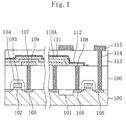
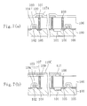
- a semiconductor device according to a first embodiment of the present invention will be described with reference to Figure 1 .
- a device isolation region 101 and impurity diffusion layers 105 each serving as the source or drain region of a first field-effect transistor or the source or drain region of the second field-effect transistor are formed in a surface portion of a semiconductor substrate 100 .
- a gate electrode 103 is formed on the semiconductor substrate 100 to be located between the pair of impurity diffusion layers 105 with a gate insulating film 102 interposed therebetween. The top and side surfaces of the gate electrode 103 are covered with a gate protective insulating film 104 .
- a first protective insulating film 106 is deposited over the gate protective insulating film 104 and the semiconductor substrate 100 .
- first and second contact plugs 107 and 108 each composed of a tungsten or polysilicon film.
- the first contact plug 107 is connected to one of the impurity diffusion layers 105 which serves as the source or drain region of the first field-effect transistor forming a memory cell and a second contact plug 108 is connected to one of the impurity diffusion layers 105 which serves as the source or drain region of the second field-effect transistor forming a sense amp.
- a plurality of capacitor lower electrodes 109 each composed of a multilayer film consisting of a titanium film, a titanium nitride film, an iridium oxide film, and a platinum film and connected to the first contact plug 107 are formed on the first protective insulating film 106 .
- a capacitor insulating film 110A made of SrBi 2 (Ta 1-x Nb x )O 9 having a bismuth layered perovskite structure is formed over the plurality of capacitor lower electrodes 109 to extend to the exterior thereof.
- a capacitor upper electrode 111 composed of a multilayer film consisting of a platinum film and a titanium film or a titanium nitride film and connected to the second contact plug 108 is formed on the capacitor insulating film 110A .
- the capacitor upper electrode 111 is covered with a hydrogen barrier film 112 composed of a silicon nitride film or a boron nitride film.
- the foregoing capacitor lower electrode 109 , the capacitor insulating film 110A , and the capacitor upper electrode 111 constitute a capacitor for storing data.
- the capacitor and the first field-effect transistor constitute a memory cell.
- a plurality of memory cells constitute a memory array.
- a second protective insulating film 113 is deposited on the first protective insulating film 106 .
- a third contact plug 114 connected to the other of the impurity diffusion layers 105 serving as the source or drain region of the second field-effect transistor is formed in the first and second protective insulating films 106 and 113 .
- a wiring layer 115 connected to the third contact plug 114 is formed on the second protective insulating film 113 .
- Each of the third contact plug 114 and the wiring layer 115 is composed of a multilayer film consisting of a titanium film, a titanium nitride film, an aluminum film, and a titanium nitride film which are deposited in upwardly stacked relationship or a multilayer film consisting of a titanium film, a titanium nitride film, a tungsten film, a titanium film, a titanium nitride film, an aluminum film, and a titanium nitride film which are deposited in upwardly stacked relationship.
- the device isolation region 101 is formed in the surface portion of the semiconductor substrate 100 , followed by the gate electrode 103 formed on the semiconductor substrate 100 with the gate insulating film 102 interposed therebetween. Then, impurity ions at a low concentration are implanted by using the gate electrode 103 as a mask and the gate protective oxide insulating film 104 is formed on the top and side surfaces of the gate electrode 103 .
- impurity ions at a high concentration are implanted by using the gate electrode 103 and the gate protective insulating film 104 as a mask, whereby the impurity diffusion layers 105 each having an LDD structure and serving as the source or drain region of the first field-effect transistor or the source or drain region of the second field-effect transistor are formed.
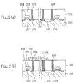
- the first protective insulating film 106 is deposited over the entire surface of the semiconductor substrate 100 and a contact hole is formed by dry etching in the first protective insulating film 106 . Then, a conductive film composed of a tungsten film or a polysilicon film is deposited by CVD over the entire surface of the first protective insulating film 106 .
- the portion of the conductive film located over the first protective insulating film 106 is removed by an etch-back or CMP process, whereby the first contact plug 107 connected to one of the impurity diffusion layers 105 which serves as the source or drain region of the first field-effect transistor forming the memory cell is formed and the second contact plug 108 connected to one of the impurity diffusion layers 105 which serves as the source or drain region of the second field-effect transistor disposed in the peripheral portion of the memory cell array to form a sense amp is formed.
- the multilayer film consisting of the titanium film, the titanium nitride film, the iridium oxide film, and the platinum film which are deposited in upwardly stacked relationship is formed over the entire surface of the first protective insulating film 106 and then patterned by dry etching, thereby forming the capacitor lower electrode 109 connected to the first contact plug 107 , as shown in Figure 2(b) .
- a ferroelectric film made of SrBi 2 (Ta 1-x Nb x )O 9 having a bismuth layered perovskite structure and having a thickness of about 100 nm to 200 nm is deposited entirely over the capacitor lower electrodes 109 and the first protective insulating film 106 by metal organic decomposition(MOD), metal organic chemical vapor deposition (MOCVD), or sputtering and then patterned, thereby forming the capacitor insulating film 110A extending over the plurality of capacitor lower electrodes 109 to the exterior thereof.
- MOD metal organic decomposition
- MOCVD metal organic chemical vapor deposition
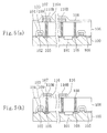
- a multilayer film consisting of a platinum film and a titanium film which are deposited in upwardly stacked relationship or a multilayer film consisting of a platinum film and a titanium nitride film which are deposited in upwardly stacked relationship is formed entirely over the capacitor insulating film 110A and the first protective film 106 and then patterned by dry etching, thereby forming the capacitor upper electrode 111 connected to the second contact plug 108 , as shown in Figure 3(a) .
- a silicon nitride film or a boron nitride film is deposited entirely over the capacitor upper electrode 111 and the first protective insulating film 106 by CVD or sputtering and then patterned by dry etching, thereby forming the hydrogen barrier film 112 covering the capacitor.
- the second protective insulating film 113 is deposited entirely over the hydrogen barrier film 112 and the first protective insulating film 106 . Then, a contact hole is formed in the second protective insulating film 113 and in the first protective insulating film 106 .
- the capacitor upper electrode 111 of the capacitor for storing data which forms the memory cell is connected directly to the impurity diffusion layer 105 of the second field-effect transistor by the second contact plug 108 formed in the first protective insulating film 106 .
- the capacitor upper electrode 111 is not connected to the impurity diffusion layer 105 via the second contact plug 24 , the wiring layer 26 , and the third contact plug 25 .
- a semiconductor device according to a second embodiment of the present invention will be described with reference to Figure 4 .
- a device isolation region 101 and impurity diffusion layers 105 each serving as the source or drain region of a first field-effect transistor or as the source or drain region of a second field-effect transistor are formed in a surface portion of a semiconductor substrate 100 , similarly to the first embodiment.
- a gate electrode 103 is formed on the semiconductor substrate 100 to be located between the pair of impurity diffusion layers 105 .
- the top and side surfaces of the gate electrode 103 are covered with the gate protective insulating film 104 .
- a first protective insulating film 106 is deposited over the semiconductor substrate 100 and the gate protective insulating film 104 .
- the first protective insulating film 106 there are formed a first contact plug 107 and a second contact plug 108 each composed of a tungsten or polysilicon film.
- the first contact plug 107 is connected to one of the impurity diffusion layers 105 which serves as the source or drain region of the first field-effect transistor forming a memory cell.
- the second contact plug 108 is connected to one of the impurity diffusion layers 105 which serves as the source or drain region of the second field-effect transistor disposed in a peripheral portion of the memory cell to serve as a sense amp.
- a capacitor lower electrode 109 composed of a multilayer film consisting of a titanium film, a titanium nitride film, an iridium oxide film, and a platinum film and connected to the first contact plug 107 is formed on the first protective insulating film 106 .
- a capacitor insulating film 110B made of SrBi 2 (Ta 1-x Nb x )O 9 having a bismuth layered perovskite structure and conformal to the capacitor lower electrode 109 is formed on the capacitor lower electrode 109 .
- the capacitor lower electrode 109 and the capacitor insulating film 110B have respective side surfaces covered with sidewalls 116 composed of a silicon oxide film.
- a capacitor upper electrode 111 composed of a multilayer film consisting of a platinum film and a titanium film or a titanium nitride film is formed over the plurality of capacitor lower electrodes 109 and the capacitor insulating film 110B to extend to the exterior thereof and connected to the second contact plug 108 .
- the capacitor upper electrode 111 is covered with a hydrogen barrier film 112 composed of a silicon nitride film or a boron nitride film.
- the foregoing capacitor lower electrode 109 , the capacitor insulating film 110B , and the capacitor upper electrode 111 constitute a capacitor for storing data.
- the capacitor and the first field-effect transistor constitute a memory cell.
- a plurality of memory cells constitute a memory array.
- a second protective insulating film 113 is deposited on the first protective insulating film 106 .
- a third contact plug 114 connected to the other of the impurity diffusion layers 105 which serves as the source or drain region of the second field-effect transistor is formed in the first and second protective insulating films 106 and 113 .
- a wiring layer 115 connected to the third contact plug 114 is formed on the second protective insulating film 113 .
- Each of the third contact plug 114 and the wiring layer 115 is composed of a multilayer film consisting of a titanium film, a titanium nitride film, an aluminum film, and a titanium nitride film which are deposited in upwardly stacked relationship or a multilayer film consisting of a titanium film, a titanium nitride film, a tungsten film, a titanium film, a titanium nitride film, an aluminum film, and a titanium nitride film which are deposited in upwardly stacked relationship.
- the device isolation region 101 is formed in the surface portion of the semiconductor substrate 100 , followed by the gate electrode 103 formed on the semiconductor substrate 100 with the gate insulating film 102 interposed therebetween and the gate protective insulating film 104 formed over the gate electrode 103 .
- the impurity diffusion layers 105 each serving as the source or drain region of the first field-effect transistor or as the source or drain region of the second field-effect transistor and having an LDD structure are formed.
- the first protective insulating film 106 is deposited over the entire surface of the semiconductor substrate 100 .
- the first contact plug 107 connected to one of the impurity diffusion layers 105 which serves as the source or drain region of the first field-effect transistor forming the memory cell is formed in the first protective insulating film
- the second contact plug 108 connected to one of the impurity diffusion layers 105 which serves as the source or drain region of the second field-effect transistor forming the sense amp is formed in the first protective insulating film 106 .
- a multilayer film consisting of a titanium film, a titanium nitride film, an iridium oxide film, and a platinum film which are deposited in upwardly stacked relationship is formed by sputtering over the entire surface of the first protective insulating film 106 .
- a ferroelectric film made of SrBi 2 (Ta 1-x Nb x )O 9 having a bismuth layered perovskite structure and having a thickness of 100 nm to 200 nm is deposited on the multilayer film by metal organic decomposition, metal organic chemical vapor deposition, or sputtering.
- the multilayer film and the ferroelectric film are patterned by dry etching to form the capacitor lower electrode 109 composed of the multilayer film and the capacitor insulating film 110B composed of the ferroelectric film.
- the silicon oxide film 108 having a thickness of 300 nm is deposited entirely over the capacitor lower electrode 109 and the capacitor insulating film 110B and subjected to anisotropic etching, thereby forming the sidewalls 116 on the respective side surfaces of the capacitor lower electrode 109 and the capacitor insulating film 110B , as shown in Figure 5(b) .
- a multilayer film consisting of a platinum film and a titanium film which are deposited in upwardly stacked relationship or a multilayer film consisting of a platinum film and a titanium nitride film which are deposited in upwardly stacked relationship is deposited over the capacitor insulating film and the first protective film 106 , similarly to the first embodiment.
- the multilayer film is patterned by dry etching, thereby forming the capacitor upper electrode 111 (see Figure 4 ) connected to the second contact plug 108 and then forming the hydrogen barrier film 112 (see Figure 4 ) covering the capacitor upper electrode 111 .
- the second protective insulating film 113 is deposited over the hydrogen barrier film 112 and the first protective insulating film 106 .
- the third contact plug 114 (see Figure 4 ) connected to the other of the impurity diffusion layers 105 which serves as the source or drain region of the second field-effect transistor is formed in the first and second protective insulating films 106 and 113 , while the wiring layer 115 (see Figure 4 ) connected to the third contact plug 114 is formed on the second protective insulating film 113 .
- the capacitor upper electrode 111 of the capacitor for storing data which forms the memory cell is connected directly to the impurity diffusion layer 105 of the second field-effect transistor by the second contact plug 108 formed in the first protective insulating film 106 . Since an opening is not formed in the hydrogen barrier film 112 covering the capacitor lower electrode 111 , there can be circumvented a situation in which active hydrogen generated by the catalytic reaction of platinum and a hydrogen atom in a hydrogen atmosphere in which the wiring layer 115 is annealed are diffused in the capacitor upper electrode 111 to reach the capacitor insulating film 110A . Accordingly, the capacitor insulating film 110A is not reduced by hydrogen and the properties of the capacitor are improved.
- the second embodiment has deposited the ferroelectric film serving as the capacitor insulating film 110B on the multilayer film serving as the capacitor lower electrode 109 , i.e., the second embodiment has deposited the ferroelectric film on the flat multilayer film. This allows easy formation of the ferroelectric film.
- the multilayer film serving as the capacitor upper electrode 111 is deposited after the sidewalls 116 are formed on the respective side surfaces of the capacitor lower electrode 109 and the capacitor insulating film 110B , there is no conduction between the capacitor lower electrodes 109 .
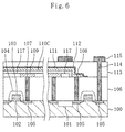
- a device isolation region 101 and impurity diffusion layers 105 each serving as the source or drain region of a first field-effect transistor or as the source or drain region of a second field-effect transistor are formed in a surface portion of a semiconductor substrate 100 , similarly to the first embodiment.
- a gate electrode 103 is formed on the semiconductor substrate 100 to be located between the pair of impurity diffusion layers 105 .
- the top and side surfaces of the gate electrode 103 are covered with the gate protective insulating film 104 .
- a first protective insulating film 106 is deposited over the semiconductor substrate 100 and the gate protective insulating film 104 .
- the first protective insulating film 106 there are formed a first contact plug 107 and a second contact plug 108 each composed of a tungsten or polysilicon film.
- the first contact plug 107 is connected to one of the impurity diffusion layers 105 which serves as the source or drain region of the first field-effect transistor forming a memory cell.
- the second contact plug 108 is connected to one of the impurity diffusion layers 105 which serves as the source or drain region of the second field-effect transistor disposed in a peripheral portion of the memory cell to serve as a sense amp.
- a capacitor lower electrode 109 composed of a multilayer film consisting of a titanium film, a titanium nitride film, an iridium oxide film, and a platinum film and connected to the first contact plug 107 is formed on the first protective insulating film 106 .
- An insulating film 117 composed of a silicon oxide film is formed on the first protective insulating film 106 to be located between the capacitor lower electrodes 109 .
- a capacitor insulating film 110C made of SrBi 2 (Ta 1-x Nb x )O 9 having a bismuth layered perovskite structure is formed over the plurality of capacitor lower electrodes 109 and the insulating film 117 to extend to the exterior thereof.
- a capacitor upper electrode 111 composed of a multilayer film consisting of a platinum film and a titanium film or a titanium nitride film and connected to the second contact plug 108 is formed on the capacitor insulating film 110C to extend to the exterior thereof.
- the capacitor upper electrode 111 is covered with a hydrogen barrier film 112 composed of a silicon nitride film or a boron nitride film.
- the foregoing capacitor lower electrode 109 , the capacitor insulating film 110C , and the capacitor upper electrode 111 constitute a capacitor for storing data.
- the capacitor and the first field-effect transistor constitute a memory cell.
- a plurality of memory cells constitute a memory array.
- a second protective insulating film 113 is deposited on the first protective insulating film 106 .
- a third contact plug 114 connected to the other of the impurity diffusion layers 105 which serves as the source or drain region of the second field-effect transistor is formed in the first and second protective insulating films 106 and 113 .
- a wiring layer 115 connected to the third contact plug 114 is formed on the second protective insulating film 113 .
- Each of the third contact plug 114 and the wiring layer 115 is composed of a multilayer film consisting of a titanium film, a titanium nitride film, an aluminum film, and a titanium nitride film which are deposited in upwardly stacked relationship or a multilayer film consisting of a titanium film, a titanium nitride film, a tungsten film, a titanium film, a titanium nitride film, an aluminum film, and a titanium nitride film which are deposited in upwardly stacked relationship.
- the device isolation region 101 is formed in the surface portion of the semiconductor substrate 100 , followed by the gate electrode 103 formed on the semiconductor substrate 100 with the gate insulating film 102 interposed therebetween and the gate protective insulating film 104 formed over the gate electrode 103 .
- the impurity diffusion layers 105 each serving as the source or drain region of the first field-effect transistor or as the source or drain region of the second field-effect transistor and having an LDD structure are formed.
- the first protective insulating film 106 is deposited over the entire surface of the semiconductor substrate 100 .
- the first contact plug 107 connected to one of the impurity diffusion layers 105 which serves as the source or drain region of the first field-effect transistor forming the memory cell is formed in the first protective insulating film
- the second contact plug 108 connected to one of the impurity diffusion layers 105 which serves as the source or drain region of the second field-effect transistor forming the sense amp is formed in the first protective insulating film 106 .
- a multilayer film consisting of a titanium film, a titanium nitride film, an iridium oxide film, and a platinum film which are deposited in upwardly stacked relationship is formed by sputtering over the entire surface of the first protective insulating film 106 .
- the multilayer film is then patterned by dry etching, thereby forming the capacitor lower electrode 109 .
- a silicon oxide film 117A having a thickness of 300 nm is deposited over the entire surface of the capacitor lower electrode 109 .
- the portion of the silicon oxide film 117A overlying the capacitor lower electrode 109 is removed by CMP, whereby the insulating film 117 composed of the silicon oxide film 117A is formed on the first protective insulating film 106 to be located between the capacitor lower electrodes 109 , as shown in Figure 7(b) .
- a ferroelectric film made of SrBi 2 (Ta 1-x Nb x )O 9 having a bismuth layered perovskite structure and having a thickness of 100 nm to 200 nm is deposited over the plurality of capacitor lower electrodes 109 and the insulating film 117 by metal organic decomposition, metal organic chemical vapor deposition, or sputtering.
- the ferroelectric film is then patterned by dry etching to form the capacitor insulating film 110C extending over the plurality of capacitor lower electrodes 109 to the exterior thereof.
- a multilayer film consisting of a platinum film and a titanium film which are deposited in upwardly stacked relationship or a multilayer film consisting of a platinum film and a titanium nitride film which are deposited in upwardly stacked relationship is deposited over the capacitor insulating film and the first protective film 106 , similarly to the first embodiment.
- the multilayer film is patterned by dry etching, thereby forming the capacitor upper electrode 111 (see Figure 6 ) connected to the second contact plug 108 and then forming the hydrogen barrier film 112 (see Figure 6 ) covering the capacitor upper electrode 111 .
- the second protective insulating film 113 is deposited over the hydrogen barrier film 112 and the first protective insulating film 106 .
- the third contact plug 114 (see Figure 6 ) connected to the other of the impurity diffusion layers 105 which serves as the source or drain region of the second field-effect transistor is formed in the first and second protective insulating films 106 and 113 , while the wiring layer 115 (see Figure 6 ) connected to the third contact plug 114 is formed on the second protective insulating film 113 .
- the capacitor upper electrode 111 of the capacitor for storing data which forms the memory cell is connected directly to the impurity diffusion layer 105 of the second field-effect transistor by the second contact plug 108 formed in the first protective insulating film 106 . Since an opening is not formed in the hydrogen barrier film 112 covering the capacitor lower electrode 111 , there can be circumvented a situation in which active hydrogen generated by the catalytic reaction of platinum and a hydrogen atom in a hydrogen atmosphere in which the wiring layer 115 is annealed are diffused in the capacitor upper electrode 111 to reach the capacitor insulating film 110A . Accordingly, the capacitor insulating film 110A is not reduced by hydrogen and the properties of the capacitor are improved.
- the third embodiment has deposited the ferroelectric film serving as the capacitor insulating film 110C over the plurality of capacitor lower electrodes 109 and the insulating film 117 having their surfaces planarized. This allows easy formation of the ferroelectric film.
- each of the capacitor insulating films 110A , 110B , and 110C may also be formed of a ferroelectric film having a bismuth layered perovskite structure having another composition or of a high-dielectric-constant film such as lead zirconate titanate, barium strontium titanate, or tantalum pentaoxide.
- the capacitor upper electrode 111 has been formed of the multilayer film consisting of the platinum film and the titanium film which are deposited in upwardly stacked relationship or of the multilayer film consisting of the platinum film and the titanium nitride film which are deposited in upwardly stacked relationship, it is not limited thereto.
- the capacitor upper electrode 111 may be formed appropriately so long as it contains a platinum film, an iridium film, a ruthenium film, a rhodium film, or a multilayer film consisting of some of the films listed above.
- the capacitor lower electrode 109 has been formed of the multilayer film consisting of the titanium film, the titanium nitride film, the iridium oxide film, and the platinum film which are deposited in upwardly stacked relationship, it is not limited thereto.
- the capacitor lower electrode 109 may be formed appropriately so long as it contains a platinum film, an iridium film, a ruthenium film, a rhodium film, or a multilayer film consisting of some of the films listed above.
Landscapes
- Engineering & Computer Science (AREA)
- Manufacturing & Machinery (AREA)
- Semiconductor Memories (AREA)
- Internal Circuitry In Semiconductor Integrated Circuit Devices (AREA)
Applications Claiming Priority (2)
| Application Number | Priority Date | Filing Date | Title |
|---|---|---|---|
| JP14610399 | 1999-05-26 | ||
| JP14610399 | 1999-05-26 |
Publications (2)
| Publication Number | Publication Date |
|---|---|
| EP1056128A2 true EP1056128A2 (fr) | 2000-11-29 |
| EP1056128A3 EP1056128A3 (fr) | 2003-12-03 |
Family
ID=15400225
Family Applications (1)
| Application Number | Title | Priority Date | Filing Date |
|---|---|---|---|
| EP00111276A Withdrawn EP1056128A3 (fr) | 1999-05-26 | 2000-05-25 | Dispositif semi-conducteur à mémoire et son procédé de manufacture |
Country Status (6)
| Country | Link |
|---|---|
| US (5) | US6441420B1 (fr) |
| EP (1) | EP1056128A3 (fr) |
| JP (2) | JP3759859B2 (fr) |
| KR (1) | KR100522211B1 (fr) |
| CN (1) | CN1170316C (fr) |
| TW (1) | TW454330B (fr) |
Cited By (5)
| Publication number | Priority date | Publication date | Assignee | Title |
|---|---|---|---|---|
| EP1204142A2 (fr) | 2000-10-17 | 2002-05-08 | Matsushita Electric Industrial Co., Ltd. | Mémoire ferroélectrique et son procédé de manufacture |
| KR100395766B1 (ko) * | 2001-02-12 | 2003-08-25 | 삼성전자주식회사 | 강유전체 기억 소자 및 그 형성 방법 |
| EP1351253A1 (fr) * | 2002-04-02 | 2003-10-08 | Hewlett-Packard Company | Structures de mémoire |
| US7485935B2 (en) | 2006-04-25 | 2009-02-03 | Panasonic Corporation | Semiconductor memory device |
| US8624214B2 (en) | 2008-06-10 | 2014-01-07 | Panasonic Corporation | Semiconductor device having a resistance variable element and a manufacturing method thereof |
Families Citing this family (36)
| Publication number | Priority date | Publication date | Assignee | Title |
|---|---|---|---|---|
| JP4829678B2 (ja) * | 2000-10-17 | 2011-12-07 | パナソニック株式会社 | 強誘電体メモリ及びその製造方法 |
| JP3833887B2 (ja) * | 2000-10-30 | 2006-10-18 | 株式会社東芝 | 強誘電体メモリ及びその製造方法 |
| KR20020082549A (ko) * | 2001-04-24 | 2002-10-31 | 주식회사 하이닉스반도체 | 고용량 엠아이엠 캐패시터 제조방법 |
| US6730951B2 (en) | 2001-06-25 | 2004-05-04 | Matsushita Electric Industrial Co., Ltd. | Capacitor, semiconductor memory device, and method for manufacturing the same |
| EP1298730A3 (fr) * | 2001-09-27 | 2007-12-26 | Matsushita Electric Industrial Co., Ltd. | Mémoire ferroélectrique et son procédé de fabrication |
| JP4368085B2 (ja) | 2002-01-08 | 2009-11-18 | 富士通マイクロエレクトロニクス株式会社 | 半導体装置の製造方法 |
| KR100450669B1 (ko) * | 2002-01-30 | 2004-10-01 | 삼성전자주식회사 | 산소 침투 경로 및 캡슐화 장벽막을 구비하는 강유전체메모리 소자 및 그 제조 방법 |
| JP2004146772A (ja) * | 2002-03-18 | 2004-05-20 | Fujitsu Ltd | 半導体装置及びその製造方法 |
| JP4316188B2 (ja) | 2002-05-29 | 2009-08-19 | 富士通マイクロエレクトロニクス株式会社 | 半導体装置及びその製造方法 |
| JP4507532B2 (ja) * | 2002-08-27 | 2010-07-21 | 日亜化学工業株式会社 | 窒化物半導体素子 |
| KR100480641B1 (ko) * | 2002-10-17 | 2005-03-31 | 삼성전자주식회사 | 고 커패시턴스를 지니는 금속-절연체-금속 커패시터, 이를구비하는 집적회로 칩 및 이의 제조 방법 |
| US7229875B2 (en) * | 2002-10-17 | 2007-06-12 | Samsung Electronics Co., Ltd. | Integrated circuit capacitor structure |
| US7297558B2 (en) | 2003-04-03 | 2007-11-20 | Fujitsu Limited | Method of manufacturing semiconductor device |
| US6913965B2 (en) * | 2003-06-12 | 2005-07-05 | International Busniess Machines Corporation | Non-Continuous encapsulation layer for MIM capacitor |
| TWI228807B (en) * | 2003-07-01 | 2005-03-01 | Advanced Semiconductor Eng | Wafer level passive component |
| KR20050033672A (ko) * | 2003-10-07 | 2005-04-13 | 삼성전자주식회사 | 커패시터-언더-비트라인 구조의 반도체 장치 및 이의 제조방법 |
| JP4316358B2 (ja) * | 2003-11-27 | 2009-08-19 | 株式会社東芝 | 半導体記憶装置及びその製造方法 |
| JP3810411B2 (ja) * | 2004-01-23 | 2006-08-16 | Necエレクトロニクス株式会社 | 集積回路装置 |
| JP4541717B2 (ja) * | 2004-02-09 | 2010-09-08 | ルネサスエレクトロニクス株式会社 | 集積回路装置及びその製造方法 |
| JP3935475B2 (ja) | 2004-03-18 | 2007-06-20 | 松下電器産業株式会社 | 半導体装置及びその製造方法 |
| US7580241B2 (en) * | 2004-04-26 | 2009-08-25 | Tdk Corporation | Thin film capacitor element composition, high permittivity insulation film, thin film capacitor element, thin film multilayer capacitor, and method of production of thin film capacitor element |
| US6906908B1 (en) | 2004-05-20 | 2005-06-14 | Kabushiki Kaisha Toshiba | Semiconductor device and method of manufacturing the same |
| JP4025316B2 (ja) | 2004-06-09 | 2007-12-19 | 株式会社東芝 | 半導体装置の製造方法 |
| JP2006302987A (ja) * | 2005-04-18 | 2006-11-02 | Nec Electronics Corp | 半導体装置およびその製造方法 |
| KR100735521B1 (ko) * | 2005-10-19 | 2007-07-04 | 삼성전자주식회사 | 반도체 소자 및 그 제조 방법 |
| JP2007150025A (ja) * | 2005-11-29 | 2007-06-14 | Seiko Epson Corp | 強誘電体メモリの製造方法 |
| DE602007008841D1 (de) * | 2006-02-10 | 2010-10-14 | Nxp Bv | Halbleiterbauelement und verfahren zu seiner herstellung |
| JP4557903B2 (ja) * | 2006-02-10 | 2010-10-06 | パナソニック株式会社 | 半導体装置及びその製造方法 |
| CN100479162C (zh) * | 2006-04-24 | 2009-04-15 | 联华电子股份有限公司 | 半导体元件及其制造方法 |
| JP2008108761A (ja) | 2006-10-23 | 2008-05-08 | Elpida Memory Inc | ダイナミックランダムアクセスメモリの製造方法 |
| KR100823168B1 (ko) * | 2007-01-08 | 2008-04-18 | 삼성전자주식회사 | 강유전체 메모리 장치 및 그 형성 방법 |
| US7592273B2 (en) * | 2007-04-19 | 2009-09-22 | Freescale Semiconductor, Inc. | Semiconductor device with hydrogen barrier and method therefor |
| JP5292878B2 (ja) * | 2008-03-26 | 2013-09-18 | 富士通セミコンダクター株式会社 | 半導体装置の製造方法 |
| US20100224960A1 (en) * | 2009-03-04 | 2010-09-09 | Kevin John Fischer | Embedded capacitor device and methods of fabrication |
| JP5327139B2 (ja) * | 2010-05-31 | 2013-10-30 | 富士通セミコンダクター株式会社 | 半導体装置及びその製造方法 |
| JP6336826B2 (ja) * | 2014-06-04 | 2018-06-06 | ルネサスエレクトロニクス株式会社 | 半導体装置 |
Family Cites Families (24)
| Publication number | Priority date | Publication date | Assignee | Title |
|---|---|---|---|---|
| US5276344A (en) * | 1990-04-27 | 1994-01-04 | Mitsubishi Denki Kabushiki Kaisha | Field effect transistor having impurity regions of different depths and manufacturing method thereof |
| JPH04298030A (ja) * | 1991-03-27 | 1992-10-21 | Sony Corp | メタルプラグの形成方法 |
| JP3197064B2 (ja) | 1992-07-17 | 2001-08-13 | 株式会社東芝 | 半導体記憶装置 |
| JPH0685193A (ja) | 1992-09-07 | 1994-03-25 | Nec Corp | 半導体装置 |
| JP3212194B2 (ja) | 1992-09-11 | 2001-09-25 | 株式会社東芝 | 半導体装置の製造方法 |
| JP3161836B2 (ja) * | 1992-10-19 | 2001-04-25 | シャープ株式会社 | 半導体記憶装置 |
| JPH0783061B2 (ja) * | 1993-01-05 | 1995-09-06 | 日本電気株式会社 | 半導体装置 |
| US5335138A (en) * | 1993-02-12 | 1994-08-02 | Micron Semiconductor, Inc. | High dielectric constant capacitor and method of manufacture |
| JPH0794600A (ja) | 1993-06-29 | 1995-04-07 | Mitsubishi Electric Corp | 半導体装置およびその製造方法 |
| US5644151A (en) * | 1994-05-27 | 1997-07-01 | Nippon Steel Corporation | Semiconductor memory device and method for fabricating the same |
| US5563762A (en) * | 1994-11-28 | 1996-10-08 | Northern Telecom Limited | Capacitor for an integrated circuit and method of formation thereof, and a method of adding on-chip capacitors to an integrated circuit |
| US5567636A (en) * | 1995-02-27 | 1996-10-22 | Motorola Inc. | Process for forming a nonvolatile random access memory array |
| JP3417167B2 (ja) * | 1995-09-29 | 2003-06-16 | ソニー株式会社 | 半導体メモリ素子のキャパシタ構造及びその形成方法 |
| US5843830A (en) * | 1996-06-26 | 1998-12-01 | Micron Technology, Inc. | Capacitor, and methods for forming a capacitor |
| US5880991A (en) * | 1997-04-14 | 1999-03-09 | International Business Machines Corporation | Structure for low cost mixed memory integration, new NVRAM structure, and process for forming the mixed memory and NVRAM structure |
| JPH10340871A (ja) | 1997-06-06 | 1998-12-22 | Toshiba Corp | 研磨方法及び半導体装置の製造方法 |
| JPH118355A (ja) | 1997-06-16 | 1999-01-12 | Nec Corp | 強誘電体メモリ |
| JP3090198B2 (ja) | 1997-08-21 | 2000-09-18 | 日本電気株式会社 | 半導体装置の構造およびその製造方法 |
| JPH11126881A (ja) | 1997-10-23 | 1999-05-11 | Hitachi Ltd | 高強誘電体薄膜コンデンサを有する半導体装置及びその製造方法 |
| JP3098474B2 (ja) * | 1997-10-31 | 2000-10-16 | 日本電気株式会社 | 半導体装置の製造方法 |
| US6509601B1 (en) * | 1998-07-31 | 2003-01-21 | Samsung Electronics Co., Ltd. | Semiconductor memory device having capacitor protection layer and method for manufacturing the same |
| US6249014B1 (en) | 1998-10-01 | 2001-06-19 | Ramtron International Corporation | Hydrogen barrier encapsulation techniques for the control of hydrogen induced degradation of ferroelectric capacitors in conjunction with multilevel metal processing for non-volatile integrated circuit memory devices |
| US6121648A (en) * | 1999-03-31 | 2000-09-19 | Radiant Technologies, Inc | Ferroelectric based memory devices utilizing hydrogen getters and recovery annealing |
| US6242299B1 (en) * | 1999-04-01 | 2001-06-05 | Ramtron International Corporation | Barrier layer to protect a ferroelectric capacitor after contact has been made to the capacitor electrode |
-
2000
- 2000-05-16 TW TW089109360A patent/TW454330B/zh not_active IP Right Cessation
- 2000-05-19 CN CNB001062514A patent/CN1170316C/zh not_active Expired - Fee Related
- 2000-05-24 US US09/576,971 patent/US6441420B1/en not_active Ceased
- 2000-05-24 JP JP2000152324A patent/JP3759859B2/ja not_active Expired - Lifetime
- 2000-05-25 EP EP00111276A patent/EP1056128A3/fr not_active Withdrawn
- 2000-05-26 KR KR10-2000-0028573A patent/KR100522211B1/ko not_active Expired - Fee Related
-
2002
- 2002-06-10 US US10/164,409 patent/US6756282B2/en not_active Expired - Lifetime
-
2004
- 2004-04-22 US US10/829,476 patent/USRE41625E1/en not_active Expired - Lifetime
- 2004-06-22 US US10/872,561 patent/US20040229429A1/en not_active Abandoned
-
2005
- 2005-06-09 JP JP2005169556A patent/JP2005277443A/ja active Pending
- 2005-11-10 US US11/270,615 patent/US7531863B2/en not_active Expired - Lifetime
Cited By (6)
| Publication number | Priority date | Publication date | Assignee | Title |
|---|---|---|---|---|
| EP1204142A2 (fr) | 2000-10-17 | 2002-05-08 | Matsushita Electric Industrial Co., Ltd. | Mémoire ferroélectrique et son procédé de manufacture |
| EP1204142A3 (fr) * | 2000-10-17 | 2009-01-14 | Panasonic Corporation | Mémoire ferroélectrique et son procédé de manufacture |
| KR100395766B1 (ko) * | 2001-02-12 | 2003-08-25 | 삼성전자주식회사 | 강유전체 기억 소자 및 그 형성 방법 |
| EP1351253A1 (fr) * | 2002-04-02 | 2003-10-08 | Hewlett-Packard Company | Structures de mémoire |
| US7485935B2 (en) | 2006-04-25 | 2009-02-03 | Panasonic Corporation | Semiconductor memory device |
| US8624214B2 (en) | 2008-06-10 | 2014-01-07 | Panasonic Corporation | Semiconductor device having a resistance variable element and a manufacturing method thereof |
Also Published As
| Publication number | Publication date |
|---|---|
| KR100522211B1 (ko) | 2005-10-14 |
| US6756282B2 (en) | 2004-06-29 |
| US20040229429A1 (en) | 2004-11-18 |
| USRE41625E1 (en) | 2010-09-07 |
| TW454330B (en) | 2001-09-11 |
| US6441420B1 (en) | 2002-08-27 |
| CN1170316C (zh) | 2004-10-06 |
| US20060065918A1 (en) | 2006-03-30 |
| JP3759859B2 (ja) | 2006-03-29 |
| JP2001044376A (ja) | 2001-02-16 |
| EP1056128A3 (fr) | 2003-12-03 |
| JP2005277443A (ja) | 2005-10-06 |
| US7531863B2 (en) | 2009-05-12 |
| CN1275808A (zh) | 2000-12-06 |
| KR20010020905A (ko) | 2001-03-15 |
| US20020149045A1 (en) | 2002-10-17 |
Similar Documents
| Publication | Publication Date | Title |
|---|---|---|
| US6756282B2 (en) | Semiconductor device and method of fabricating the same | |
| US6730951B2 (en) | Capacitor, semiconductor memory device, and method for manufacturing the same | |
| US8236643B2 (en) | Method of manufacturing semiconductor device including ferroelectric capacitor | |
| US6605835B2 (en) | Ferroelectric memory and its method of fabrication | |
| US20140017819A1 (en) | Semiconductor device and method of manufacturing the same | |
| JP2005057103A (ja) | 半導体装置及びその製造方法 | |
| JP3643091B2 (ja) | 半導体記憶装置及びその製造方法 | |
| US20020042185A1 (en) | Semiconductor integrated circuit device and manufacturing method thereof | |
| US7052951B2 (en) | Ferroelectric memory devices with enhanced ferroelectric properties and methods for fabricating such memory devices | |
| US20010015451A1 (en) | Semiconductor memory device | |
| KR100973703B1 (ko) | 반도체 장치 및 그 제조 방법 | |
| US20040000687A1 (en) | Ferroelectric capacitors with metal oxide for inhibiting fatigue and methods of forming the same | |
| US7501675B2 (en) | Semiconductor device and method of manufacturing the same | |
| JP4002882B2 (ja) | 容量素子、半導体記憶装置及びその製造方法 | |
| EP1061582A2 (fr) | Condensateur et son procédé de fabrication | |
| JP3967315B2 (ja) | 容量素子、半導体記憶装置及びその製造方法 | |
| JP2007042705A (ja) | 半導体装置及びその製造方法 | |
| JP2008098219A (ja) | 半導体記憶装置及びその製造方法 |
Legal Events
| Date | Code | Title | Description |
|---|---|---|---|
| PUAI | Public reference made under article 153(3) epc to a published international application that has entered the european phase |
Free format text: ORIGINAL CODE: 0009012 |
|
| AK | Designated contracting states |
Kind code of ref document: A2 Designated state(s): AT BE CH CY DE DK ES FI FR GB GR IE IT LI LU MC NL PT SE |
|
| AX | Request for extension of the european patent |
Free format text: AL;LT;LV;MK;RO;SI |
|
| RAP1 | Party data changed (applicant data changed or rights of an application transferred) |
Owner name: MATSUSHITA ELECTRIC INDUSTRIAL CO., LTD. |
|
| PUAL | Search report despatched |
Free format text: ORIGINAL CODE: 0009013 |
|
| AK | Designated contracting states |
Kind code of ref document: A3 Designated state(s): AT BE CH CY DE DK ES FI FR GB GR IE IT LI LU MC NL PT SE |
|
| AX | Request for extension of the european patent |
Extension state: AL LT LV MK RO SI |
|
| 17P | Request for examination filed |
Effective date: 20040514 |
|
| AKX | Designation fees paid |
Designated state(s): DE FR NL |
|
| RAP1 | Party data changed (applicant data changed or rights of an application transferred) |
Owner name: PANASONIC CORPORATION |
|
| STAA | Information on the status of an ep patent application or granted ep patent |
Free format text: STATUS: THE APPLICATION HAS BEEN WITHDRAWN |
|
| 18W | Application withdrawn |
Effective date: 20090219 |