EP1058092A2 - Systéme d'acquisition des données - Google Patents
Systéme d'acquisition des données Download PDFInfo
- Publication number
- EP1058092A2 EP1058092A2 EP00650057A EP00650057A EP1058092A2 EP 1058092 A2 EP1058092 A2 EP 1058092A2 EP 00650057 A EP00650057 A EP 00650057A EP 00650057 A EP00650057 A EP 00650057A EP 1058092 A2 EP1058092 A2 EP 1058092A2
- Authority
- EP
- European Patent Office
- Prior art keywords
- data
- processor
- comprises means
- memory
- analog
- Prior art date
- Legal status (The legal status is an assumption and is not a legal conclusion. Google has not performed a legal analysis and makes no representation as to the accuracy of the status listed.)
- Withdrawn
Links
Images


Classifications
-
- G—PHYSICS
- G01—MEASURING; TESTING
- G01D—MEASURING NOT SPECIALLY ADAPTED FOR A SPECIFIC VARIABLE; ARRANGEMENTS FOR MEASURING TWO OR MORE VARIABLES NOT COVERED IN A SINGLE OTHER SUBCLASS; TARIFF METERING APPARATUS; MEASURING OR TESTING NOT OTHERWISE PROVIDED FOR
- G01D3/00—Indicating or recording apparatus with provision for the special purposes referred to in the subgroups
- G01D3/08—Indicating or recording apparatus with provision for the special purposes referred to in the subgroups with provision for safeguarding the apparatus, e.g. against abnormal operation, against breakdown
Definitions
- the invention relates to acquisition of data from a rotor.
- a data capture system comprising means for interfacing with transducers and means for transferring data to an external host system, characterised in that the system further comprises:
- the processor comprises means for operating in a cycle comprising a ready mode, a data capture mode, and return to a ready mode, and for initiating the cycle according to commands received from an external host.
- the processor comprises means for writing data to a mapped memory section during the ready modes and for repeatedly over-writing said memory section.
- system further comprises a low pass filter
- processor comprises means for writing only a portion of the samples to the memory and for activating said filter during the ready modes.
- the processor comprises means for writing data to the memory in a sequential pattern according to time of receipt, and for directing upload of the data in said pattern.
- the processor comprises means for writing data words to the memory in sequence, each word comprising all simultaneous data from all analog to digital converters.
- system further comprises:
- the system comprises a plurality of physically separate circuits, each comprising analog to digital converters, a processor, and a memory, each circuit being of elongate shape and comprising means for mounting within a rotor symmetrically about the rotor axis.
- system comprises a master clock source connected to all of the processors, and each processor comprises means for operating according to a high frequency clock for processor operations and according to a lower frequency clock for host interfacing operations.
- the host interface comprises a serial interface associated with each processor.
- each processor has an associated serial interfacing clock source and comprises means for synchronising the interfacing clock according to the master clock.
- each processor comprises means for operating according to state machines and the system comprises means for providing a synchronised state machine clock to all processors.
- each processor comprises means for operating according to two state machines (M1, M2), one operating at a lower frequency than the other.
- the state machine operating at the lower frequency is used for putting the analog to digital converters into standby mode, for synchronising the analog to digital converters, and for initiating a calibration cycle for the analog to digital converters.
- each processor comprises means for also using the lower frequency state machine for transmitting status data to an external host via the host interface.
- each processor comprises means for using the higher-frequency state machine to control read-back of stored data and for sending status data to a host.
- each processor comprises means for interlinking the state machines via a re-timing circuit.
- re-timing circuit comprises a D-type flip-flop.
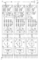
- FIG. 1 there is shown a data capture system 1 for use in a mechanical rotor system 2 having a central shaft indicated by interrupted lines and turbines, not shown.
- Signal cables 3 are connected to transducers in the system such as strain gauges.
- the mechanical system rotates about an axis 4.
- the system 1 comprises a set of three modular amplifier circuits 10 which are connected to the stain gauge cables 3.
- the amplifier circuits 10 are in turn connected to three corresponding modular data capture circuits 11.
- the data capture circuits 11 are connected by a serial link 13 to a slip ring 14 for download of data to a host system 15 and to receive commands from the host system 15.
- the mechanical system ramps up to a maximum speed of approximately 8000 rpm and at a certain point sampling is triggered by either a tachometer or the host system 15.
- a command is transmitted via the serial link 13 to the data capture circuit 11 to initiate sampling.
- Sampling involves data capture for a period of 0.2, 0.4, 0.6, or 0.8 seconds and different such periods may be chosen by the host system 15 in order to gather sufficient information for analysis of performance of the mechanical system.
- the data is stored in the data capture circuits 11 and it only downloaded subsequently. The downloads may take place as the shaft 2 is rotating, in which case the slip ring 14 is used, or it may take place when stationary.
- the cables 3 connect to a signal conditioning circuit 20 which conditions the signals to provide a linear voltage output.
- This signal is amplified by amplifiers 21 to provide a voltage output range of 0 -2.5 V over the entire bandwidth.
- each amplifier circuit 10 is to handle eight analog transducer channels and to provide conditioning and amplification channels to a corresponding data capture circuit 11.
- a data capture circuit indicated by 11 M operates as a master and the other two, indicated by 11 S, operate as slaves.
- the primary difference between the master and the slaves is that the master hosts a master clock source which provides a master clock signal for all circuits.
- each data capture circuit 11 comprises a switchable low pass filter 24 which delivers the eight analog channels to eight analog to digital converters (ADCs) 25.
- the ADCs 25 are of the type which oversample and have internal digital filters.
- the digital output of the converters 25 is fed to a processor, in this embodiment a field programmable gate array (FPGA) 26.
- FPGA 26 is connected to a serial clock source 27 providing 7.6 MHz.
- the master data capture circuit 11 M includes a master clock source 28 which delivers 10 MHz to the on-board FPGA 26 and to the FPGAs 26 of the slave circuits 11 S.
- the FPGA 26 of the master circuit 11 M also derives a 500 Hz clock signal from the master clock signal and delivers this on lines 29 to the two slave circuits 11 S.
- Each FPGA 26 is connected to two DRAM circuits 30, each of 16 Mb capacity. Each FPGA 26 is also connected to an RS 485 serial interface 31, which is in turn connected to the serial link 13 for communication with an external system via the slip ring 14.
- the filter 24 has a 500 Hz low pass filter, and for high frequency sampling the filter has an antialiasing filter to allow sampling at 312.5 k samples per second.
- the ADCs 25 are driven by the master clock at 10 MHz and new 16-bit samples are available every 32 clock periods, giving a sampling rate of 312.5k samples per second. This is just greater than twice the signal bandwidth which provides for very efficient storage/transmission. It is made possible by the use of sigma-delta analog to digital oversampling in the ADCs 25.
- Each FPGA 26 synchronises and calibrates the ADCs 25 immediately prior to a sampling phase during which the eight serial data streams are reconstructed in parallel format and stored in the memory chips 30. During sampling, the maximum number of samples stored corresponds to filling the two memory chips 30 on each circuit 11.
- Each sample includes eight channels and there are two bytes per channel providing a total of 16 bytes per sample.
- the data is written in an interleaved format as follows.
- a very important aspect of the data capture is that the three data capture circuits 11 operate in synchronism according to the 10 MHz master clock and the location in the memories 30 derives directly from the time at which the sample was received. This is because the samples are written in sequential order to the memories according to time of receipt and this pattern is mirrored in all of the memories 30 so that they operate as if they were one contiguous memory bank.
- This synchronism has been achieved by use of the master clock 28 on the master capture circuit 11 M and by directly connecting this clock to the slave capture circuits 11 S.
- the FPGA 26 of the master capture circuit 11 provides a state machine 500 Hz clock signal on the lines 29 to the two slave capture circuits 11 S. Use of this clock signal is described in more detail below.
- Each FPGA 26 performs a cycle comprising a "ready" mode (alternatively referred to as a low speed sampling (LSS) mode), a sampling mode (alternatively referred to as a high speed sampling (HSS) mode), followed again by an LSS mode.
- LSS low speed sampling
- HSS high speed sampling
- the signals to the two DRAMs 30 on each circuit 11 are common, apart from the signal CAS which effectively switches the storage (and read-out during read-back periods) from one DRAM to the other.
- CAS0 For the lower half of the address range CAS0 is active and CAS 1 is inactive. These roles are reversed for the upper half of the address range. This means that address bit 0 is used to select the active CAS.
- the LSS mode involves each FPGA filling a 32K pre-mapped section of one of the DRAMs 30 by repeatably overwriting this mapped region.
- the FPGA switches the switchable filter 24 to the low pass setting which allows it to ignore 255 of every 256 incoming samples and use them to provide the LSS mode data to the pre-mapped memory region.
- the low pass filter removes high frequencies to prevent aliasing.
- Each FPGA 26 then receives via the serial link 13 and the RS485 interface 31 a command signal from either a tachometer or from the external host system 15 to start sampling. Typically, this may arise when the rotor speed approaches a pre-set value such as after it has ramped up to 8000 rpm. When the FPGA 26 receives this signal it switches off the filter 24 and starts sampling at the full rate of all 312.5 k samples/sec. To start the HSS mode, the current value of the DRAM address is stored so that the first value read is this location (holding the oldest sample value). This address is held in a register in the FPGA 26. Also, the DRAM address must jump to the value 008000 H , the start of the HSS region.
- the FPGA 26 also switches the filter 24 from a low frequency of approximately 500 Hz (for LSS) to approximately 1 MHz for the HSS mode. Each FPGA 26 then waits until the next LSS sample would have taken place and then commences HSS sample. This delay is to preserve the "phasing" of the recorded data. There is a maximum delay in time corresponding to one LSS sample period.
- the number of samples stored in the HSS mode is user-selectable via the serial link 13 before values may be selected according to the following table.
- the system reverts to a period of LSS sampling, storing a further 4K samples per channel in DRAM memory, before finishing the sampling and storage and returning to standby mode.
- the 'phasing' of the sampling is preserved in the transition from HSS to LSS sampling by creating a full LSS sample period between the last HSS samples and the first of the LSS samples. All sample periods (initial LSS, HSS, and final LSS) store the channel data in interleaved format in DRAM memory.
- the FPGAs 26 use state machines to ensure correct timing and sequencing of their operations. These operations include the following.
- the operations 1) to 4) above are relatively slow in nature as the ADCs require many system clock cycles to perform certain functions.
- An example is the calibration process. If a command is sent to the ADCs to calibrate them for accuracy, the ADCs require up to 1000 system clock cycles to perform the calibration. The synchronisation process requires a similar time.
- the sampling process and the storage of samples requires a high speed system clock. In fact, the system clock period defines the sampling rate, which is a parameter of the overall system.
- the volume of data to be read back to the host 14 from each of the three boards (2 M samples, or 4 MBytes) requires a high baud rate of the serial interface 13, and thus the state machine controlling the reading of data from memory to the serial interface (item 5) above) must operate at a high clock speed.
- each FPGA uses two state machines. One operates with the 500 Hz low speed clock (to control operations 1) to 4), and the other operates with the high speed 10 MHz system clock for operations 5) to 7).
- the approach of using two such interlinked state machines minimises the use of gate array space and ensures synchronism between the three boards.
- the arrangement is illustrated in Fig. 5 in which the two state machines are labelled M1 and M2.
Landscapes
- Physics & Mathematics (AREA)
- General Physics & Mathematics (AREA)
- Arrangements For Transmission Of Measured Signals (AREA)
Applications Claiming Priority (2)
| Application Number | Priority Date | Filing Date | Title |
|---|---|---|---|
| IE990417 | 1999-05-24 | ||
| IE990417 | 1999-05-24 |
Publications (2)
| Publication Number | Publication Date |
|---|---|
| EP1058092A2 true EP1058092A2 (fr) | 2000-12-06 |
| EP1058092A3 EP1058092A3 (fr) | 2005-01-19 |
Family
ID=11042070
Family Applications (1)
| Application Number | Title | Priority Date | Filing Date |
|---|---|---|---|
| EP00650057A Withdrawn EP1058092A3 (fr) | 1999-05-24 | 2000-05-24 | Systéme d'acquisition des données |
Country Status (2)
| Country | Link |
|---|---|
| US (1) | US6671755B1 (fr) |
| EP (1) | EP1058092A3 (fr) |
Cited By (1)
| Publication number | Priority date | Publication date | Assignee | Title |
|---|---|---|---|---|
| CN106814648A (zh) * | 2015-11-27 | 2017-06-09 | 中国航空工业集团公司北京航空精密机械研究所 | 一种非接触式光电滑环装置控制系统 |
Families Citing this family (6)
| Publication number | Priority date | Publication date | Assignee | Title |
|---|---|---|---|---|
| US7844097B2 (en) * | 2007-12-03 | 2010-11-30 | Samplify Systems, Inc. | Compression and decompression of computed tomography data |
| US7916830B2 (en) * | 2008-09-11 | 2011-03-29 | Samplify Systems, Inc. | Edge detection for computed tomography projection data compression |
| US7852977B2 (en) * | 2008-09-11 | 2010-12-14 | Samplify Systems, Inc. | Adaptive compression of computed tomography projection data |
| US8151022B2 (en) * | 2008-11-26 | 2012-04-03 | Simplify Systems, Inc. | Compression and storage of projection data in a rotatable part of a computed tomography system |
| CN102004468B (zh) * | 2010-11-07 | 2012-06-27 | 上海交通大学 | 基于fpga单处理器的光纤接口多轴运动控制系统 |
| CN105426132B (zh) * | 2015-12-21 | 2018-10-23 | 北京航天测控技术有限公司 | 一种基于双采样率的数据采集存储系统及方法 |
Family Cites Families (5)
| Publication number | Priority date | Publication date | Assignee | Title |
|---|---|---|---|---|
| US4928246A (en) * | 1988-10-21 | 1990-05-22 | Iowa State University Research Foundation, Inc. | Multiple channel data acquisition system |
| US5390545A (en) * | 1993-01-11 | 1995-02-21 | Caterpillar Inc. | Apparatus for measuring torsional vibrations of rotating machinery |
| US5633811A (en) * | 1994-12-09 | 1997-05-27 | Computational Systems, Inc. | Hand held data collector and analyzer system |
| US6031949A (en) | 1996-03-27 | 2000-02-29 | Forfas | Optical data communication system |
| US5965819A (en) * | 1998-07-06 | 1999-10-12 | Csi Technology | Parallel processing in a vibration analyzer |
-
2000
- 2000-05-23 US US09/576,212 patent/US6671755B1/en not_active Expired - Fee Related
- 2000-05-24 EP EP00650057A patent/EP1058092A3/fr not_active Withdrawn
Cited By (2)
| Publication number | Priority date | Publication date | Assignee | Title |
|---|---|---|---|---|
| CN106814648A (zh) * | 2015-11-27 | 2017-06-09 | 中国航空工业集团公司北京航空精密机械研究所 | 一种非接触式光电滑环装置控制系统 |
| CN106814648B (zh) * | 2015-11-27 | 2019-05-21 | 中国航空工业集团公司北京航空精密机械研究所 | 一种非接触式光电滑环装置控制系统 |
Also Published As
| Publication number | Publication date |
|---|---|
| US6671755B1 (en) | 2003-12-30 |
| EP1058092A3 (fr) | 2005-01-19 |
Similar Documents
| Publication | Publication Date | Title |
|---|---|---|
| US7552256B2 (en) | Network device interface for digitally interfacing data channels to a controller via a network | |
| US5748924A (en) | Method and apparatus for transferring data from SCSI bus to serial device and from serial device to SCSI bus | |
| EP1121759B1 (fr) | Moteur de conversion serie-parallele/parallele-serie | |
| US5167020A (en) | Serial data transmitter with dual buffers operating separately and having scan and self test modes | |
| US7512725B2 (en) | Generating a data stream from cartridge controllers using a plurality of measurement cartridges | |
| US4048673A (en) | Cpu - i/o bus interface for a data processing system | |
| US5577044A (en) | Enhanced serial data bus protocol for audio data transmission and reception | |
| EP1058092A2 (fr) | Systéme d'acquisition des données | |
| US7346330B2 (en) | Software-defined radio apparatus | |
| US6456219B1 (en) | Analog-to-digital converter including two-wire interface circuit | |
| CN104054066A (zh) | 具有双线接口的模拟前端装置 | |
| EP1334411A2 (fr) | Systeme de commande, procedes et appareil de communication inductive a travers une barriere d'isolement | |
| KR20030045023A (ko) | Fifo 버퍼 및 이를 포함하는 통신 링크 및 데이터통신 방법 | |
| US12223209B2 (en) | High capacity, high performance memory system | |
| KR20170084043A (ko) | 멀티채널 i²s 송신 제어 시스템 및 방법 | |
| CN101691841A (zh) | 用于石油井下三维声波信号接收传感器阵列的电路 | |
| US6459297B1 (en) | System for programming field programmable devices | |
| IE20000403A1 (en) | "A data capture system" | |
| CN101137969A (zh) | 主系统与并行数据处理系统之间的压缩数据传送接口 | |
| KR20140097268A (ko) | 룩-어헤드를 구비한 고속 판독 직렬 메모리 | |
| JPS5849899B2 (ja) | デ−タ処理装置の試験方式 | |
| CN216083690U (zh) | 基于arm芯片的模拟电信号采集电路及变频控制器 | |
| US20050108602A1 (en) | Methodology for performing register read/writes to two or more expanders with a common test port | |
| KR0152397B1 (ko) | 근원지 동기전송 방식 데이타 수신장치 | |
| JPS62260453A (ja) | 通信制御処理装置のデイジタルインタフエ−ス制御方式 |
Legal Events
| Date | Code | Title | Description |
|---|---|---|---|
| PUAI | Public reference made under article 153(3) epc to a published international application that has entered the european phase |
Free format text: ORIGINAL CODE: 0009012 |
|
| AK | Designated contracting states |
Kind code of ref document: A2 Designated state(s): AT BE CH CY DE DK ES FI FR GB GR IE IT LI LU MC NL PT SE |
|
| AX | Request for extension of the european patent |
Free format text: AL;LT;LV;MK;RO;SI |
|
| PUAL | Search report despatched |
Free format text: ORIGINAL CODE: 0009013 |
|
| AK | Designated contracting states |
Kind code of ref document: A3 Designated state(s): AT BE CH CY DE DK ES FI FR GB GR IE IT LI LU MC NL PT SE |
|
| AX | Request for extension of the european patent |
Extension state: AL LT LV MK RO SI |
|
| RIC1 | Information provided on ipc code assigned before grant |
Ipc: 7G 01D 1/00 B Ipc: 7G 01D 3/08 A |
|
| 17P | Request for examination filed |
Effective date: 20050129 |
|
| AKX | Designation fees paid |
Designated state(s): AT BE CH CY DE DK ES FI FR GB GR IE IT LI LU MC NL PT SE |
|
| STAA | Information on the status of an ep patent application or granted ep patent |
Free format text: STATUS: THE APPLICATION IS DEEMED TO BE WITHDRAWN |
|
| 18D | Application deemed to be withdrawn |
Effective date: 20051201 |