EP1058143A2 - Dispositif à micromirroir et méthode de fabrication de ce dispositif - Google Patents
Dispositif à micromirroir et méthode de fabrication de ce dispositif Download PDFInfo
- Publication number
- EP1058143A2 EP1058143A2 EP99119183A EP99119183A EP1058143A2 EP 1058143 A2 EP1058143 A2 EP 1058143A2 EP 99119183 A EP99119183 A EP 99119183A EP 99119183 A EP99119183 A EP 99119183A EP 1058143 A2 EP1058143 A2 EP 1058143A2
- Authority
- EP
- European Patent Office
- Prior art keywords
- driving
- micro
- mirror
- driving frame
- mirror device
- Prior art date
- Legal status (The legal status is an assumption and is not a legal conclusion. Google has not performed a legal analysis and makes no representation as to the accuracy of the status listed.)
- Granted
Links
Images



Classifications
-
- B—PERFORMING OPERATIONS; TRANSPORTING
- B81—MICROSTRUCTURAL TECHNOLOGY
- B81B—MICROSTRUCTURAL DEVICES OR SYSTEMS, e.g. MICROMECHANICAL DEVICES
- B81B3/00—Devices comprising flexible or deformable elements, e.g. comprising elastic tongues or membranes
- B81B3/0035—Constitution or structural means for controlling the movement of the flexible or deformable elements
- B81B3/004—Angular deflection
-
- G—PHYSICS
- G02—OPTICS
- G02B—OPTICAL ELEMENTS, SYSTEMS OR APPARATUS
- G02B26/00—Optical devices or arrangements for the control of light using movable or deformable optical elements
- G02B26/08—Optical devices or arrangements for the control of light using movable or deformable optical elements for controlling the direction of light
- G02B26/0816—Optical devices or arrangements for the control of light using movable or deformable optical elements for controlling the direction of light by means of one or more reflecting elements
- G02B26/0833—Optical devices or arrangements for the control of light using movable or deformable optical elements for controlling the direction of light by means of one or more reflecting elements the reflecting element being a micromechanical device, e.g. a MEMS mirror, DMD
- G02B26/0841—Optical devices or arrangements for the control of light using movable or deformable optical elements for controlling the direction of light by means of one or more reflecting elements the reflecting element being a micromechanical device, e.g. a MEMS mirror, DMD the reflecting element being moved or deformed by electrostatic means
-
- B—PERFORMING OPERATIONS; TRANSPORTING
- B81—MICROSTRUCTURAL TECHNOLOGY
- B81B—MICROSTRUCTURAL DEVICES OR SYSTEMS, e.g. MICROMECHANICAL DEVICES
- B81B2201/00—Specific applications of microelectromechanical systems
- B81B2201/04—Optical MEMS
- B81B2201/042—Micromirrors, not used as optical switches
Definitions
- the present invention relates to a micro-mirror device, which can be used as a scanning mirror to be incorporated, for example, in a light scanning type sensor for form recognition, a bar code reader, or a laser printer, and to a method for producing such a micro-mirror device.
- Fig. 17 is a schematic plan view of the micro-mirror device in the prior art.
- Fig.18 is a cross sectional view of the micro-mirror device in Fig.18, along the line A-A.
- a mirror portion 101 is disposed on a surface of a mirror forming substrate 102.
- the mirror portion is formed by a thin aluminum layer or a thin gold layer.
- the mirror forming substrate 102 can rotate around its center axis.
- a torsion beam 103 extends along the center axis of the mirror forming substrate 102.
- the torsion beam 103 is supported by a pair of anchors 104, which are fixed to a base substrate 106.
- a pair of driving electrodes 105 are disposed on the base substrate 106.
- the mirror forming substrate 102, torsion beam 103 and the anchors 104 are made from, for example, single crystal silicon, poly-crystalline silicon, or nickel plating.
- the base substrate 106 is made from, for example, silicon or glass.
- the mirror forming substrate 102 rotates around its center portion, until the mirror portion 101 inclines at an angle ⁇ s (scanning angle).
- the mirror portion 101 can be driven to rotate and swing simultaneously, when a voltage, for example, a superposition of a biasing direct voltage Vdc and alternate voltages Vac, having phases difference of 180 degree to each other, as shown in Fig. 19, are applied to the driving electrodes 105.
- the scanning angle of the mirror portion 101 and the scanning angle of a light beam can be controlled, depending on the imposing voltages.
- L is a distance between the center and the side end of the mirror forming substrate 102, as shown in Fig.18.
- the necessary distance g0 of the gap is calculated to be 259 ⁇ m, using this mathematical expression (1).
- the mirror portion 101 in an actual micro-mirror device in the prior art can not be rotated up to the full span, i.e., the theoretical maximum scanning degree. This is because the relation between the distance g0 of the gap and the electrostatic force to rotate the mirror portion 101 is non-linear, when the electrostatic force is used.
- the magnitude of the electrostatic attractive force is proportional to the inverse square of the distance g0 of the gap
- the electrostatic attractive force between the mirror forming substrate 102 and the driving electrode 105 becomes larger than the restoring force due to the torsion of the torsion beam 103 at a large torsion angle.
- the mirror forming substrate 102 is fixed to one of the driving electrodes 105 and does not move. This phenomenon is called "Pulled-in Phenomenon".
- the scanning angle ⁇ s of a light beam of the mirror portion 101 is restricted to be within a stable region, which is, in general, about a half of the theoretical maximum scanning angle ⁇ smax.
- the micro-mirror device in the prior art has the drawback that it is difficult to increase the maximum scanning angle ⁇ smax, due to the Pull-in Phenomenon.
- the other drawback of the micro-mirror device in the prior art is that it is difficult to design a micro-mirror device, which can scan at a wide range of scanning angle of a light beam, a low driving voltage is used. Because, assuming that the characteristics of the torsional oscillation, for example, shear modulus or the Q-value of the oscillation are constant, the range of a stable scanning angle and the corresponding driving voltage are determined by the size of the mirror forming substrate 102 with the mirror portion, and the distance g0 of the gap between the mirror forming substrate 102 and the driving electrodes 105, which are disposed under the mirror forming substrate 102.
- An object of the present invention is to eliminate the drawbacks in the micro-mirror device in the prior art.
- Another object is to propose a micro-mirror device, which can scan the light beam in an increased scanning angle, using a low driving voltage.
- Another object is to propose a method for producing such a micro-mirror device.
- a micro-mirror device comprising a driving frame which is separated from the mirror forming substrate, and the mirror forming substrate is not driven directly, but is driven indirectly through the driving frame.
- a micro-mirror device comprising: a supporting substrate; a mirror forming substrate, on which a mirror portion is formed, a pair of first torsion beams disposed on a pair of the opposing sides of the mirror forming substrate, which are perpendicular to those sides and support the mirror forming substrate; a first driving frame surrounding at least one side of the mirror forming substrate and connected to the mirror forming substrate through a first link beam, which is disposed in parallel to the longitudinal direction of the first torsion beams; and a first driving force generating means for driving the first driving frame to move so that the movement is transmitted to the mirror forming substrate through the first link beam.
- the ends of the first torsion beams are supported by a pair of first anchor portions projecting from the supporting substrate.
- the ends of the first torsion beam are supported by the first driving frame.
- a second driving frame further comprising: a second driving frame; a second driving force generating means for driving the second driving frame to move; wherein the ends of the first torsion beams are supported by the first driving frame; the first driving frame has third torsion beams, disposed on one side of the first driving frame opposing to the first link beam, perpendicular to the first torsion beam; the ends of the third torsion beams are supported by a pair of third anchor portions projecting from the supporting substrate; the second driving frame is connected to the first driving frame through a second link beam, which is disposed at one side of the second driving frame in parallel to the longitudinal direction of the third torsion beams.
- the first driving frame has a pair of second torsion beams disposed on a pair of the opposing sides of the first driving frame, the second torsion beam are parallel to the first torsion beam; and the ends of the second torsion beam are supported by a pair of second anchor portions projecting from the supporting substrate.
- one side of the first driving frame is supported by an anchor portion projecting from the supporting substrate.
- the one side of the second driving frame is supported by a third anchor portion projecting from the supporting substrate.
- the first link beams is connected to the mirror forming substrate at a position very near to the base portion of the first torsion beam.
- the second link beams is connected to the first driving frame at a position very near to the base portion of the third torsion beam.
- the mirror forming substrate has a planer structure, which is asymmetric with respect to the first torsion beams.
- the first driving force generating means comprises a driving electrode disposed on the supporting substrate at a region under the first driving frame, and a driving voltage is applied either of the first driving frame or the driving electrode so that the driving frame is driven by an attracting electrostatic force between them.
- the second driving force generating means comprises a driving electrode disposed on the supporting substrate at a region under the second driving frame, and a driving voltage is applied either of the second driving frame or the driving electrode so that the driving frame is driven by an attracting electrostatic force between them.
- the first driving force generating means comprises a piezoelectric element disposed on the first driving frame, and an alternating voltage is applied between the upper and lower surface of the piezoelectric element so that a bending oscillation of the piezoelectric element occurs.
- the second driving force generating means comprises a piezoelectric element disposed on the second driving frame, and an alternating voltage is applied between the upper and lower surface of the piezoelectric element so that a bending oscillation of the piezoelectric element occurs.
- the first driving force generating means comprises a coupling of permanent magnet and an electromagnet and the first driving frame is driven by the magnetic force caused by the coupling of the permanent magnet and the electromagnet.
- the second driving force generating means comprises a coupling of permanent magnet and an electromagnet and the second driving frame is driven by the magnetic force caused by the coupling of the permanent magnet and the electromagnet.
- a recess is disposed on the supporting substrate at a region under the mirror forming substrate.
- the mirror forming substrate is sufficiently thin compared to the thickness of the first driving frame.
- a method for producing a micro-mirror device which comprises: a process for forming a multi-layer of etching masks on the upper and/or under surface of a material substrate, the patterns on each of the etching masks correspond to components of a micro-mirror device; and a process for forming components of a micro-mirror, by alternating anisotropic etching of the material substrate and removing of the etching mask, on which a multi-layer of etching masks are formed,.
- the material substrate is made from SOI substrate, and the multi-layer of etching masks are formed on one surface of the SOI substrate; and a process for forming components of a micro-mirror, by alternating anisotropic etching of the material substrate and removing of the etching mask in the multi-layer masks.
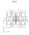
- Fig.1 is a schematic plan view of a micro-mirror device according to Embodiment 1 of the present invention.
- Fig. 2 is a cross sectional view of the micro-mirror device of Fig.1, shown along the line A-A.
- Fig.3 is a cross sectional view of another example the micro-mirror device according to Embodiment 1, shown along the same line A-A in Fig.1.
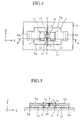
- Fig.4 is a schematic plan view of a micro-mirror device according to Embodiment 2 of the present invention.
- Fig. 5 is a cross sectional view of the micro-mirror device of Fig.4, shown along the line B-B.
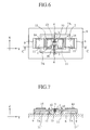
- Fig.6 is a schematic plan view of a micro-mirror device, using another driving force generating means, according to Embodiment 2 of the present invention.
- Fig. 7 is a cross sectional view of the micro-mirror device of Fig. 6, shown along the line C-C.
- Fig.8 is a schematic plan view of a micro-mirror device, according to Embodiment 2 of the present invention, using further another driving force generating means.
- Fig. 9 is a cross sectional view of the micro-mirror device of Fig. 8, shown along the line D-D.
- Fig.10 is a schematic plan view of a micro-mirror device, according to Embodiment 3 of the present invention.
- Fig.11 is a cross sectional view of the micro-mirror device of Fig. 10, shown along the line E-E.
- Fig. 12 is a schematic plan view of a micro-mirror device, according to Embodiment 4 of the present invention.
- Fig.13 is a cross sectional view of the micro-mirror device of Fig. 12, shown along the line F-F.
- Fig.14 is a schematic plan view of a micro-mirror device, according to Embodiment 4 of the present invention, using another driving force generating means, shown along the same line F-F in Fig.12.
- Fig.15 is a schematic plan view of a micro-mirror device, according to Embodiment 4 of the present invention, using another driving force generating means, shown along the same line F-F in Fig.12.
- Fig.16 shows processes for producing the micro-mirror device having the structure shown in Fig.15.
- Each of the figures is a cross sectional view of Fig.12 along the line F-F.
- Fig. 17 is a schematic plan view of the micro-mirror device in the prior art.
- Fig.18 is a cross sectional view of the micro-mirror device of Fig.17, shown along the line A-A.
- Fig.19 shows an example of voltages to be applied to the driving electrodes of the micro-mirror device.
- Embodiments of the micro-mirror device according to the present invention are explained below.
- Embodiment 1 is explained below, referring to Figs. 1 and 2.
- a mirror portion 1, made from thin metal layer, for example, aluminum layer, gold layer, etc, is formed on a mirror forming substrate 2.
- the mirror forming substrate 2 has a first torsion beam 3, which extends along a line in the direction X in Fig.19 perpendicular to a pair of opposing sides of the mirror forming substrate 2. Both the ends of the first torsion beam 3 are connected to a pair of first anchors 4.
- a supporting substrate 6 which is made from, for example, pyrex glass.
- a pair of first driving frames 7 are connected with the mirror forming substrate 2 through a first link beam 10.
- Each of the first driving frames 7 has a pair of second torsion beams 8. Both the ends of the second torsion beams 8 are supported by a pair of second anchors 9. Therefore, the first driving frames 7 are supported by the supporting substrate 6 through the second anchors 9.
- two first driving frames 7 are arranged, at both sides of the mirror forming substrate 2, in the direction Y in Fig.1.
- the pair of the second torsion beams 8 of each of the driving frame 7 extends along a line perpendicular to the opposing sides of the first driving frame 7.
- the first link beam 10 is disposed in each of the driving frames 7.
- the first link beam 10 of each of the first driving frames 7 is disposed in parallel with the first torsion beam 3 of the mirror forming substrate 2, and is connected with the mirror forming substrate 2 at a very near position to the base portion of the first torsion beam 3.
- a pair of sensor electrodes 11 are disposed on the supporting substrate 6 at positions under the mirror forming substrate 2.
- the sensor electrodes 11 monitor the light scanning angle ⁇ s of the mirror portion 1, by detecting the electrostatic capacity between the mirror forming substrate 2 and the sensor electrodes 11.
- a plurality of driving electrodes 12, as a driving force generating means, are disposed on the supporting substrate 6.
- the driving electrodes 12 generate an electrostatic attractive force depending on the voltage applied to them so as to drive the driving frame 7 to swing.
- two driving electrodes are disposed under each of the first driving frames 7, namely, four driving electrodes 12 are disposed in all.
- a stopper 13 is disposed for inhibiting an excessive displacement of the mirror forming substrate 2 in the Z direction shown in Fig.2.
- a direct voltage Vdc and alternating voltages Vac shown in Fig.19 are applied to the driving electrodes 12 disposed under the first driving frames 7 at the right and left sides of the mirror forming substrates 2.
- the alternating voltages applied to two driving electrodes 12 in each of the first driving frames 7 are in inverse phase, i.e. the phase difference between them is 180 degrees, both sides of the driving frames 7 displace oppositely in the direction Z shown in Fig. 2 so that the first driving frames swing around the second torsion beam 8, due to the electrostatic attractive forces between the driving electrodes 12 and the driving frames 7.
- the phase of the alternating voltages Vac to be applied to the driving electrode 12 corresponding to the first driving frame 7 disposed at the right side of the mirror forming substrate 2 is identical to that of the first driving frame 7 disposed at the left side of the mirror forming substrate 2, the right and left first driving frames 7 swing identically to each other.
- the driving force due to the torsional oscillation of the first driving frames 7 are transmitted indirectly to the mirror forming substrate 2 through the first link beam 10 so that the mirror forming substrate 2 swings, namely, a torsional oscillation of the mirror forming substrate 2 occurs.
- the first link beams 10 are connected to the mirror forming substrate 2 at a position very near to the base portion of the first torsion beam 3, and the connecting point between the second link beams 10 and the mirror forming substrate 3 is sufficiently far from the second torsion beam 8 of the first driving frames 7. Therefore, even when the displacements of the link beams 10 in the direction Z shown in Fig.2, are small, the magnitude of the swing of the mirror forming substrate 2 around the first torsion beam 3 can be amplified. In other words, giving a small torsion to the first driving frames 7, a large torsion of the mirror forming substrate 2 can be obtained. As a result, it is possible to obtain a micro-mirror device, in which a large maximum scanning angle ⁇ smax of the mirror portion 1 can be obtained, using a low driving voltage.
- Embodiment 1 Another example of Embodiment 1 is explained below, referring to Fig.3.
- a pair of grooves 15 are disposed on the supporting substrate 6 under the mirror forming substrate 2.
- the grooves function as recesses for avoiding the collision of the mirror forming substrate 2 to the supporting substrate 6.
- Components in Fig.3 identical to that in Fig.1 are referred by same reference numerals, and their explanations are omitted.
- the first driving frames 7 are driven by the electrostatic attractive forces between the first driving frames 7 and the driving electrodes 12. Therefore, the necessary driving voltage to be applied to the driving electrodes 7 can be decreased, by reducing the distance between the first driving frame 7 and the driving electrodes 12.
- the distance g2 of the gap between the first driving frame 7 and the driving electrodes 12 shown in Fig.3 is smaller than the distance g1 of the gap shown in Fig.2, i.e., g1 ⁇ g2.
- a groove 15 is disposed on the supporting substrate 6, therefore, the side ends of the mirror forming substrate 2 do not contact with the supporting substrate 6, when the mirror forming substrate 2 swing around the torsion beam 3.
- a sensor electrodes 11 for detecting the scanning angle ⁇ s are disposed on the supporting substrate 2 at a region under the mirror forming substrate 2 near to the base portion of the torsion beam 3, where the displacement in the direction Z is small.
- the motion of the mirror forming substrate 2 can be stabilized by these structure, namely the "pulled in phenomenon" does not occur, even when the distance between the first driving frames 7 and the driving electrodes 12 is designed to be small. Consequently, it is possible to reduce the necessary driving voltage.
- the micro-mirror device comprises: a supporting substrate 6; a mirror forming substrate 2, on which a mirror portion 1 is formed, a pair of first torsion beams 3 disposed on a pair of the opposing sides of the mirror forming substrate 2, which are perpendicular to those sides and support the mirror forming substrate 2; a first driving frame 7 surrounding at least one side of the mirror forming substrate 2 and connected to the mirror forming substrate 2 through a first link beam 10, which is disposed in parallel to the longitudinal direction of the first torsion beams 3; and a first driving force generating means 12 for driving the first driving frame 7 to move so that the movement is transmitted to the mirror forming substrate 2 through the first link beam 10.
- two first driving frames 7 are disposed at the right and left sides of the mirror forming substrate 2. However, it is possible to generate an oscillation of the mirror forming substrate 2, by disposing only one first driving frame 7 at one side of the mirror forming substrate 2.
- the first link beams 10 are connected with the mirror forming substrate 2 at a region near to the first torsion beam 3.
- the connecting points are not limited to this region. That is to say, even when the first link beams 10 can be connected to the mirror forming substrate 2 at a region not very near to the first torsion beam 3. Because a large swing of the mirror forming substrate 2 around its axis can be obtained by a small swing of the first driving frame 7 around the second torsion beam 8, when the size of the first driving frames 7 are made larger compared to that of the mirror forming substrate 2 so that the distance between the second torsion beam 8 and the connecting points between the first link beam 10 and the mirror forming substrate 2 is made larger.
- a driving force is transmitted from first driving frames to the mirror forming substrate through first link beams, in the same manner as in the embodiment 1.
- the first driving frames disposed at both sides of the mirror forming substrate are cantilevered, and the mirror forming substrate is driven to swing around its axis by the cantilever oscillation of the first driving frames.
- micro-mirror device according to the embodiment 2 is explained below, referring to Figs.4 and 5.
- a pair of first driving frames 7A are supported by a pair of anchor portions 9A (second driving frame side anchor portion), which are, in turn, supported by a supporting substrate 6.
- the anchor portions 9A are connected to a side of the first driving frames 7A.
- the first driving frames 7A have a cantilever structure supported by the anchor portions 9A and are fixed on the supporting substrate 6, as shown in Fig. 5.
- a pair of driving electrodes 12 (driving force generating means) for driving the first driving frames 7A are disposed on the supporting substrate 6 at the right and left side of the mirror forming substrate 2.
- the other components in the micro-mirror device according the embodiment 2 identical to that in Figs. 1 and 2 are referred by the same reference numerals, and their explanations are omitted.
- micro-mirror device according to the embodiment 2 is explained below.
- a biasing direct voltage Vdc is applied commonly between the first driving frames 7A and the driving electrodes 12 disposed on the supporting substrate 6 under the driving frames 7A.
- an alternating voltages Vac are superposed to the direct voltage.
- the phase of the alternating voltages Vac applied to the driving electrodes 12 corresponding to the first driving frames 7A disposed at right and left sides of the mirror forming substrate 2 are inverse to each other.
- An attracting electrostatic force is generated between the driving frames 7A and the driving electrodes 12.
- the first driving frames 7A swing around its base portion, in the direction Z in Fig.5, i.e. a cantilever oscillation of the driving frames 7A occurs.
- the driving force caused by the cantilever oscillation of the first driving frame 7A is transmitted indirectly to the mirror forming substrate 2 so that both sides of the mirror forming substrate 2 move in the direction Z perpendicular to the supporting substrate 6.
- the mirror forming substrate 2 swings around the first torsion beam 3, namely a torsional oscillation of the mirror forming substrate 2 occurs.
- a micro-mirror device operable which can scan the light beam in a wide maximum scanning angle ⁇ smax, using a low driving voltage, can be obtained.
- a pair of sensor electrodes 11' are disposed on the supporting substrate 6 at a region just under the first driving frame 7.
- the sensor electrodes monitor the scanning angle of the mirror forming substrate 2, on the basis of the displacement of the first driving frame 7A.
- the electrostatic capacity between mirror forming substrate 2 and the sensor electrodes 11 disposed just under the mirror forming substrate 2 is proportional to the inverse of the distance between the mirror forming substrate 2 and the sensor electrodes 11'.
- This relation does not stand, when the scanning angle of the mirror forming substrate in the torsional movement of the mirror forming substrate 2 becomes large.
- the sensor electrodes are disposed at a region just under the first driving frames 7A, for avoiding this problem.
- a piezoelectric element 14 as a driving force generating means are disposed on the first driving frame 7A.
- the piezoelectric elements 14 are made from, for example, conventional bulk piezoelectric element or thin layer piezoelectric element. Components in Figs. 6 and 7 identical to that in Figs. 4, and 5 are referred by the same reference numerals, and their explanations are omitted.
- the driving force due to the cantilever oscillation of the first driving frame 7A are transmitted indirectly to the mirror forming substrate 2 through the first link beam 10.
- a torsional oscillation of the mirror forming substrate 2 around the torsion beam 3 occurs, when two sides of the mirror forming substrate 2 move oppositely in the direction Z in Fig.7.
- a pair of sensor electrodes 11' are disposed on the supporting substrate 6 at a region just under the first driving frame 7.
- the sensor electrodes monitor the scanning angle of the mirror forming substrate 2, on the basis of the displacement of the first driving frame 7A.
- the electrostatic capacity between mirror forming substrate 2 and the sensor electrodes 11 disposed just under the mirror forming substrate 2 is proportional to the inverse of the distance between the mirror forming substrate 2 and the sensor electrodes 11'.
- the sensor electrodes are disposed at a region just under the first driving frames 7A, for eliminating this influence.
- Permanent magnets 14A are disposed on the first driving frame 7A as a driving force generating means.
- the permanent magnets 14A are made from conventional bulk magnetic element or thin layer magnetic element. In the example shown in the figure, the magnetic polarities of the magnets 14A are configured oppositely in the direction Z in Fig. 9.
- a solenoid coil 21 supported by a coil supporting core 22 is disposed so as to surround the micro-mirror device.
- the solenoid coil 21 and the coil supporting core 22 form an electromagnet 14B as a driving force generating means.
- Components in Figs. 8 and 9 identical to that in Figs. 4 and 6 are referred by the same reference numerals, and their explanations are omitted.
- the mirror forming substrates 2 swings in the direction Z in Fig.9, namely, a torsional oscillation of the mirror forming substrate 2 around the first torsion beam 3 appears.
- Other functions of this example are identical to the other examples of the micro-mirror device according to the embodiment 2. Thus, their explanations are omitted.
- the permanent magnets 14A are disposed on the driving frame side, and the electromagnet 14B is disposed to surround the micro-mirror device, for driving the first driving frames 7A.
- the electromagnet 14B is disposed to surround the micro-mirror device, for driving the first driving frames 7A.
- a driving system using electrostatic force generated by driving electrodes 12 or a driving system using magnetic force generated by a pair of magnets comprised of an permanent magnet and an electromagnet is used.
- driving system using electrostatic force generated by driving electrodes 12 or a driving system using magnetic force generated by a pair of magnets comprised of an permanent magnet and an electromagnet is used.
- the scanning angle of the mirror forming substrate can be sensed using a piezoelectric element (not shown) disposed on the first driving frame at a position near to the base portion of the first driving frame 7A, which detects the change of the electric resistivity caused by the deformation of the first driving frame 7A.
- the first driving frame 7A is supported by an anchor portion (9A) projecting from the supporting substrate (6), and the first driving frame 7A comprises a driving force generating means, for example, driving electrodes 12, piezoelectric element 14, or a coupling of an permanent magnet and an electromagemet.
- a driving force generating means for example, driving electrodes 12, piezoelectric element 14, or a coupling of an permanent magnet and an electromagemet.
- a groove 15 can be disposed on the supporting substrate 6 at a region under the mirror forming substrate 2, for avoiding the collision of a mirror forming substrate to the supporting substrate 6. Disposing the groove, the distance of the gap between the first driving frame 7A and driving electrodes 12 can be decreased. And as a result, the driving voltage can be lowered.
- the light beam is scanned in one dimension.
- the light beam is scanned two dimensionally.
- micro-mirror device according to the embodiment 3 is explained below, referring to Figs. 10 and 11.
- a first driving frame 7B is connected with a mirror forming substrate 2 through a first link beam 10.
- a second driving frame 7C is connected with the first driving frame 7B through a third link beam 18.
- the first driving frame 7B has a pair of third torsion beam 16, parallel to the direction Y in Fig. 10, at the center of two sides of the first driving frame 7B.
- the third torsion beams 16 are perpendicular to the direction of the first link beams 10.
- the first driving frame 7B is supported by the pair of the third torsion beams 16, and the third torsion beams, in turn, are fixed to the supporting substrate 6 through a pair of third anchor portions 9B.
- Each of the third anchor portion 9B and the third torsion beam 16 form a cantilever structure.
- the second driving frames 7C are fixed to the supporting substrate 6 through a pair of fourth anchor portions 9C.
- Each of the fourth anchor portions 9C and the second driving frame 7C form a cantilever structure in the same manner as the first driving frames.
- Two pairs of piezoelectric elements 14 as driving force generating means are disposed on each of the driving frames 7B, 7C.
- a pair of third torsion beams 16 (second driving frame side torsion beam) are disposed, in parallel to the direction Y in Fig.10, at the center of opposing sides of the first driving frame 7B.
- two pairs of second link beam 18 (inter driving frame link beam) are disposed at a region very near to the third torsion beam 16.
- a pair of sensor electrodes 19 are disposed on the supporting substrate 6 at a region under the first driving frame 7B.
- the scanning angles ⁇ s of the light beam around the two scanning axis (torsion beam 3,16) are detected, using the sensor electrodes 19 and the sensor electrodes 11 disposed on the supporting substrate 6 at a region under the mirror forming substrate 2.
- Components in Fig.10 identical to that in Figs.1 to 9 are referred by the same reference numeral, and their explanations are omitted.
- micro-mirror device according to the embodiment 3 is explained below.
- the scanning angles around two axes can be monitored as follows.
- the scanning angle ⁇ s around the first torsion beam 3 is monitored by the sensor electrodes 11 disposed on the supporting substrate 6 at a region under the mirror forming substrate 2.
- the sensor electrodes 11 detect the electrostatic capacity between the mirror forming substrate 2 and the sensor electrodes 11.
- the scanning angle ⁇ s around the third torsion beams 16 is monitored by the sensor electrodes 19 disposed on the supporting substrate 6 at a region under the second driving frames 7C.
- the sensor electrodes 19 detect the electrostatic capacity between the second driving frames 7C and the sensor electrodes.
- the scanning angles can be monitored, using piezoresistors disposed near to their anchor portions.
- the electric resistivity of a piezoresistor changes according to its deformation, for example, due to the oscillation of the driving frames. Therefore, the scanning angle of the mirror forming substrate 2 can be monitored by detecting the displacement of the driving frames, on the basis of the change of the electric resistivity.
- the first and second driving frames 7B, 7C are driven by piezoelectric elements 14, however, the driving force generating means are not limited to piezoelectric elements 14.
- the driving force can be obtained from, for example, an attractive electrostatic force between a pair of driving electrodes, an attractive force between a pair of magnets, or a combination of them, which have been explained in detail.
- the micro-mirror device further comprises: a second driving frame 7C; the ends of the first torsion beams 3 are supported by the first driving frame 7B; the first driving frame 7B has third torsion beams 16, disposed on one side of the first driving frame 7B opposing to the first link beam 10, perpendicular to the first torsion beam 3; the ends of the third torsion beams 16 are supported by a pair of third anchor portions 9B projecting from the supporting substrate 6; the second driving frame 7C is connected to the first driving frame 7B through a second link beam 18, which is disposed at one side of the second driving frame 7C in parallel to the longitudinal direction of the third torsion beams 16.
- each of the first and second driving frames 7B, 7C comprise a driving force generating means, for example, driving electrodes 12, piezoelectric element 14, or a coupling of an permanent magnet and an electromagnet.
- a large displacement of the mirror forming substrate 2 in the directions XY in Fig.2 can be obtained, corresponding to the small displacement of the first and second driving frame 7B, 7C.
- the maximum scanning angles ⁇ smax around two axes is large. And, two dimensional scanning of a light beam using a mirror forming substrate is possible, using a low driving voltage.
- a pair of grooves 15 can be disposed on the supporting substrate 6 at a region under the mirror forming substrate 2 for avoiding the collision of the mirror forming substrate 2 to the supporting substrate 6, when a pair of driving electrodes are used as a driving force generating means, in the same manner as in the embodiment 1.
- the distance between the supporting substrate 6 and each of the driving frames 7B, 7C can be decreased, and the necessary driving voltage can be lowered.
- two first driving frames 7B are disposed at both right and left portions of the mirror forming substrate 2
- two second driving frames 7C are disposed at both right and left sides of the first driving frames 7B, however, it is possible to dispose only one first driving frame 7B at one side of the mirror forming substrate 2 or only one second driving frame 7C at one side of the first driving frame 7B so that a cantilever oscillation occurs on each of them.
- the first link beams 10 are disposed very near to the torsion beam 3, and the second link beams 18 are disposed very near to the torsion beam 16, however the connecting positions between the mirror forming substrate and the driving frames 7B and between the driving frames 7B and the driving frames 7C are not limited to such positions.
- the link beams 10, 18 can be positioned at a region a little far from the link beams 3, 16.
- micro-mirror device according to the embodiment 4 of the present invention is explained below, referring to Figs. 12, 13.
- a mirror 1 is formed on a mirror forming substrate 2A, which is connected with a first driving frame 7D through a first torsion beam 3.
- the mirror forming substrate 2A is not symmetrical with respect to the first torsion bean 3.
- the mirror forming substrate 2A has a planer structure, in which the driving frame side half area (left portion) of the mirror forming substrate 2 is larger compared to the rest half (right portion).
- the first driving frame 7D can be driven, for example, by an electrostatic force caused by driving electrodes 12, or by an oscillation of piezoelectric elements 14.
- the driving electrodes 12 and the piezoelectric elements 14 are commonly shown in Figs.12, 13.
- the other components in Figs.12. 13 identical to that in Fig.1 to 9 are referred by the same reference numerals, and their explanations are omitted.
- the first driving frame 7D are driven by driving electrodes 12.
- a direct voltage Vdc and an alternating voltages Vac which are explained in the embodiment 1, are applied between the first driving frame 7D and the driving electrode 12 disposed on the supporting substrate 6 at a region under the first driving frames 7D.
- a cantilever oscillation of the first driving frame 7D around an anchor portion 9A occurs in the direction Z.
- the driving force of the first driving frame 7D is transmitted to the mirror forming frame 2 through the first torsion beam 3.
- the transmitted force acts as an inertia force to the mirror forming substrate 2.
- the mirror forming substrate has a planer structure, which is not symmetrical with respect to the torsion beam 3, and its center of the weight is not on the torsion beam 3, a torsional torque around the torsion beam 3 is generated by the inertia force from the first driving frame 7D. As a result, an oscillation of the mirror forming substrate 2 around the torsion beam 3 occurs.
- Piezoelectric elements as a driving force generating means are shown in Figs.12, 13, however, their explanation is omitted, because they are explained in the other embodiments.
- the driving force generating means are not limited to such an amendment.
- a pair of magnets, which has been explained in the embodiment 2, or combinations of these driving force generating means can be employed as a driving force generating means.
- micro-mirror device Another example of the micro-mirror device according to the embodiment 4 is explained below, referring to Fig. 14.
- a groove 15 is disposed on the supporting substrate-6 at a region under the mirror forming substrate 2A for preventing the collision of the mirror forming substrate 2 to the supporting substrate 6.
- the distance between the first driving frame 7D and the driving electrodes 12 can be decreased. Therefore, the necessary driving voltage for driving the first driving frame 7D, by an attracting electrostatic force between a pair of driving electrodes as a driving force generating means, can be lowered.
- the mirror forming substrate 2B is thin so that the distance between the mirror forming substrate 2B and the supporting substrate 6 can be sufficiently large.
- the mirror forming substrate 2B is aligned with the upper surface of the first driving frame 7D so that the distance between the mirror forming substrate 2B and the supporting substrate 6 can be as large as possible.
- this structure it is not necessary to make a groove 15 such as shown in Fig.14, therefore the structure of the micro-mirror device can be simplified, and simultaneously the distance between the first driving frame 7D and the driving electrodes 12 can be decreased. Therefore, the necessary driving voltage for driving the driving frame 7D, by an attracting electrostatic force between a pair of driving electrodes 12 and the driving frames, can be lowered.
- the scanning angle of the mirror can be monitored by a piezoresistor disposed on the first driving frame 7D at a region near to the anchor portion, on the basis of the change of electric resistivity of a piezoresitor caused by the displacement of the first driving frame 7D.
- the micro-mirror device comprises: a mirror forming substrate 2A, 2B, on which a mirror portion 1 is formed; a first torsion beam 3 disposed on a pair of opposing sides of the mirror forming substrate 2A, 2B; a first driving frame 7D, disposed at the outer portion of the mirror forming substrate 2A, 2B and supporting the first torsion beam 3; and a driving force generating means for giving a driving force to the first driving frame 2A, 2B.
- the driving force generating means comprises, for example, driving electrode 12, piezoelectric element 14, and a pair of magnets composed of an permanent magnet and an electromagnet.
- the micro-mirror device according to the embodiment 4 has a simple structure compared to that of the embodiments 1 and 2, however, it has similar advantages as that of the embodiments 1 and 2.
- the embodiment 5 of the present invention relates to a method for producing a micro-mirror device according to the present invention.
- the method for producing a micro-mirror device having the structure shown in Fig.15 is explained here, as an example of the method for producing a micro-mirror devices according to the embodiments 1 to 4. However, the method is basically applicable to the micro-mirror devices according to the other embodiments.
- Etching patterns for forming a mirror forming substrate 2B and a first torsion beam 3 are formed on a first layer etching mask 23, which is made from a resist layer in this example.
- An etching pattern for forming a driving frame 7D is formed on a second etching mask 24.
- the second etching mask 24 is made from a thin metal layer such as a thin aluminum layer which can resist when the resist layer as an etching mask 23 of the first etching layer 23 is removed.
- a pattern for forming a pair of anchor portions 9A of the driving frame 7D is formed on a third etching mask 25.
- the third etching mask 25 is made from an oxidized layer which can resist when the thin metal layer as an etching mask 24 of the second etching layer 24 is removed.
- the structured body of a micro-mirror device is formed from a device wafer 26.
- a silicon single crystal substrate having (100) surface is used, because it is cheaply available as a material substrate.
- Reference numeral 27 denotes a handle wafer, which will be removed when the production process is completed.
- the device wafer 26 and the handle wafer 27 are jointed through a oxidized layer 25' to constitute a material substrate 28, so-called SOI (Silicon On Insulator) substrate.
- SOI Silicon On Insulator
- a micro-mirror device is fabricated as follows: At first, the first, second and third etching masks 23, 24, 25 are formed in sequence on the SOI substrate at its device wafer side 26, applying conventional etching mask forming processes and patterning processes, for example, photo-lithography process, sputtering process, etching process, etc.
- the material of an inner layer etching mask shall be selected from a material that can resist when the outer layer, which is near to the outer surface, is removed.
- the structure of the multi-layer etching mask shall be designed so that a structured body, which contains vertical portions extending in the direction Z, such as the pair of anchor portions 9A in Fig.16, is formed, by not being removed by the etching processes.
- a highly anisotropic etching of the SOI substrate 28 is performed from the outer side etching mask 23.
- the SOI substrate 28 is etched in the direction perpendicular to the surface (direction Z in Fig.16).
- Such a highly anisotropic etching can be carried out using a commercially available silicon dry etching apparatus (for example, ICP-RIE apparatus).
- ICP-RIE apparatus for example, ICP-RIE apparatus
- Fig.16(a) is a cross sectional view of a SOI substrate after highly anisotropic etching of the outer side etching mask 23.
- the resist layer as a first etching mask 23 is removed, applying so-called O 2 ashing process.
- the thin metal layer as a second etching mask 24 appears on the surface.
- Another highly anisotropic etching is carried out to this second etching mask 24 in the same manner as in the etching of the first etching mask 23.
- the second etching is completed, the structure formed by the first etching is maintained, and a structure with a homogeneous etching depth in the vertical direction (the direction Z in Fig.16) is obtained.
- the third etching mask 25 made from oxidized layer appears on the surface.
- the surface portion of the SOI subtrate 28 is removed over about 5 micro-meter depth from the original surface.
- the structured body shown in Fig.16 (c) is formed.
- the SOI substrate, on which the structured body is formed is treated by hydrofluoric acid to remove the etching mask 25.
- the anchor portions 28 of the SOI substrate 28, on which the structured body is formed is connected with a supporting substrate 6 made from, for example, pyrex glass, on which metal electrodes (driving electrodes 12 and sensor electrodes 11) are disposed, so that a structure shown in Fig.16 (d) is obtained.
- the handle wafer 27 of this structured body is removed by wet etching process or by dry etching process, as shown in Fig.16 (e).
- the rest oxidized layer 25' can be removed by hydrofluoric acid treatment.
- thin metal layers such as aluminum or chromium/gold layer, are formed on the mirror forming substrate 2B and on the driving frame 7D, for making for example, a mirror portion 1, applying a so-called selective sputtering method or selective evaporation method.
- a micro-mirror device is accomplished, by forming a pair of piezoelectric elements 14, as driving means, on the first driving frames 7D (Fig.16 (f)).
- etching masks 23, 24, 25, on which patterns corresponding to the components of a micro-mirror device are formed are formed on an SOI substrate 28 to form a multi-layer; then an anisotropic etching process and an etching mask removing process are carried out alternatively to the SOI substrate 28 from the outer etching mask 23 so as to form the components of a micro-mirror device to obtain a micro-mirror device.
- the etching masks can be previously formed on a flat smooth plane, therefore, a precise patterning of a etching mask is possible.
- etching on the SOI substrate is performed only from the upper side surface of the SOI substrate.
- the substrate is not limited to an SOI substrate.
- Etching masks can be multi-layer etching masks disposed on both sides of a material substrate so that the etching process can be performed from both sides of the material substrate. In this case, the patterning of the etching masks can be carried out from both sides of the material substrate, and a precise alignment is possible.
Landscapes
- Physics & Mathematics (AREA)
- General Physics & Mathematics (AREA)
- Optics & Photonics (AREA)
- Engineering & Computer Science (AREA)
- Computer Hardware Design (AREA)
- Microelectronics & Electronic Packaging (AREA)
- Micromachines (AREA)
- Mechanical Optical Scanning Systems (AREA)
- Mechanical Light Control Or Optical Switches (AREA)
Applications Claiming Priority (2)
| Application Number | Priority Date | Filing Date | Title |
|---|---|---|---|
| JP15059099 | 1999-05-28 | ||
| JP11150590A JP3065611B1 (ja) | 1999-05-28 | 1999-05-28 | マイクロミラ―装置およびその製造方法 |
Publications (3)
| Publication Number | Publication Date |
|---|---|
| EP1058143A2 true EP1058143A2 (fr) | 2000-12-06 |
| EP1058143A3 EP1058143A3 (fr) | 2003-08-06 |
| EP1058143B1 EP1058143B1 (fr) | 2005-01-19 |
Family
ID=15500221
Family Applications (1)
| Application Number | Title | Priority Date | Filing Date |
|---|---|---|---|
| EP99119183A Expired - Lifetime EP1058143B1 (fr) | 1999-05-28 | 1999-10-07 | Dispositif à micromirroir et méthode de fabrication de ce dispositif |
Country Status (4)
| Country | Link |
|---|---|
| US (1) | US6259548B1 (fr) |
| EP (1) | EP1058143B1 (fr) |
| JP (1) | JP3065611B1 (fr) |
| DE (1) | DE69923294T2 (fr) |
Cited By (6)
| Publication number | Priority date | Publication date | Assignee | Title |
|---|---|---|---|---|
| WO2002054475A1 (fr) | 2001-01-02 | 2002-07-11 | The Charles Stark Draper Laboratory, Inc. | Procede de microusinage de structures utilisant un materiau de silicium sur isolant |
| WO2004033365A3 (fr) * | 2002-10-07 | 2004-08-26 | Freescale Semiconductor Inc | Procede de formation d'un capteur de detection de mouvement |
| US6917399B2 (en) | 2001-02-22 | 2005-07-12 | 3M Innovative Properties Company | Optical bodies containing cholesteric liquid crystal material and methods of manufacture |
| DE102007052804B4 (de) * | 2006-11-09 | 2012-12-06 | Mitsubishi Electric Corp. | Beschleunigungssensor |
| US8809135B2 (en) | 2001-01-02 | 2014-08-19 | The Charles Stark Draper Laboratory, Inc. | MEMS device and interposer and method for integrating MEMS device and interposer |
| US12259546B2 (en) | 2019-08-19 | 2025-03-25 | Asml Netherlands B.V. | Micromirror arrays |
Families Citing this family (45)
| Publication number | Priority date | Publication date | Assignee | Title |
|---|---|---|---|---|
| DE19857946C1 (de) * | 1998-12-16 | 2000-01-20 | Bosch Gmbh Robert | Mikroschwingspiegel |
| US7064879B1 (en) * | 2000-04-07 | 2006-06-20 | Microsoft Corporation | Magnetically actuated microelectrochemical systems actuator |
| US6639711B2 (en) * | 2000-09-20 | 2003-10-28 | Texas Instruments Incorporated | Packaged micromirror assembly with in-package mirror position passive component feedback |
| US6775048B1 (en) * | 2000-10-31 | 2004-08-10 | Microsoft Corporation | Microelectrical mechanical structure (MEMS) optical modulator and optical display system |
| US6803843B2 (en) * | 2001-02-22 | 2004-10-12 | Canon Kabushiki Kaisha | Movable-body apparatus, optical deflector, and method of fabricating the same |
| JP2002258174A (ja) * | 2001-03-02 | 2002-09-11 | Seiko Epson Corp | 光変調装置及びそれを有する電子機器 |
| JP2002307396A (ja) * | 2001-04-13 | 2002-10-23 | Olympus Optical Co Ltd | アクチュエータ |
| KR100400742B1 (ko) * | 2001-04-19 | 2003-10-08 | 엘지전자 주식회사 | 압전 구동형 미소 거울 및 그 제조방법 |
| US6695457B2 (en) * | 2001-06-02 | 2004-02-24 | Capella Photonics, Inc. | Bulk silicon mirrors with hinges underneath |
| JP2003005101A (ja) * | 2001-06-26 | 2003-01-08 | Seiko Epson Corp | 光変調装置及びその製造方法 |
| US6701037B2 (en) * | 2001-07-03 | 2004-03-02 | Pts Corporation | MEMS-based noncontacting free-space optical switch |
| US6844952B2 (en) * | 2001-09-18 | 2005-01-18 | Vitesse Semiconductor Corporation | Actuator-controlled mirror with Z-stop mechanism |
| KR100443368B1 (ko) * | 2001-10-09 | 2004-08-09 | 한국과학기술원 | 미소 평판 구동 장치 |
| JP2006502421A (ja) * | 2001-11-06 | 2006-01-19 | キーオティ | 画像投影装置 |
| US6804959B2 (en) * | 2001-12-31 | 2004-10-19 | Microsoft Corporation | Unilateral thermal buckle-beam actuator |
| US7053519B2 (en) * | 2002-03-29 | 2006-05-30 | Microsoft Corporation | Electrostatic bimorph actuator |
| JP4140816B2 (ja) * | 2002-05-24 | 2008-08-27 | 富士通株式会社 | マイクロミラー素子 |
| KR100431581B1 (ko) * | 2002-05-28 | 2004-05-17 | 한국과학기술원 | 미소거울 구동기 |
| US7019876B2 (en) * | 2002-07-29 | 2006-03-28 | Hewlett-Packard Development Company, L.P. | Micro-mirror with rotor structure |
| US7208809B2 (en) | 2002-09-19 | 2007-04-24 | Nippon Telegraph And Telephone Corporation | Semiconductor device having MEMS |
| JP3833988B2 (ja) * | 2002-11-01 | 2006-10-18 | 日本電信電話株式会社 | 光スイッチ装置 |
| US7993285B2 (en) * | 2002-11-05 | 2011-08-09 | Boston Scientific Scimed, Inc. | Medical device having flexible distal tip |
| US6835589B2 (en) * | 2002-11-14 | 2004-12-28 | International Business Machines Corporation | Three-dimensional integrated CMOS-MEMS device and process for making the same |
| US7050271B2 (en) * | 2002-11-28 | 2006-05-23 | Tdk Corporation | Actuator having doped silicon arms and method of making the same |
| US7182262B2 (en) * | 2003-03-13 | 2007-02-27 | Symbol Technologies, Inc. | Inertial drive scanning arrangement and method |
| US7095546B2 (en) * | 2003-04-24 | 2006-08-22 | Metconnex Canada Inc. | Micro-electro-mechanical-system two dimensional mirror with articulated suspension structures for high fill factor arrays |
| US6992422B2 (en) * | 2003-06-11 | 2006-01-31 | Texas Instruments Incorporated | Position sensor for a pivoting platform |
| JP4695342B2 (ja) * | 2003-09-03 | 2011-06-08 | 富士通株式会社 | 光スイッチ制御装置および移動体制御装置 |
| JP2005128147A (ja) * | 2003-10-22 | 2005-05-19 | Stanley Electric Co Ltd | 光偏向器及び光学装置 |
| US7485485B2 (en) * | 2004-02-09 | 2009-02-03 | Microvision, Inc. | Method and apparatus for making a MEMS scanner |
| JP4499447B2 (ja) * | 2004-03-01 | 2010-07-07 | 日本電信電話株式会社 | 電子部品装置 |
| JP4287324B2 (ja) * | 2004-04-28 | 2009-07-01 | 日本電信電話株式会社 | 電子部品装置 |
| US7442918B2 (en) * | 2004-05-14 | 2008-10-28 | Microvision, Inc. | MEMS device having simplified drive |
| US7636101B2 (en) | 2005-02-09 | 2009-12-22 | Microvision, Inc. | MEMS scanner adapted to a laser printer |
| US7432629B2 (en) * | 2005-02-16 | 2008-10-07 | Jds Uniphase Corporation | Articulated MEMs structures |
| RU2277255C1 (ru) * | 2005-03-28 | 2006-05-27 | Государственное образовательное учреждение высшего профессионального образования "Таганрогский государственный радиотехнический университет" (ТРТУ) | Интегральное микромеханическое зеркало |
| US7978388B2 (en) * | 2006-01-12 | 2011-07-12 | Nippon Telegraph And Telephone Corporation | Mirror device and mirror device manufacturing method incorporating a collision preventive structure |
| US7779522B2 (en) * | 2006-05-05 | 2010-08-24 | Fujifilm Dimatix, Inc. | Method for forming a MEMS |
| JP5023952B2 (ja) * | 2007-10-11 | 2012-09-12 | セイコーエプソン株式会社 | アクチュエータ、光スキャナおよび画像形成装置 |
| JP5172364B2 (ja) * | 2008-01-16 | 2013-03-27 | スタンレー電気株式会社 | 光偏向器 |
| EP2708308A1 (fr) * | 2012-09-14 | 2014-03-19 | Trumpf Laser Marking Systems AG | Dispositif de traitement laser |
| DE102014211546B4 (de) | 2014-06-17 | 2022-08-25 | Robert Bosch Gmbh | Mikrospiegelanordnung |
| DE102014215048A1 (de) | 2014-07-31 | 2016-02-04 | Robert Bosch Gmbh | Mikrospiegelvorrichtung, Mikrospiegelarray und Projektionseinrichtung |
| JP6840069B2 (ja) * | 2017-12-14 | 2021-03-10 | 三菱電機株式会社 | 微小電子機械デバイスの検査方法 |
| JP6973198B2 (ja) * | 2018-03-12 | 2021-11-24 | オムロン株式会社 | 光偏向器、及びライダー装置 |
Family Cites Families (5)
| Publication number | Priority date | Publication date | Assignee | Title |
|---|---|---|---|---|
| JP3003429B2 (ja) * | 1992-10-08 | 2000-01-31 | 富士電機株式会社 | ねじり振動子および光偏向子 |
| US5710657A (en) * | 1994-02-23 | 1998-01-20 | Aura Systems, Inc. | Monomorph thin film actuated mirror array |
| US5629794A (en) * | 1995-05-31 | 1997-05-13 | Texas Instruments Incorporated | Spatial light modulator having an analog beam for steering light |
| WO1996039643A1 (fr) * | 1995-06-05 | 1996-12-12 | Nihon Shingo Kabushiki Kaisha | Actionneur electromagnetique |
| EP1012890A1 (fr) * | 1997-04-01 | 2000-06-28 | Xros, Inc. | Ajustement des caracteristiques de fonctionnement d'oscillateurs a torsion micro-usines |
-
1999
- 1999-05-28 JP JP11150590A patent/JP3065611B1/ja not_active Expired - Fee Related
- 1999-09-23 US US09/401,947 patent/US6259548B1/en not_active Expired - Fee Related
- 1999-10-07 DE DE69923294T patent/DE69923294T2/de not_active Expired - Fee Related
- 1999-10-07 EP EP99119183A patent/EP1058143B1/fr not_active Expired - Lifetime
Cited By (8)
| Publication number | Priority date | Publication date | Assignee | Title |
|---|---|---|---|---|
| WO2002054475A1 (fr) | 2001-01-02 | 2002-07-11 | The Charles Stark Draper Laboratory, Inc. | Procede de microusinage de structures utilisant un materiau de silicium sur isolant |
| EP1364398A4 (fr) * | 2001-01-02 | 2011-11-30 | Draper Lab Charles S | Procede de microusinage de structures utilisant un materiau de silicium sur isolant |
| US8809135B2 (en) | 2001-01-02 | 2014-08-19 | The Charles Stark Draper Laboratory, Inc. | MEMS device and interposer and method for integrating MEMS device and interposer |
| US6917399B2 (en) | 2001-02-22 | 2005-07-12 | 3M Innovative Properties Company | Optical bodies containing cholesteric liquid crystal material and methods of manufacture |
| US7277141B2 (en) | 2001-02-22 | 2007-10-02 | 3M Innovative Properties Company | Optical bodies containing cholesteric liquid crystal material and methods of manufacture |
| WO2004033365A3 (fr) * | 2002-10-07 | 2004-08-26 | Freescale Semiconductor Inc | Procede de formation d'un capteur de detection de mouvement |
| DE102007052804B4 (de) * | 2006-11-09 | 2012-12-06 | Mitsubishi Electric Corp. | Beschleunigungssensor |
| US12259546B2 (en) | 2019-08-19 | 2025-03-25 | Asml Netherlands B.V. | Micromirror arrays |
Also Published As
| Publication number | Publication date |
|---|---|
| EP1058143A3 (fr) | 2003-08-06 |
| US6259548B1 (en) | 2001-07-10 |
| JP2000338445A (ja) | 2000-12-08 |
| JP3065611B1 (ja) | 2000-07-17 |
| EP1058143B1 (fr) | 2005-01-19 |
| DE69923294T2 (de) | 2005-12-29 |
| DE69923294D1 (de) | 2005-02-24 |
Similar Documents
| Publication | Publication Date | Title |
|---|---|---|
| EP1058143B1 (fr) | Dispositif à micromirroir et méthode de fabrication de ce dispositif | |
| US5914801A (en) | Microelectromechanical devices including rotating plates and related methods | |
| US6044705A (en) | Micromachined members coupled for relative rotation by torsion bars | |
| US5959760A (en) | Light beam scanner using large electrostatic force | |
| US4317611A (en) | Optical ray deflection apparatus | |
| US6595055B1 (en) | Micromechanical component comprising an oscillating body | |
| US6538799B2 (en) | Magnetically actuated torsional micro-mechanical mirror system | |
| KR100816049B1 (ko) | 컴바인드 센서와 그 제조방법 | |
| USRE42359E1 (en) | Dynamical quantity sensor | |
| US5648618A (en) | Micromachined hinge having an integral torsion sensor | |
| US6831765B2 (en) | Tiltable-body apparatus, and method of fabricating the same | |
| TWI432777B (zh) | 具有降低之動態變形的微機電系統掃描微鏡 | |
| JP4385937B2 (ja) | アクチュエータ | |
| US7808150B2 (en) | Actuator having deflected fixed comb electrodes and movable comb electrodes | |
| EP1225469B1 (fr) | Dispositif de balayage à laser micro-opto-électromécanique intégré | |
| US7453182B2 (en) | Micro oscillating element | |
| JP2006171349A (ja) | アクチュエータ | |
| CN100410724C (zh) | 梳齿电极对的制造方法 | |
| US20210011282A1 (en) | Optical scanning device and method of control therefor | |
| JP2002321196A (ja) | マイクロ構造体、マイクロ力学量センサ、マイクロアクチュエータ、マイクロ光偏向器、光走査型ディスプレイ、及びそれらの製造方法 | |
| JP4544823B2 (ja) | 熱memsアクチュエータの面外作動方法及び熱memsアクチュエータ | |
| WO2009044324A2 (fr) | Procédé de fabrication de micro-miroir à balayage mems | |
| JP2006167860A (ja) | アクチュエータ | |
| JP2006201520A (ja) | Memsミラースキャナ | |
| JP2003098444A (ja) | ミラー偏向装置及び光交換装置 |
Legal Events
| Date | Code | Title | Description |
|---|---|---|---|
| PUAI | Public reference made under article 153(3) epc to a published international application that has entered the european phase |
Free format text: ORIGINAL CODE: 0009012 |
|
| AK | Designated contracting states |
Kind code of ref document: A2 Designated state(s): AT BE CH CY DE DK ES FI FR GB GR IE IT LI LU MC NL PT SE |
|
| AX | Request for extension of the european patent |
Free format text: AL;LT;LV;MK;RO;SI |
|
| PUAL | Search report despatched |
Free format text: ORIGINAL CODE: 0009013 |
|
| AK | Designated contracting states |
Designated state(s): AT BE CH CY DE DK ES FI FR GB GR IE IT LI LU MC NL PT SE |
|
| AX | Request for extension of the european patent |
Extension state: AL LT LV MK RO SI |
|
| 17P | Request for examination filed |
Effective date: 20031001 |
|
| 17Q | First examination report despatched |
Effective date: 20031117 |
|
| AKX | Designation fees paid |
Designated state(s): DE FR GB |
|
| GRAP | Despatch of communication of intention to grant a patent |
Free format text: ORIGINAL CODE: EPIDOSNIGR1 |
|
| GRAS | Grant fee paid |
Free format text: ORIGINAL CODE: EPIDOSNIGR3 |
|
| GRAA | (expected) grant |
Free format text: ORIGINAL CODE: 0009210 |
|
| RIN1 | Information on inventor provided before grant (corrected) |
Inventor name: MITA, YOSHIO Inventor name: TOSHIYOSHI, HIROSHI Inventor name: MITA, MAKOTO Inventor name: FUJITA, HIROYUKI Inventor name: KONNO, NOBUAKI Inventor name: TSUGAI, MASAHIRO |
|
| AK | Designated contracting states |
Kind code of ref document: B1 Designated state(s): DE FR GB |
|
| REG | Reference to a national code |
Ref country code: GB Ref legal event code: FG4D |
|
| REG | Reference to a national code |
Ref country code: IE Ref legal event code: FG4D |
|
| REF | Corresponds to: |
Ref document number: 69923294 Country of ref document: DE Date of ref document: 20050224 Kind code of ref document: P |
|
| RIN2 | Information on inventor provided after grant (corrected) |
Inventor name: MITA, YOSHIO Inventor name: HIROSHI,TOSHIYOSHI Inventor name: MITA, MAKOTO Inventor name: FUJITA, HIROYUKI Inventor name: KONNO, NOBUAKI Inventor name: TSUGAI, MASAHIRO |
|
| REG | Reference to a national code |
Ref country code: GB Ref legal event code: 727 |
|
| REG | Reference to a national code |
Ref country code: GB Ref legal event code: 727A |
|
| ET | Fr: translation filed | ||
| PLBE | No opposition filed within time limit |
Free format text: ORIGINAL CODE: 0009261 |
|
| STAA | Information on the status of an ep patent application or granted ep patent |
Free format text: STATUS: NO OPPOSITION FILED WITHIN TIME LIMIT |
|
| 26N | No opposition filed |
Effective date: 20051020 |
|
| REG | Reference to a national code |
Ref country code: GB Ref legal event code: 727H |
|
| PGFP | Annual fee paid to national office [announced via postgrant information from national office to epo] |
Ref country code: GB Payment date: 20061004 Year of fee payment: 8 |
|
| PGFP | Annual fee paid to national office [announced via postgrant information from national office to epo] |
Ref country code: DE Payment date: 20061005 Year of fee payment: 8 |
|
| GBPC | Gb: european patent ceased through non-payment of renewal fee |
Effective date: 20071007 |
|
| PG25 | Lapsed in a contracting state [announced via postgrant information from national office to epo] |
Ref country code: DE Free format text: LAPSE BECAUSE OF NON-PAYMENT OF DUE FEES Effective date: 20080501 |
|
| REG | Reference to a national code |
Ref country code: FR Ref legal event code: ST Effective date: 20080630 |
|
| PGFP | Annual fee paid to national office [announced via postgrant information from national office to epo] |
Ref country code: FR Payment date: 20061010 Year of fee payment: 8 |
|
| PG25 | Lapsed in a contracting state [announced via postgrant information from national office to epo] |
Ref country code: GB Free format text: LAPSE BECAUSE OF NON-PAYMENT OF DUE FEES Effective date: 20071007 |
|
| PG25 | Lapsed in a contracting state [announced via postgrant information from national office to epo] |
Ref country code: FR Free format text: LAPSE BECAUSE OF NON-PAYMENT OF DUE FEES Effective date: 20071031 |